Gallium Oxide (Ga2O3) Wafer Market Insights
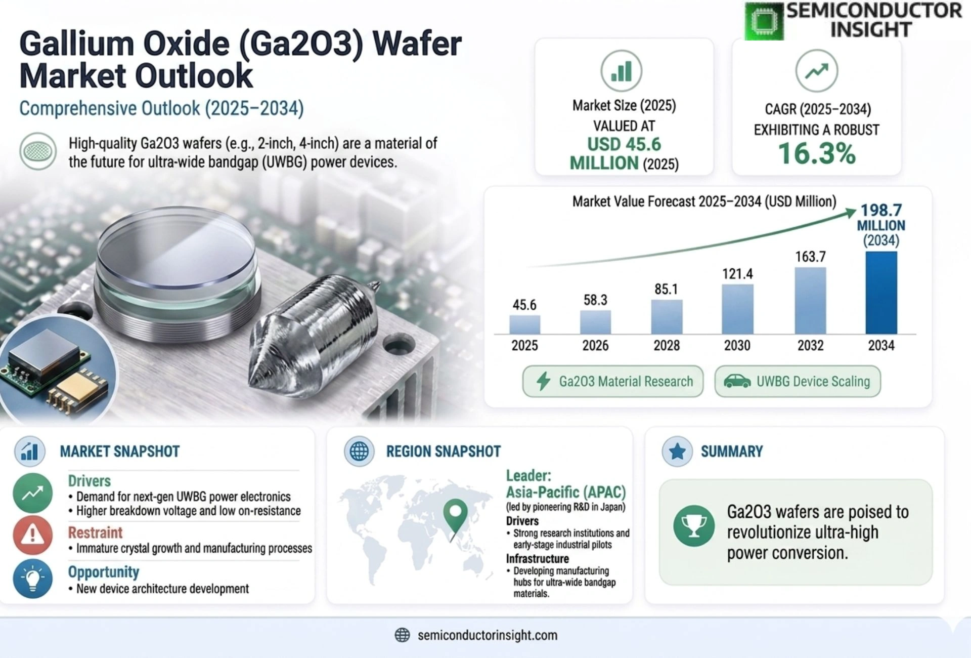
Global Gallium Oxide (Ga2O3) Wafer Market size was valued at USD 45.6 million in 2025. The market is projected to grow from USD 58.3 million in 2026 to USD 198.7 million by 2034, exhibiting a CAGR of 16.3% during the forecast period.
Gallium oxide (Ga2O3) wafers are advanced semiconductor substrates characterized by their ultra-wide bandgap (~4.8 eV), high breakdown voltage, and exceptional thermal stability. These properties make them ideal for high-power electronic devices, deep ultraviolet (UV) photodetectors, and next-generation radio frequency (RF) applications. Unlike traditional silicon-based wafers, Ga2O3 wafers enable superior efficiency in power conversion systems, particularly in electric vehicles (EVs), renewable energy infrastructure, and aerospace electronics. The material is typically synthesized via melt-growth techniques such as Edge-defined Film-fed Growth (EFG) or Czochralski methods, ensuring high crystalline quality for industrial adoption.
While the market remains in its nascent stage compared to established semiconductor materials like silicon carbide (SiC) and gallium nitride (GaN), strategic investments from governments and private enterprises are accelerating commercialization. For instance, the U.S. Department of Defense’s Microelectronics Commons initiative allocated over USD 11 million in 2023 to advance Ga2O3-based technologies for defense applications. Furthermore, Japan’s New Energy and Industrial Technology Development Organization (NEDO) has prioritized Ga2O3 research under its Ultra-Wide Bandgap Semiconductor program, targeting a 50% reduction in power loss for high-voltage devices by 2030.
The rapid expansion of the electric vehicle market, which surpassed 14 million units globally in 2023 (International Energy Agency), is a key driver for Ga2O3-based power modules due to their ability to operate at higher temperatures with minimal cooling requirements.
MARKET DRIVERS
Rising Demand for High-Efficiency Power Devices
The increasing global shift towards renewable energy systems necessitates components that can handle higher voltages with minimal energy loss. Gallium Oxide (Ga2O3) Wafer Market is growing as these wafers offer superior electron mobility and a wider bandgap compared to traditional silicon, making them ideal for next-generation power electronics. Industries are pivoting towards wide-bandgap (WBG) materials to meet efficiency standards for smart grids and high-voltage transmission, which in turn boosts the demand for specialized Ga2O3 substrates that support these advanced semiconductor architectures.
Adoption in Electric Vehicle Infrastructure
With the rapid expansion of electric vehicle (EV) production and fast-charging station networks, industry needs robust and efficient components. Gallium Oxide (Ga2O3) wafers are currently being evaluated and implemented for on-board chargers and traction inverters due to their ability to reduce system size and thermal management requirements. As automakers aim to extend driving range and reduce reliance on rare earth elements, the unique properties of Ga2O3 wafers are becoming a critical factor in the selection of power semiconductor materials for Gallium Oxide (Ga2O3) Wafer Market.
➤ Advancements in epitaxial growth techniques are driving down costs for Gallium Oxide (Ga2O3) wafers.
Furthermore, government initiatives in regions like North America and Europe are funneling significant funds into wide-bandgap semiconductor research. This financial backing accelerates the commercialization of Ga2O3 technology, ensuring steady growth for manufacturers and suppliers Gallium Oxide (Ga2O3) Wafer Market.
MARKET CHALLENGES
High Initial Manufacturing Costs
Producing Gallium Oxide (Ga2O3) wafers requires specialized equipment and expertise that differs significantly from standard silicon manufacturing. The scarcity of skilled labor and the complexity of the synthesis process result in elevated production costs, which can slow down mass adoption in price-sensitive sectors. While efficiency gains are high, the initial capital expenditure (CapEx) required to establish Ga2O3 fabrication lines remains a substantial hurdle for new entrants aiming to capture market share.
Other Challenges
Material Purity and Defects
Maintaining atomic-level perfection in large Ga2O3 boules is difficult, leading to surface defects that impact yield rates.
Standardization of Testing
There is currently a lack of universal testing standards for Ga2O3 devices compared to well-established silicon and silicon carbide protocols.
MARKET RESTRAINTS
Limited Wafer Diameter Availability
Gallium Oxide (Ga2O3) Wafer Market faces a significant bottleneck regarding the size of available substrates. Currently, production capabilities are largely limited to smaller diameters (usually up to 6 inches), whereas silicon markets thrive on large-diameter (8 to 12 inches) wafers. This limitation restricts the scalability of device manufacturing and influences the yield per wafer, making it difficult for established semiconductor giants to ramp up production quickly enough to meet global demand forecasts.
Current manufacturing methods for bulk Ga2O3 lack the throughput needed to compete with established silicon production facilities, resulting in high per-unit costs and limited scalability. This technological gap remains a primary barrier for integrating Ga2O3 semiconductors into high-volume consumer electronics markets where economies of scale are essential for profitability.
MARKET OPPORTUNITIES
Potential for 6G and RF Applications
As the telecommunications industry gears up for Fifth Generation (5G) and Sixth Generation (6G) wireless communications, the demand for high-frequency, high-power devices is surging. Gallium Oxide (Ga2O3) Wafer Market is positioned to capitalize on this trend due to its inherent material properties that suit millimeter-wave applications. Telecom providers are actively seeking substrates that can reduce signal loss and improve power density, creating a lucrative niche for Ga2O3 wafers in next-generation base stations and infrastructure.
Integration with Existing Silicon Foundries
There is a substantial opportunity to integrate Ga2O3 wafer processes into current silicon fabrication environments. As foundries begin to offer dedicated Ga2O3 pilot lines, the barrier to entry for device manufacturers will decrease, fostering innovation and speeding up the commercial deployment of power electronics. This hybrid approach allows established players to leverage their current infrastructure while entering Gallium Oxide (Ga2O3) Wafer Market, minimizing disruption and maximizing efficiency.
Trends
Technological Advancements in Ultra-Wide Bandgap Substrates
Recent developments in Gallium oxide (Ga2O3) wafers are reshaping the landscape of high-power electronics through the introduction of an ultra-wide bandgap of 4.8 eV. This material structure offers critical advantages over traditional silicon, including high breakdown voltage and exceptional thermal stability. The fabrication of these substrates involves sophisticated synthesis techniques such as Edge-defined Film-fed Growth, ensuring high crystalline quality for industrial demands. These properties make Ga2O3 wafers ideal for next-generation radio frequency applications and deep ultraviolet photodetectors, facilitating superior efficiency in power conversion systems. As industries move away from legacy materials, the adoption of Ga2O3 is enabling significant performance improvements in electric vehicles and renewable energy infrastructure.
Other Trends
Strategic Commercialization and Government Support
Despite being in a nascent stage compared to silicon carbide and gallium nitride, the market is gaining momentum through substantial strategic investments. Governments are actively facilitating the commercialization of this technology to secure semiconductor supply chains. For instance, the U.S. Department of Defense has allocated significant funding through initiatives like Microelectronics Commons to advance Ga2O3 capabilities specifically for defense applications. Similar progress is evident in Japan, where the New Energy and Industrial Technology Development Organization has integrated Ga2O3 research into national programs aimed at achieving major reductions in power loss. These policy-driven efforts are essential for addressing current material challenges and accelerating the transition from lab environments to mass production.
Market Demand from Power Electronics and EV Sectors
The commercial viability of Gallium Oxide (Ga2O3) Wafer Market technologies is increasingly driven by the exponential growth in the electric vehicle sector, which surpassed 14 million units globally. These wafers are critical for power modules that require operation at higher temperatures with minimal cooling requirements, directly addressing efficiency bottlenecks in EV manufacturing. Furthermore, the ongoing rollout of 5G infrastructure relies on RF components that demand high efficiency at high voltages. The unique material physics of Ga2O3 support this technological shift, enabling lower power losses and better thermal management. As both the automotive and telecommunications industries set ambitious efficiency targets, the reliance on these advanced wafers is set to increase robustly.
COMPETITIVE LANDSCAPE
Key Industry Players
Market Analysis and Investment Drivers
Global Gallium Oxide (Ga2O3) Wafer Market was valued at USD 45.6 million in 2025 and is anticipated to grow to USD 198.7 million by 2034, reflecting a robust CAGR of 16.3% during the forecast period. These ultra-wide bandgap substrates, characterized by their high breakdown voltage and exceptional thermal stability, are increasingly relied upon for high-power electronics in deep ultraviolet photodetectors and electric vehicles. Unlike traditional silicon, Ga2O3 enables superior efficiency in power conversion systems, typically synthesized via melt-growth techniques such as Edge-defined Film-fed Growth (EFG) to ensure high crystalline quality for industrial adoption.
Strategic investments are fueling this expansion significantly, with the U.S. Department of Defense’s Microelectronics Commons initiative allocating over USD 11 million in 2023 to advance Ga2O3-based technologies for defense applications. Simultaneously, Japan’s NEDO prioritized Ga2O3 research under its Ultra-Wide Bandgap Semiconductor program, targeting a 50% reduction in power loss for high-voltage devices by 2030. The rapid growth of the global EV market, which surpassed 14 million units in 2023, creates substantial demand for Ga2O3-based power modules capable of operating at elevated temperatures with reduced cooling requirements, alongside their deployment in next-generation radio frequency (RF) infrastructure.
List of Key Semiconductor Companies
- Sumitomo Electric Industries
- Sumitomo Electric Industries
- IQE
- IQE
- Ube Industries
- Northrop Grumman
- Monolith Semiconductor
- Norstel
- Transphorm
- Transphorm
- Gaintel
- Nanjing University
Segment Analysis:
| Segment Category | Sub-Segments | Key Insights |
| By Type |
|
Bulk Crystal Substrates form the foundation of the market, providing the necessary mechanical structure for high-power density devices, while thin film epitaxial layers offer versatility in tailoring electronic properties for specific circuit applications. |
| By Application |
|
Power Electronics sector drives innovation due to the material’s exceptional thermal stability and high breakdown voltage, allowing significant improvements in efficiency for electric vehicle power modules and renewable energy conversion systems. |
| By End User |
|
Automotive Industry is transitioning to improve thermal management in electric vehicle power trains, whereas the aerospace and defense sectors prioritize reliability and performance in extreme thermal environments where traditional materials often fail. |
| By Synthesis Method |
|
Melt Growth Techniques are critical to the commercialization roadmap as they provide a scalable pathway to produce the large-diameter wafers required for mass-market semiconductor production, ensuring high crystalline quality without compromising material properties. |
| By Voltage Class |
|
High Voltage Requirements leverage the intrinsic breakdown strength of Gallium Oxide, allowing for superior performance in power conversion applications that minimize energy loss and reduce the need for complex cooling systems compared to conventional semiconductors. |
Regional Analysis
The expansion of Gallium Oxide (Ga2O3) Wafer Market is heavily propelled by the relentless industrial pursuit of energy efficiency and superior thermal management. Manufacturers are increasingly shifting away from traditional silicon-based components toward wide-bandgap materials, recognizing the superior breakdown voltage and higher thermal conductivity capabilities of gallium oxide. This critical transition is driven by the essential need to reduce energy losses in power conversion systems, particularly in electric vehicles, renewable energy generation, and high-frequency computing. The growing technical awareness among stakeholders regarding the long-term operational cost savings associated with gallium oxide technology acts as a significant, sustained demand enhancer for Gallium Oxide (Ga2O3) Wafer Market. Additionally, the shrinking form factor of integrated circuits necessitates materials that can perform reliably under extreme conditions, further establishing the market’s role in enabling next-generation electronic miniaturization and smart grid capabilities.
Supply chain dynamics withGallium Oxide (Ga2O3) Wafer Market are undergoing a significant evolution from a fragmented structure into a more integrated and highly resilient industrial ecosystem. As the complexity of $\beta$-Ga2O3 production increases, leading wafer manufacturers are focusing on vertical consolidation to closely monitor quality control and material consistency from raw gallium extraction to final wafer delivery. This strategic shift aims to mitigate the substantial risks associated with global logistics disruptions that have historically impacted semiconductor availability and pricing. Strategic partnerships between specialty material mining operations and advanced wafer producers are becoming increasingly prevalent, ensuring a stable, long-term supply of raw materials necessary for large-scale fabrication. Furthermore, the strong emphasis on the localization of supply chains is gaining significant traction in major manufacturing hubs, effectively reducing dependency on limited, international transit routes and securing the market’s future scalability.
Regulatory frameworks designed to combat climate change and promote sustainable industrial practices are indirectly, yet powerfully, fueling the organic growth of Gallium Oxide (Ga2O3) Wafer Market. By setting stringent energy efficiency standards for power grids, industrial motors, and green energy systems, governments worldwide are incentivizing the adoption of components that offer lower power losses and superior reliability. Gallium Oxide (Ga2O3) Wafer Market benefits immensely from these policies, as the material’s inherent properties align perfectly with critical environmental mandates for reducing carbon footprints. For instance, the global push for smart grid integration and renewable energy expansion creates a natural, high-demand ecosystem for robust, high-voltage switching devices that can operate without degradation in harsh weather conditions. Compliance with international standards regarding electronic waste and material toxicity also encourages the adoption of safer, more durable materials like gallium oxide, which contributes positively to the market’s long-term societal value and commercial trajectory.
Business strategies withGallium Oxide (Ga2O3) Wafer Market are increasingly characterized by a focused, deep commitment to research and development to overcome inherent technical limitations. Companies are investing significantly in scaling up their 4-inch and larger wafer fabrication lines to meet the surging commercial demand that currently outstrips available global production capacities. Market players are also exploring new applications in high-frequency, high-power microwave devices and space-grade electronics, which could unlock entirely new, high-value revenue streams beyond traditional consumer power electronics. Differentiation is a key competitive advantage, with leading manufacturers seeking to patent unique, proprietary fabrication processes that offer superior crystal quality and lower defect densities, making their wafers essential for elite semiconductor designers. Strategic alliances between specialized materials suppliers and major end-users are becoming increasingly common to validate Ga2O3 technology in real-world applications, thereby accelerating global market penetration and establishing long-term, stable contractual relationships for future expansion.
North America
North America represents a critical and highly specialized frontier for Gallium Oxide (Ga2O3) Wafer Market, driven primarily by rigorous investments in defense technologies, telecommunications, and cutting-edge industrial automation. The region’s advanced infrastructure and the strategic presence of leading automotive and aerospace manufacturers are aggressively pushing the demand for high-frequency, high-efficiency switching devices capable of operating in extreme environments. Regulatory bodies in the United States are actively funding domestic semiconductor alternatives to reduce reliance on foreign supply chains, creating a uniquely favorable investment environment for local gallium oxide wafer producers to establish pilot lines and full-scale manufacturing facilities. The market dynamics here are heavily skewed toward high-value, mission-critical applications rather than mass-market commodity devices, allowing for premium pricing models that sustain profitability for specialized research divisions. However, the market faces distinct challenges related to the historically high cost of essential raw materials and the acute need for a highly specialized workforce, requiring continuous, targeted educational initiatives to bridge the critical skills gap in advanced materials engineering and processing technologies.
Europe
Europe is witnessing a steady, methodical rise Gallium Oxide (Ga2O3) Wafer Market, largely fueled by the region’s strong, unwavering commitment to energy efficiency, green technology, and electromobility. Leading European automotive giants are progressively integrating Ga2O3 based power modules into their next-generation electric drivetrains to enhance vehicle range and significantly reduce complex thermal management requirements. The industrial sector’s profound focus on Industry 4.0 smart manufacturing creates a technical working environment that inherently favors the deployment of wide-bandgap materials in automated control systems and high-speed motor drives. Furthermore, stringent EU regulations regarding carbon emissions and energy conservation are compelling energy distribution companies to upgrade legacy transmission and distribution systems with more efficient, high-reliability hardware, indirectly and heavily boosting the market for gallium oxide wafers. Strategic collaborations between European research consortia and established semiconductor companies are fostering deep, continuous innovation in advanced material processing, ensuring that the region remains competitive and innovative in the global race for next-generation power electronics solutions.
Asia-Pacific (Rest of Region)
Within Asia-Pacific, specifically regarding the broader manufacturing landscape distinct from the leading regional hub, Gallium Oxide (Ga2O3) Wafer Market is characterized by hyper-competitive pricing models and the rapid, scalable capacity expansion of production capabilities. The region’s unparalleled ability to aggregate vast pools of engineering human capital and technical expertise enables wafer manufacturers to achieve economies of scale that are unmatched globally across the semiconductor supply chain. Manufacturing hubs in countries like Taiwan, Singapore, and Southeast Asian nations are positioning themselves as indispensable, key distribution nodes for global wafer demand, leveraging advanced lithography and etching techniques to produce ultra-high-purity substrates with high yields. This region is also seeing significant, growing activity in the recycling and refinement of gallium metals, providing critical support for the circular economy within the material science market. The aggressive, competitive pursuit of market share Gallium Oxide (Ga2O3) Wafer Market has led to a flood of new entrants, effectively driving down pricing barriers and stimulating widespread adoption across various sophisticated consumer, commercial, and industrial electronics sectors.
South America
South America is an emerging, highly promising region with growing potential Gallium Oxide (Ga2O3) Wafer Market, primarily driven by substantial, strategic investments in solar energy infrastructure and smart, precision agricultural technologies. The region’s abundant natural renewable resources necessitate highly efficient, robust power management systems, creating a sustained demand for the advanced semiconductor capabilities offered by Ga2O3 technology. While the local wafer fabrication industry is currently in its early developmental stages, the region effectively serves as a valuable, growing market for imported high-performance electronic components, fostering a robust, upward demand for high-reliability, industrial-grade devices. Forward-looking trade policies in South America are beginning to favor domestic technology manufacturing and localization, which could eventually lead to the establishment of localized wafer production capabilities tailored specifically to the region’s unique, intense grid modernization and rural electrification needs. As the regional economy modernizes and digitalizes, Gallium Oxide (Ga2O3) Wafer Market is poised for substantial, gradual, yet consistent expansion in this developing part of the world.
Middle East & Africa
The Middle East and Africa are progressively recognizing the vital, transformative value of Gallium Oxide (Ga2O3) Wafer Market for critical applications in water desalination, heavy industrial manufacturing, and modern data center operations. The arid climate and energy-intensive nature of essential water processing plants make energy-efficient, high-performance power electronics a mandatory investment rather than an optional upgrade for national development. Governments in the region are channeling vital national funds toward modernizing aging electrical grids and enhancing industrial capabilities, activities that inherently require advanced, state-of-the-art semiconductor materials to ensure system longevity. Gallium Oxide (Ga2O3) Wafer Market finds a critical niche here in providing durable, robust components that can withstand harsh environmental conditions such as intense, persistent heat and corrosive salinity exposure. Although the market penetration remains lower compared to established Asian or North American zones, the region represents a significant, long-term opportunity due to its massive, ambitious energy infrastructure modernization plans and growing, diverse appetite for automation and digitalization technologies.
Report Scope
This market research report provides a comprehensive analysis of the Gallium Oxide (Ga?O?) Wafer Market , covering the forecast period 2026–2034. It offers detailed insights into market dynamics, technological advancements, competitive landscape, and key trends shaping the industry.
Key focus areas of the report include:
- Market Overview: The report begins with an overview outlining its current market scenario, key growth indicators, and industry transformation drivers. It discusses macroeconomic factors, demand–supply balance, regulatory landscape, and the strategic role of semiconductors in powering advancements across industries such as automotive, telecommunications, consumer electronics, and industrial automation.
- Market Size & Forecast: Historical data and future projections for revenue, unit shipments, and market value across major regions and segments.
- Segmentation Analysis: Detailed breakdown by product type, technology, application, and end-user industry to identify high-growth segments and investment opportunities.
- Regional Insights: Insights into market performance across North America, Europe, Asia-Pacific, Latin America, and the Middle East & Africa, including country-level analysis where relevant.
- Competitive Landscape: Profiles of leading market participants, including their product offerings, R&D focus, manufacturing capacity, pricing strategies, and recent developments such as mergers, acquisitions, and partnerships.
- Technology Trends & Innovation: Assessment of emerging technologies, integration of AI/IoT, semiconductor design trends, fabrication techniques, and evolving industry standards.
- Market Drivers & Restraints: Evaluation of factors driving market growth along with challenges, supply chain constraints, regulatory issues, and market-entry barriers.
- Stakeholder Insights: Insights for component suppliers, OEMs, system integrators, investors, and policymakers regarding the evolving ecosystem and strategic opportunities.
Primary and secondary research methods are employed, including interviews with industry experts, data from verified sources, and real-time market intelligence to ensure the accuracy and reliability of the insights presented.
FREQUENTLY ASKED QUESTIONS:
What is the current market size of Gallium Oxide (Ga?O?) Wafer Market?
-> Gallium Oxide (Ga2O3) Wafer Market was valued at USD 45.6 million in 2025 and is expected to reach USD 198.7 million by 2034, exhibiting a CAGR of 16.3% during the forecast period.
Which key companies operate in Gallium Oxide (Ga?O?) Wafer Market?
-> Key players include U.S. Department of Defense, Japan’s NEDO, and private enterprises.
What are the key growth drivers?
-> Key growth drivers include expansion of the electric vehicle market, 5G infrastructure, and renewable energy infrastructure.
Which region dominates the market?
-> The market is driven by global strategic investments with a focus on defense and high-voltage applications.
What are the emerging trends?
-> Emerging trends include deep ultraviolet (UV) photodetectors, high-power electronic devices, and next-generation RF applications.

Get Sample Report PDF for Exclusive Insights
Report Sample Includes
- Table of Contents
- List of Tables & Figures
- Charts, Research Methodology, and more...
 Download Sample Report PDF