Key Statistics
Key Takeaways
- Market trajectory: global GaN epitaxial wafer revenue stood at USD 753.43 million in 2025 and is projected to reach USD 3,971.96 million by 2034, representing a 20.3% CAGR during 2026–2034 as radio-frequency and power-conversion device makers specify more engineered semiconductor layers.
- Substrate mix: GaN-On-SiC is the largest type at an estimated ~40% of 2025 revenue; GaN-On-Si follows near ~30% as its manufacturing economics improve on larger diameter silicon production lines, while native GaN retains specialized high-voltage roles.
- Application structure: Microwave RF holds the largest modeled application share near ~41%, with Power Electronics at ~20%; higher-frequency radio amplifiers require consistent epitaxial heterostructures, while power conversion increasingly rewards low-defect, large-area material.
- Wafer diameter: 6-inch epiwafers lead at an estimated ~37% of value, followed by 8-inch material near ~26%; smaller formats remain important in specialist optical and defense programs, and 12-inch work is principally a development opportunity.
- Regional leadership: Asia-Pacific commands an estimated ~49% share in 2025, supported by Japan, China and Taiwan fabrication ecosystems, while North America represents ~23% and Europe ~19% of the modeled revenue base.
- Growth engines: the main demand catalysts are 5G and defense RF front ends, 650V power architectures, higher wafer throughput, improved epitaxial quality, and longer-term 300mm process development rather than a single consumer product cycle.
- Competition: merchant epitaxy suppliers compete on defect control, reproducibility, device qualification and substrate partnerships; equipment manufacturers and semiconductor device brands influence procurement but should not be counted automatically as merchant epiwafer vendors.
- Coverage: the study evaluates 2025–2034 revenue through Type, Application, Wafer Size and five regions, distinguishing merchant epiwafer shipments from bare substrates, packaged chips, completed RF modules and deposition tools.
Gallium Nitride (GaN) Epiwafers Market Overview
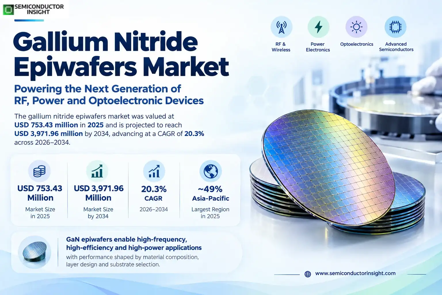
Gallium nitride epiwafers market was valued at USD 753.43 million in 2025 and is projected to reach USD 3,971.96 million by 2034, advancing at a CAGR of 20.3% across 2026–2034. Asia-Pacific represented the largest regional market in 2025, at an estimated ~49%, as compound-semiconductor material producers and downstream fabs increasingly coordinate wafer qualification.
Gallium nitride epitaxial wafers are semiconductor substrates carrying carefully grown GaN, AlGaN and associated buffer layers, rather than merely polished bulk crystal. Their electrical behavior depends on the thickness and composition of multiple films, interface charge, crystalline defects and strain management. These characteristics determine the performance of radio-frequency high-electron-mobility transistors, efficient switching devices and selected optoelectronic emitters before the fabrication of a finished semiconductor chip begins.
The revenue boundary covers commercially supplied GaN epitaxial structures on silicon carbide, silicon, sapphire, native GaN and qualifying alternative substrates. Custom development lots and pilot-production wafers are included where they represent paid material supply. Bare substrates, completed RF power amplifiers, packaged switching devices, LEDs, chargers and MOCVD equipment fall outside the market, although their investment cycles strongly influence demand for epitaxial layers.
Substrate selection divides the economics of this industry. Silicon carbide offers thermal conductivity and radio-frequency performance attractive for demanding high-power amplifiers, whereas silicon permits greater diameter scaling and compatibility with established fabrication infrastructure. Sapphire is associated with optoelectronic manufacturing, while native GaN supports specialist structures requiring lower lattice mismatch. Consequently, one broad material label encompasses several production processes and qualification paths rather than a uniform commodity wafer.
The estimated 2026 market value of USD 906.27 million reflects expansion from established RF deployments into power switching and selected display applications. Suppliers are simultaneously addressing 150mm and 200mm manufacturing programs, while 300mm work remains a technology-development activity with uncertain mass-market conversion timing. Device manufacturers evaluate cost per functioning die, not simply wafer diameter, so an enlarged format must achieve acceptable bow, thickness uniformity and process yield before it becomes commercially superior.
The leading application remains microwave RF because radar, satellite communication and mobile infrastructure require controlled high-frequency gain and thermal behavior. Power electronics provides a different growth profile: a supplier can qualify 650V GaN-on-Si epitaxy for charging and power supplies, yet that material faces stringent dynamic on-resistance, breakdown and lifetime requirements. These separate customer tests mean manufacturing capacity cannot be transferred between applications without process adaptation.
Supply agreements increasingly connect specialist epiwafer producers with foundries, integrated device manufacturers and equipment vendors. Qualification typically begins with small wafer lots, proceeds through electrical and reliability tests, and then expands toward repeated production campaigns. A customer may maintain more than one epitaxy source to protect supply continuity, but switching vendors can require extensive device recharacterization because buffer design and trap behavior affect circuit performance.
Diameter affects gross geometric area before any allowance for edge exclusion or device yield. Nominal 2-inch, 4-inch, 6-inch, 8-inch and 12-inch circles measure 50.8mm, 101.6mm, 152.4mm, 203.2mm and 304.8mm across, corresponding to areas near 20.3, 81.1, 182.4, 324.3 and 729.7 square centimeters. Relative to the smallest format, the idealized area multiples are 1.0, 4.0, 9.0, 16.0 and 36.0; real production economics depend on usable die and defect distribution.
Segment Analysis: By Type
By type, the market comprises GaN-on-Sapphire, GaN-On-Si, GaN-On-SiC, GaN-on-GaN and Others. GaN-On-SiC leads with an estimated ~40% of 2025 value because demanding microwave RF amplifiers favor its thermal and electrical characteristics; GaN-On-Si follows at ~30% and is projected to grow faster as 200mm process qualification spreads. Native GaN and sapphire materials serve different specialist product needs.
| Substrate type | Device and epitaxy characteristics | Commercial positioning |
|---|---|---|
| GaN-On-SiC | Semi-insulating SiC enables AlGaN/GaN high-electron-mobility structures with high power density and strong thermal transport. Epitaxial thickness, buffer design and wafer resistivity are tuned for demanding RF transistor designs in radar, base stations and space communication, with specialized 100mm and 150mm production pathways. | Largest type at ~40% of 2025 revenue; modeled growth near ~19.4% as defense and wireless demand supports high-value wafers. Qualification depends on RF dispersion, thermal performance and defect consistency, and SCIOCS and IQE illustrate supplier capabilities for this demanding category. |
| GaN-On-Si | Silicon substrates permit relatively low-cost scaling into 150mm, 200mm and experimental 300mm processing. Managing thermal expansion mismatch requires engineered buffer stacks, while power devices need controlled leakage, bow and dynamic resistance across large wafer areas before they can enter high-throughput CMOS-compatible lines. | An estimated ~30% of current value, with modeled ~23.5% growth supported by power electronics and wafer-area economics. Qualification complexity remains high because a larger silicon wafer does not automatically produce lower cost per functional die or satisfy automotive lifetime specifications. |
| GaN-on-Sapphire | Sapphire provides an established growth platform for nitride optoelectronics and selected display structures. Film composition and dislocation management are tailored to light emission rather than the highest RF power densities, and customers prioritize emission uniformity, wafer-level defect mapping and downstream lithographic compatibility. | An estimated ~16% share with modeled ~14.5% expansion. The mature LED manufacturing ecosystem supplies a production foundation, while advanced microLED structures create incremental development opportunities that are more sensitive to pixel yield and transfer integration than conventional illumination demand. |
| GaN-on-GaN | Native GaN minimizes crystal-lattice mismatch for specialist vertical and high-voltage devices, offering material properties attractive for designs where substrate defects or interface limitations dominate. Bulk GaN availability, crystal-growth costs and limited large-diameter supply constrain the addressable customer base relative to silicon routes. | An estimated ~10% share, with modeled ~22.0% growth from specialist power and RF research. Customers pay for material performance and reliability potential rather than sheer area throughput, and the segment is less exposed to immediate 200mm commodity-style price competition. |
| Others | This residual category covers qualifying alternative engineered substrate stacks and less common GaN epitaxial configurations. Their manufacturing flows differ from standard SiC, Si, sapphire and native GaN, and suppliers must demonstrate device-level value before specialized approaches are accepted into established semiconductor process sequences. | Approximately ~4% of modeled 2025 revenue with ~16.0% growth. Small engineering programs can achieve high prices per wafer but have limited repeat-volume visibility, so commercial significance depends on the transition from experimental material delivery to stable customer qualification. |
GaN-On-SiC: performance-led RF material
The GaN-On-SiC route combines semi-insulating substrates with epitaxial channels engineered for low trapping and stable power output. At ~40% of 2025 value, it benefits from the high selling price of performance-qualified RF material, but cost and available substrate diameter remain constraints. Qualification cycles for radar and aerospace use can be lengthy because reliability must be demonstrated across temperature, frequency and bias conditions.
GaN-On-Si: expanding the manufacturing envelope
Silicon-based GaN epitaxy carries an estimated ~30% revenue share and the strongest near-term wafer scaling opportunity. Its ~23.5% modeled growth depends on controlling thermal stress and thickness uniformity across 200mm lines while preserving the breakdown performance required by 650V devices. Suppliers that coordinate buffer-stack engineering with foundry process modules can reduce costly qualification iterations.
Sapphire and native GaN: distinct specialist economics
Sapphire supports established optical manufacturing, while GaN-on-GaN addresses selected high-voltage and vertical-device architectures. Their modeled shares of ~16% and ~10% reflect different customer requirements rather than direct interchangeability. A manufacturer of microLED emitters evaluates emission uniformity and wafer yield; a vertical-power developer instead focuses on crystal defects, current conduction and substrate availability.
Segment Analysis: By Application
By application, Microwave RF leads with an estimated ~41% of 2025 revenue, followed by Power Electronics near ~20%. The remaining publisher categories are Photoelectric, Electronic Power, Radio Frequency (RF) Devices and Optoelectronics; the similarly named labels represent separately allocated demand buckets rather than additive overlapping end markets. Device qualification, wafer composition and thermal constraints differ substantially among these applications.
| Application | Demand characteristics |
|---|---|
| Microwave RF | Largest application near ~41% share, with modeled ~19.4% CAGR. GaN HEMT epiwafers serve high-power radio front ends in radar, satellite communication and cellular infrastructure; stable channel charge, buffer leakage and thermal resistance directly affect amplifier efficiency and linearity under demanding duty cycles. |
| Power Electronics | An estimated ~20% of 2025 value and modeled ~25.5% growth, supported by efficient 650V conversion and emerging 100V supply architectures. Silicon-based GaN epitaxy competes on die yield, dynamic on-resistance and the ability to transfer stable device recipes into larger wafer fabrication facilities. |
| Electronic Power | A separately modeled ~12% share, representing power-control and industrial electronic device demand assigned to this publisher category. Growth near ~21.0% reflects demand for switching efficiency, yet procurement remains dependent on device makers qualifying specific material structures for operating voltage, temperature and switching stress. |
| Radio Frequency (RF) Devices | An estimated ~11% share assigned to RF device programs outside the principal Microwave RF bucket, including specialist frequency and module configurations. Modeled ~18.2% growth follows custom qualification programs where low dispersion and reproducible wafer electrical characteristics outweigh lowest-price substrate selection. |
| Photoelectric | A modeled ~9% of current revenue with ~13.8% growth, reflecting optically active device structures and light-sensitive semiconductor applications. Wavelength uniformity, surface morphology and active-layer control are more important here than the thermal power density of RF transistors, leading to different production recipes. |
| Optoelectronics | A modeled ~7% share with ~15.3% expansion, associated with emerging display, microLED and specialized light-emission structures. Customers value consistency across very large numbers of small devices per wafer, making microscopic defects and downstream transfer yield decisive for commercial viability. |
The application labels have overlapping everyday meanings, particularly Microwave RF versus Radio Frequency (RF) Devices and Electronic Power versus Power Electronics. For revenue accounting, the former RF bucket captures major microwave infrastructure programs and the latter captures other RF components; power allocations similarly distinguish the publisher categories by customer program. This separation prevents one epiwafer sale from being counted twice while preserving all published segmentation labels.
High-power RF buyers typically seek GaN-on-SiC because device heating and trapping can undermine amplifier performance, whereas many compact switching customers prioritize 200mm GaN-on-Si economics. Photoelectric and optoelectronic customers may select sapphire or other substrates to achieve optical uniformity. These choices create separate qualification pipelines even when the same supplier operates multiple epitaxy reactors and shares metrology resources.
Regional Analysis
Asia-Pacific is the largest regional GaN epiwafer market, representing an estimated ~49% of 2025 revenue, followed by North America near ~23% and Europe near ~19%. Japan and China provide significant material and downstream semiconductor ecosystems, while Taiwan adds foundry and electronics integration capabilities. North American aerospace and communications programs emphasize qualification; European programs increasingly connect epitaxy to automotive and industrial power conversion.
How do regional manufacturing capabilities shape GaN epiwafer procurement?
Regional differences reflect the location of material growers, device fabs and end-user qualification rather than simple population or electronics consumption. A wafer produced in Japan can be qualified for a United States radar design, while a European foundry may use material developed by a United Kingdom supplier. Therefore regional revenue estimates are best interpreted as a modeled allocation of supplier and customer activity rather than a map of final semiconductor system sales.
Asia-Pacific combines mature compound-semiconductor expertise with the most diverse mix of RF, power and optical customers. North America has a smaller but strategically important defense and high-reliability base, and Europe places more emphasis on industrial power electronics and technology collaboration. Latin America and the Middle East and Africa are mainly downstream electronics and communications markets with limited merchant GaN epitaxial production at scale.
| Region | Position | Growth outlook | Demand profile | What decides supplier selection |
|---|---|---|---|---|
| Asia-Pacific | Largest (~49%) | ~21.8% CAGR | RF, power and optical fabrication | Cross-border qualification, repeatability and substrate access |
| North America | Second (~23%) | ~18.6% CAGR | Defense and communications | Reliability evidence and trusted production continuity |
| Europe | Third (~19%) | ~17.4% CAGR | Industrial and automotive power | 200mm process integration and long-life screening |
| Latin America | Smaller (~5%) | ~21.2% CAGR | Imported electronic components | Distribution and access to qualified material suppliers |
| Middle East & Africa | Emerging (~4%) | ~20.8% CAGR | Telecom and research programs | Project funding, engineering support and technical transfer |
GaN Epiwafer Suppliers and Competitive Landscape
The merchant GaN epiwafer business combines a small group of specialized compound semiconductor growers with integrated device manufacturers that maintain captive epitaxy capacity. Competitive differentiation rests on substrate access, MOVPE process stability, low defect density and the ability to qualify material for an identified RF, power or optical process. A reactor equipment vendor is an enabling supplier, not automatically a competing merchant wafer producer.
IQE markets GaN epitaxial products for RF, power and advanced display applications, while SCIOCS and Sumitomo-related operations provide specialized material and crystal-growth expertise. NTT Advanced Technology describes epitaxial structures across multiple substrates and wafer sizes. Enkris offers GaN-on-Si product pathways, and Soitec participates in engineered substrate technology following its acquisition of EpiGaN. Each company occupies a different position across wafer diameter, material architecture and customer qualification.
Supplier rankings cannot be inferred from overall compound semiconductor company revenue because businesses also sell unrelated photonics, RF chips, substrates and engineering services. For example, a corporate financial statement may disclose broader wireless or power categories without isolating merchant GaN epiwafer shipments. The more relevant competitive indicators are recurring customer approvals, production yields, defect specifications and the proportion of wafers meeting demanding device requirements.
Equipment companies such as AIXTRON and Veeco supply MOCVD reactors that help wafer manufacturers expand capacity, but sales of deposition tools do not enter merchant epiwafer revenue. Similarly, a finished transistor supplier can be a major buyer or captive grower rather than a merchant materials competitor. Treating each value-chain participant as a direct epiwafer vendor would distort both the competitive set and the measured market.
Tier structure
| Tier | Companies | Basis of competition |
|---|---|---|
| Specialist merchant growers | IQE; SCIOCS; NTT Advanced Technology | Process-specific GaN heterostructures, material qualification and repeatable commercial wafer supply |
| Engineered material providers | Soitec; Enkris | Substrate engineering, GaN-on-Si development and differentiated material platforms |
| Captive and adjacent ecosystem | Selected integrated device makers and foundries | Internal epitaxy or wafer fabrication influences purchasing but is not identical to independent merchant sales |
Key companies profiled
- IQE plc
- SCIOCS Company Limited
- NTT Advanced Technology Corporation
- Sumitomo Chemical Co., Ltd.
- Soitec SA
- Enkris Semiconductor, Inc.
GaN Epiwafer Production and Process Economics
GaN epitaxial wafer production requires a tightly controlled sequence of substrate preparation, buffer growth, active-layer deposition, cooling, metrology and electrical screening. Metal-organic chemical vapor deposition is widely used for commercial heterostructures, with process choices determined by the substrate and intended device. Yield loss from bow, thickness nonuniformity, surface defects and trap behavior can outweigh nominal throughput gains from larger reactor capacity.
Growth begins with a substrate whose flatness, orientation and crystalline properties influence every later film. On silicon, engineers use transition and buffer layers to accommodate the mismatch between GaN and the host wafer, while semi-insulating SiC is chosen for high-power RF structures. Wafer preparation must minimize contamination because a defect introduced before epitaxy can propagate through the active layers and compromise finished device yield.
Reactor operation requires repeatable temperature distribution, gas flow and precursor delivery. A production tool may support 150mm or 200mm wafer formats, yet commercially useful throughput depends on achieving uniform layer thickness and electrical properties across each wafer. Routine mapping of sheet resistance, surface morphology and crystal quality allows growers to identify drift before customers encounter device-level failures, reducing expensive scrap and requalification cycles.
Wafer bow and mechanical strength become increasingly important as diameter expands. A 300mm process has the potential to increase die output per run, but it also places tighter demands on stress engineering, substrate handling and downstream lithography. Customers therefore compare usable die cost after all fabrication stages rather than calculate savings from geometric wafer area alone, especially for high-voltage designs with sensitive buffer leakage.
Commercial contracts commonly distinguish engineering wafers, qualification lots and repeated production supply. A prototype shipment can carry a higher price per wafer because it requires specialized recipes and additional metrology, whereas volume programs prioritize stable yields and long-term availability. The transition from sample approval to production can take many process cycles, making the installed base of qualified customer relationships a meaningful competitive asset.
GaN Epiwafers Market Dynamics, Drivers, Restraints and Opportunities
Demand for epitaxial GaN material grows as device manufacturers seek higher RF output density, faster power switching and improved wafer economics. The forecast is shaped by a combination of communications infrastructure, aerospace electronics, industrial power conversion and semiconductor process scaling. Constraints arise from thermal stress, substrate costs, qualification duration and capital-intensive manufacturing, so the pace of adoption differs materially across applications.
MARKET DRIVERS
Drivers Impact Analysis*
| Market Drivers | Impact Rank | CAGR Contribution (%) | 2026–2028 | 2029–2031 | 2032–2034 |
|---|---|---|---|---|---|
| RF amplifier and defense electronics qualification | High | +8.00% | High | High | Medium |
| Efficient power conversion in 650V platforms | High | +6.00% | High | High | High |
| 150mm and 200mm wafer cost improvements | Medium-High | +4.50% | Medium | High | High |
| High-reliability satellite communications demand | Medium | +3.00% | Medium | Medium | High |
| Advanced display and optical material programs | Low-Medium | +2.00% | Low | Medium | Medium |
| Others (specialty device and research demand) | Low | +1.20% | Low | Low | Medium |
RF front-end performance requirements
High-power radio transmitters and radar modules benefit from epitaxial structures engineered for high electron mobility and stable performance under bias. The modeled +8.00 percentage-point driver reflects the value of specialized RF material, where low dispersion and predictable thermal behavior can command a premium. Growth is nevertheless linked to customer qualification and platform life cycles, not simply the number of new mobile network sites.
Power conversion shifts toward GaN switching
GaN power devices can reduce switching losses and enable smaller magnetic components in suitable conversion designs. The +6.00 percentage-point contribution captures the expanding addressable need for qualified epitaxial material in power supplies, charging and selected industrial systems. Material growers must still satisfy device-specific leakage, dynamic resistance and lifetime tests before a technology win becomes repeat wafer revenue.
Larger wafer processing improves economics
Moving compatible designs toward 150mm and 200mm manufacturing can spread fixed process costs across more potential die, contributing a modeled +4.50 percentage points to growth. This benefit is conditional on high usable yield and reliable handling. A larger nominal diameter without uniform electrical properties can increase scrap, so improvements in metrology and reactor control are as important as equipment capacity.
Satellite and aerospace reliability needs
High-frequency satellite links and defense sensing impose demanding temperature, lifetime and power-output specifications on GaN materials. The modeled +3.00 percentage-point effect reflects specialized programs that may pay for stringent screening and traceability. Program schedules can be uneven, but successful qualification creates durable relationships because switching an epitaxy source may require a costly new round of device tests.
Optical and display structures broaden the customer base
Selected microLED and advanced optical device programs use engineered nitride layers with tight composition and surface requirements. Their modeled +2.00 percentage-point growth contribution remains smaller than RF and power because display manufacturing yield and commercialization timing are uncertain. Material suppliers can benefit from development shipments before full production, provided the revenue relates to actual epiwafer supply rather than downstream display systems.
Specialist engineering programs extend material use
Additional applications in sensors, research prototypes and custom semiconductor platforms create a modeled +1.20 percentage-point contribution. These opportunities may involve small paid lots, unusual substrates and extensive technical support rather than commodity volumes. Their aggregate effect is meaningful over a long forecast window, although no single research announcement should be interpreted as proof of sustained commercial wafer shipments.
MARKET RESTRAINTS
Restraints Impact Analysis*
| Market Restraints | Impact Rank | CAGR Contribution (%) | 2026–2028 | 2029–2031 | 2032–2034 |
|---|---|---|---|---|---|
| Crystal stress and wafer bow yield losses | Medium-High | -2.00% | High | High | Medium |
| Substrate and reactor capital intensity | Medium | -1.20% | High | Medium | Medium |
| Long customer qualification and reliability cycles | Low-Medium | -0.80% | High | Medium | Low |
| Others (price competition and inventory swings) | Low | -0.40% | Medium | Medium | Low |
Stress and defect management constrain usable output
Lattice mismatch and thermal expansion differences can generate wafer bow, cracking and electrically active defects, subtracting an estimated 2.00 percentage points from potential growth. The problem becomes more difficult as silicon wafer diameters increase and buffer stacks become complex. Suppliers must invest in epitaxial recipe optimization and inspection to prevent these defects from appearing as low downstream device yields.
Capital costs limit rapid capacity conversion
Compound semiconductor epitaxy requires expensive deposition equipment, controlled precursors, specialist engineering teams and wafer metrology. The modeled 1.20 percentage-point restraint reflects the risk that utilization remains low during customer qualification, particularly when demand shifts among RF, power and optical recipes. Financing capacity before repeat orders are secured can place pressure on smaller merchant material producers.
Qualification timelines delay commercialization
Device manufacturers cannot generally replace an approved epitaxial supplier without checking electrical behavior, reliability and processing compatibility. This delay is modeled as a 0.80 percentage-point restraint, because an attractive material specification does not guarantee immediate production revenue. Automotive and defense programs are particularly demanding, and changes in buffer structure may force extensive retesting even when wafer dimensions remain unchanged.
Pricing pressure and inventory cycles affect orders
Merchant wafer suppliers face customer efforts to reduce unit prices as production volumes increase, while periodic inventory adjustments can postpone new orders. These combined factors account for a modeled 0.40 percentage-point restraint. High-performance custom products retain differentiation, but standardized power materials are more exposed to price comparisons as more manufacturers qualify similar substrate and process configurations.
MARKET OPPORTUNITIES
200mm foundry partnerships for power devices
Joint qualification with established silicon fabs offers a route to scale GaN-on-Si material into repeatable power-device production. A material producer that demonstrates low bow, stable breakdown and predictable electrical uniformity can secure multi-year supply opportunities. The business case should be evaluated at functioning-die cost and process integration maturity rather than at wafer diameter alone.
300mm epitaxy research as a future option
The 300mm development ecosystem is working on larger GaN-on-Si and engineered-substrate approaches, opening a possible long-term path toward higher output per manufacturing cycle. Its commercial value depends on resolving mechanical handling, stress and process reliability. Suppliers with credible pilot capabilities can gain early customer access, but current research demonstrations should not be booked as established high-volume revenue.
Defense and space supply-chain diversification
Aerospace and satellite customers may value multiple qualified material sources to reduce disruption risk in long-lived platforms. Merchant growers that can document lot history, test results and process stability are positioned to win second-source qualifications. The opportunity is commercially attractive because specialized materials can support differentiated pricing, although approval cycles and customer program schedules remain long.
Cross-application process reuse with separate qualifications
Companies capable of running several GaN substrate routes can share inspection expertise and reactor engineering across RF, power and optical products. This flexibility reduces dependence on a single demand cycle without assuming that the same epiwafer fits every application. New revenue is most credible when a specific customer device process is qualified and repeat orders follow successful engineering lots.
GaN Epiwafer Supply Chain and Commercialization
The GaN epitaxial material value chain begins with substrate crystals, chemical precursors and deposition equipment, then moves through wafer growth, inspection and customer qualification before device fabrication. Control of the epitaxial interface is the principal value-adding step for merchant wafer producers. Downstream chip and system revenue is economically connected to the material but must remain outside the merchant epiwafer sales boundary.
Substrate inputs. Wafer material determines thermal behavior, lattice compatibility and the range of device architectures that can be produced economically. Semi-insulating SiC is valuable for high-performance RF applications, while silicon supports larger-diameter power manufacturing. Sapphire and native GaN serve additional specialist needs. Supply continuity, flatness and defect specifications are essential because poor substrate quality cannot be fully corrected by subsequent epitaxial processing.
Deposition and inspection. MOVPE or MOCVD systems deposit the heterostructures that create the electronic or optical function of the eventual device. Growers monitor film thickness, surface defects, electrical properties and mechanical bow to ensure each wafer is fit for customer processing. Equipment makers enable this manufacturing step, but a reactor shipment is not a sale of merchant epitaxial material.
Customer qualification. Foundries and device companies assess engineering wafers through process integration, electrical measurements and reliability tests before signing volume supply agreements. A successful 650V power sample may still need repeated production lots to establish yield stability, while defense RF products can require additional environmental screening. Qualification documentation and technical support often determine whether a merchant supplier is retained.
Device manufacturing. Approved epiwafers are processed into transistor structures, amplifier dies, power switches or optical emitters at downstream fabrication facilities. The same wafer may contribute to a product sold for far more than its starting material cost, but only the merchant epitaxy sale belongs in this market. Separating stages prevents inflated totals when comparing wafer suppliers with chip manufacturers or system integrators.
Recent Developments in the GaN Epiwafers Market
- 7 May 2026 Announced
AIXTRON said it supplied multiple Planetary G5+C GaN MOCVD systems to Renesas for high-volume manufacturing expansion. The order indicates equipment investment in the GaN power-device supply chain and may support future epitaxial capacity, but reactor revenue is distinct from merchant wafer shipments. The commercial significance lies in the need for reproducible growth processes as customers scale qualified power designs. Source - 28 May 2026 Reported
IQE disclosed its full-year 2025 results and described GaN-related capacity investment, power epitaxy qualification and customer activity in RF and advanced display applications. These disclosures indicate the breadth of customer programs for specialized compound semiconductor materials. Corporate revenue also includes unrelated technologies, so the financial totals should not be interpreted as a direct measure of the GaN epiwafer market. Source - 5 November 2025 Announced
Veeco reported an order for its Propel300 MOCVD system from a GaN-on-Si power semiconductor integrated device manufacturer. The announcement shows active investment in 300mm-compatible epitaxial growth equipment, a potential route to larger wafer economics. It does not establish widespread 300mm commercial wafer sales, since customer device yield and manufacturing qualification must follow equipment installation. Source - 6 October 2025 Launched
Imec introduced a 300mm GaN development program involving equipment and semiconductor industry partners. The work targets low- and high-voltage device processes and examines epitaxial growth, mechanical handling and wafer bow challenges. The program is relevant because scaling beyond established 200mm platforms may eventually lower production costs, provided uniformity and downstream electrical performance can be maintained. Source - 10 April 2025 Agreed
IQE and X-FAB announced a joint development agreement for a 650V GaN power semiconductor platform combining epitaxial materials with foundry processing. The collaboration addresses the gap between attractive wafer properties and a manufacturable device flow. For merchant epitaxy suppliers, successful process qualification could create repeat demand for specialized GaN-on-Si material rather than isolated engineering shipments. Source - 19 September 2023 Collaborated
IQE announced a strategic collaboration with VisIC Technologies to develop 200mm depletion-mode GaN power epitaxial wafers for electric-vehicle inverter applications. The agreement illustrates how automotive power customers can influence material specifications well before high-volume adoption. Commercial conversion depends on subsequent device reliability, system design wins and repeatable production yields rather than the initial development announcement. Source
REPORT SCOPE & SEGMENTATION
| Attribute | Details |
|---|---|
| Study Period | 2022–2034 |
| Base Year | 2025 |
| Estimated Year | 2026 |
| Forecast Period | 2026–2034 |
| Historical Reference | 2022–2024 |
| Market Size 2025 | USD 753.43 million |
| Market Size 2026 | USD 906.27 million |
| Market Size 2034 | USD 3,971.96 million |
| Growth Rate | CAGR of 20.3% from 2026–2034 |
| Market Unit | Revenue in USD million; material formats expressed in inches and millimeters |
| Segmentation | By Type, By Application, By Wafer Size and By Region |
| By Type | GaN-on-Sapphire · GaN-On-Si · GaN-On-SiC · GaN-on-GaN · Others |
| By Application | Photoelectric · Electronic Power · Microwave RF · Power Electronics · Radio Frequency (RF) Devices · Optoelectronics |
| By Wafer Size | 2-inch GaN epiwafers · 4-inch GaN epiwafers · 6-inch GaN epiwafers · 8-inch GaN epiwafers · Other sizes (e.g., 12-inch GaN epiwafers) |
| By Region | Regional analysis includes Type, Application, Wafer Size and country-level commercial context. North AmericaUnited States, Canada and rest of North America EuropeUnited Kingdom, Germany, Belgium, France, Italy and rest of Europe Asia-PacificJapan, China, Taiwan, South Korea, India and rest of Asia-Pacific Latin AmericaBrazil, Mexico and rest of Latin America Middle East & AfricaIsrael, United Arab Emirates, South Africa and other regional markets |
| Key Companies Profiled | IQE plc, SCIOCS Company Limited, NTT Advanced Technology Corporation, Sumitomo Chemical Co., Ltd., Soitec SA, Enkris Semiconductor, Inc. |
| Customization Scope | Report customization may extend country coverage, process-level qualification indicators, wafer-size scenarios, supplier benchmarking and specialized application segmentation according to the buyer’s research priorities. |
Frequently Asked Questions
How large is the global GaN epiwafers market in 2025?
The global market is valued at USD 753.43 million for 2025. This measure concerns commercially supplied epitaxial GaN structures rather than the value of finished RF amplifiers, switching transistors or deposition equipment. Asia-Pacific is the largest modeled region, and material sold for high-performance microwave applications forms a substantial part of the revenue base.
What is the forecast value and growth rate through 2034?
The market is projected to reach USD 3,971.96 million by 2034, implying a 20.3% CAGR over 2026–2034. Growth is supported by a wider set of RF, industrial power and specialist optical programs. The forecast assumes gradual improvements in wafer uniformity and customer qualification rather than an immediate transition of all production to the largest experimental wafer formats.
Which substrate category generates the greatest epiwafer revenue?
GaN-On-SiC is the largest modeled type at ~40% of 2025 revenue because semi-insulating silicon carbide supports demanding high-power radio-frequency structures. GaN-On-Si accounts for ~30% and benefits from larger wafer production routes. Sapphire, native GaN and alternative substrates serve distinct applications whose performance needs differ from the dominant microwave RF designs.
What is the leading application for GaN epitaxial materials?
Microwave RF represents an estimated ~41% of current value, reflecting demand for high-electron-mobility transistor structures in radio infrastructure, aerospace communications and radar. Power Electronics follows near ~20%, with separate allocations for Electronic Power and other RF device categories. Each published application label is assigned a distinct revenue bucket to avoid double-counting one material shipment.
Why are six-inch GaN epiwafers commercially important?
Six-inch material is the largest modeled diameter category near ~37% of 2025 value because it balances established production capability with the needs of multiple RF and power customers. Eight-inch wafers represent ~26%, offering a pathway to improved die economics where processes are qualified. Two-inch and four-inch formats continue to serve specialized products and older fabrication infrastructure.
How does GaN-on-Si differ from GaN-on-SiC?
GaN-on-Si emphasizes manufacturability on relatively large silicon substrates, particularly for efficient power switching. GaN-on-SiC is selected where thermal conductivity and RF power performance justify more expensive material. The choice changes buffer-layer engineering, electrical testing and wafer costs; consequently the two routes cannot be treated as interchangeable production inputs merely because both carry gallium nitride epitaxy.
Which companies supply GaN epitaxial wafers?
Relevant material suppliers include IQE, SCIOCS, NTT Advanced Technology, Sumitomo-related operations, Soitec and Enkris, although their products and commercial focus vary. AIXTRON and Veeco supply deposition equipment rather than merchant epiwafers, and some device makers grow material internally. Competitive comparison therefore requires distinguishing independent wafer shipments from captive semiconductor manufacturing and upstream equipment revenue.
Is 300mm GaN already the main commercial wafer format?
No. Development work on 300mm GaN is advancing, but established production remains concentrated in smaller diameters, including 150mm and 200mm platforms. Mechanical bow, film stress, handling and electrical yield require further engineering for large formats. The potential cost benefit is significant, yet a research wafer or installed reactor is not equivalent to a qualified high-volume commercial supply agreement.
What limits the speed of GaN epiwafer adoption?
Material defects, substrate costs, capital-intensive growth equipment and long device qualification cycles are important restraints. Customers test epitaxial structures for leakage, trapping, breakdown and repeatability before placing sustained orders. Larger wafers can improve throughput but also amplify mechanical and uniformity problems, so a manufacturer must demonstrate functioning-device yield rather than rely solely on geometric wafer-area calculations.
Which region offers the largest current market opportunity?
Asia-Pacific is modeled as the largest region at ~49% of 2025 revenue, with Japan, China and Taiwan supporting specialized materials and semiconductor fabrication. North America contributes about ~23% through high-reliability and communications demand, while Europe accounts for roughly ~19% through power electronics and research partnerships. Smaller regions are more dependent on imported devices and project-based wafer procurement.
Research Sources & Evidence Base

Get Sample Report PDF for Exclusive Insights
Report Sample Includes
- Table of Contents
- List of Tables & Figures
- Charts, Research Methodology, and more...
 Download Sample Report PDF