MARKET INSIGHTS
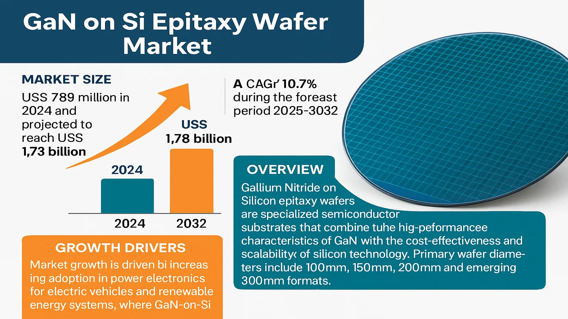
The global GaN on Si Epitaxy Wafer Market size was valued at US$ 789 million in 2024 and is projected to reach US$ 1.78 billion by 2032, at a CAGR of 10.7% during the forecast period 2025-2032.
Gallium Nitride on Silicon epitaxy wafers are specialized semiconductor substrates that combine the high-performance characteristics of GaN with the cost-effectiveness and scalability of silicon technology. These wafers enable the production of high-power, high-frequency electronic devices while maintaining compatibility with existing silicon fabrication infrastructure. The primary wafer diameters include 100mm, 150mm, 200mm and emerging 300mm formats.
The market growth is driven by increasing adoption in power electronics for electric vehicles and renewable energy systems, where GaN-on-Si offers superior efficiency compared to traditional silicon. While the RF semiconductor segment continues to show strong demand, the power device applications are growing faster due to automotive electrification trends. However, yield challenges in larger wafer sizes and thermal management issues remain technical hurdles. Key players like TSMC and GlobalFoundries are investing heavily in 200mm and 300mm GaN-on-Si production capabilities to meet the growing demand from power electronics manufacturers.
MARKET DYNAMICS
MARKET DRIVERS
Demand for Energy-Efficient Power Devices to Propel GaN-on-Si Wafer Adoption
The global push for energy efficiency across industries has significantly accelerated the adoption of Gallium Nitride (GaN) on Silicon (Si) epitaxy wafers. As power consumption becomes a critical concern in consumer electronics, automotive, and industrial applications, GaN-based solutions offer superior performance compared to traditional silicon semiconductors. GaN technology delivers up to 10 times faster switching speeds while reducing power losses by approximately 30%, making it ideal for next-generation power devices. This efficiency advantage has led major semiconductor manufacturers to increasingly integrate GaN-on-Si wafers into their production lines, particularly for applications requiring high-frequency operations and thermal stability.
5G Infrastructure Expansion Creates Strong Demand for GaN RF Components
The ongoing global rollout of 5G networks presents a substantial growth opportunity for GaN-on-Si epitaxy wafers. These wafers are critical for manufacturing high-frequency RF components used in 5G base stations and small cell deployments. With their ability to operate at higher frequencies and power densities than conventional materials, GaN-on-Si solutions enable more efficient signal transmission and reception in the 3.5-6 GHz spectrum bands that are fundamental to 5G networks. The technology’s superior thermal conductivity and breakdown voltage characteristics have positioned it as the material of choice for 5G power amplifiers, with industry forecasts suggesting that nearly 75% of new 5G base stations will incorporate GaN-based RF components by 2025.
MARKET RESTRAINTS
High Production Costs and Yield Challenges Limit Market Penetration
Despite the promising characteristics of GaN-on-Si technology, several significant barriers hinder its widespread adoption. The manufacturing process for GaN epitaxial wafers remains considerably more expensive than traditional silicon wafer production, with current costs estimated to be 3-4 times higher per wafer. This price premium stems from complex deposition techniques required to grow high-quality GaN layers on silicon substrates and the relatively low yields compared to mature silicon processes. The lattice mismatch between GaN and silicon creates defects in the epitaxial layer, requiring sophisticated buffer technologies that add to production complexity and cost. These economic factors currently restrict GaN-on-Si applications primarily to high-value segments where the performance benefits justify the premium pricing.
MARKET CHALLENGES
Thermal Management Issues in High-Power Applications
While GaN devices offer superior thermal properties compared to silicon, managing heat dissipation in high-power applications remains a significant technical challenge. The high power densities achievable with GaN-on-Si devices create localized hotspots that can degrade performance and reliability. Thermal interface materials and packaging solutions that effectively remove heat from GaN devices add complexity and cost to the overall system design. These thermal management challenges become particularly acute in applications such as electric vehicle power systems and data center power supplies, where reliability and continuous operation are critical. Manufacturers are investing heavily in advanced packaging technologies and thermal simulation tools to address these limitations and unlock the full potential of GaN-on-Si technology.
MARKET OPPORTUNITIES
Emerging Applications in Automotive Electrification Present Significant Growth Potential
The rapid electrification of the automotive industry creates substantial opportunities for GaN-on-Si wafer adoption. Electric vehicles require highly efficient power conversion systems for battery management, on-board charging, and traction inverters – all applications where GaN technology offers compelling advantages. As automakers strive to extend vehicle range and reduce charging times, GaN-based power electronics can deliver efficiency improvements of up to 5% compared to silicon solutions. Major automotive suppliers are now qualifying GaN components for next-generation EV platforms, with production volumes expected to scale significantly as the technology achieves automotive-grade reliability certification. This growing automotive demand could accelerate the cost reduction curve for GaN-on-Si wafers through economies of scale.
Advancements in Large-Diameter Wafer Production to Open New Markets
Recent breakthroughs in scaling GaN-on-Si production to larger wafer diameters (200mm and 300mm) present significant market expansion opportunities. The transition from traditional 100mm and 150mm wafers to larger formats could potentially reduce manufacturing costs by 30-40% through improved throughput and better utilization of semiconductor fabrication equipment. Several leading foundries have successfully demonstrated high-quality GaN epitaxy on 200mm silicon substrates, paving the way for volume production in mainstream CMOS fabrication facilities. This compatibility with existing semiconductor manufacturing infrastructure significantly lowers the barrier to entry for new players and enables faster technology adoption across diverse application segments, from consumer fast-charging adapters to industrial motor drives.
GALLIUM NITRIDE (GAN) ON SILICON (SI) EPITAXY WAFER MARKET TRENDS
Increasing Demand for Power Electronics and 5G Infrastructure Fuels Market Growth
The global Gallium Nitride (GaN) on Silicon (Si) epitaxy wafer market is experiencing significant expansion, driven by the escalating demand for high-efficiency power electronics and next-generation 5G infrastructure. GaN-on-Si wafers offer superior performance in power devices, including faster switching speeds and lower energy losses compared to traditional silicon-based solutions. The adoption of GaN technology in electric vehicles, fast-charging systems, and renewable energy applications has grown by an estimated 35% year-over-year in 2023. Furthermore, 5G base stations increasingly incorporate GaN-on-Si RF chips due to their ability to handle high-frequency signals with minimal heat dissipation. This dual application in power and RF sectors positions the market for long-term sustained growth.
Other Trends
Transition to Larger Wafer Sizes for Cost Efficiency
GaN-on-Si wafer manufacturers are progressively shifting from 150mm to 200mm wafers to achieve better economies of scale and reduce per-unit costs. This transition aligns with existing silicon fabrication infrastructure, allowing semiconductor foundries to repurpose mature production lines. The 300mm wafer segment is projected to witness accelerated adoption from 2025 onward as defect densities improve, with several leading foundries already piloting production. This evolution mirrors the historical trajectory of silicon wafer development, where larger diameters consistently delivered cost reductions of 20-30% per generation.
Strategic Collaborations Strengthen Supply Chain Resilience
Heightened geopolitical tensions and pandemic-induced disruptions have prompted vertical integration strategies across the GaN-on-Si ecosystem. Recent alliances between epitaxial wafer suppliers and power semiconductor manufacturers aim to secure reliable substrate sources while optimizing the heteroepitaxy process. The industry has seen over 15 major partnerships announced in 2023 alone, targeting joint development of advanced buffer layer technologies to minimize lattice mismatch challenges. These collaborations not only mitigate supply risks but also accelerate the qualification of automotive-grade GaN devices, which require stringent reliability standards.
COMPETITIVE LANDSCAPE
Key Industry Players
Leading Firms Invest in GaN-on-Si Innovation to Meet Rising Semiconductor Demand
The global Gallium Nitride (GaN) on Silicon (Si) epitaxy wafer market features a mix of established semiconductor manufacturers and specialized GaN technology developers. While the landscape remains highly competitive, TSMC (Taiwan Semiconductor Manufacturing Company) currently dominates with over 30% market share in 2024, owing to its extensive fabrication capabilities and strategic partnerships with power electronics manufacturers.
X-FAB and GlobalFoundries have emerged as strong competitors, particularly in the RF applications segment where GaN-on-Si wafers demonstrate superior performance for 5G infrastructure. Their growth is further propelled by the automotive industry’s shift toward electric vehicles, which require efficient power conversion systems.
Chinese players like San’an Optoelectronics and Enkris Semiconductor are rapidly expanding their market presence through aggressive R&D investments and government-backed semiconductor initiatives. This regional growth aligns with Asia’s position as the largest consumer of GaN-on-Si wafers, accounting for nearly 48% of global demand in 2024.
Meanwhile, U.S.-based Transphorm continues to strengthen its position in power device applications through proprietary GaN-on-Si manufacturing techniques. The company’s recent partnership with a major Japanese automotive supplier highlights the increasing cross-border collaborations in this space.
List of Key GaN-on-Si Epitaxy Wafer Companies Profiled
- TSMC (Taiwan)
- X-FAB Silicon Foundries (Germany)
- Transphorm (U.S.)
- Enkris Semiconductor (China)
- Jvjing Energy (China)
- San’an Optoelectronics (China)
- GlobalFoundries (U.S.)
- Xuzhou GSR Semiconductor (China)
- CSW-Xiamen (China)
- Episil-Precision (Taiwan)
Segment Analysis:
By Type
300 mm Wafer Segment Leads Due to Its Wider Adoption in High-Volume Semiconductor Manufacturing
The market is segmented based on wafer size into:
- 100 mm
- 150 mm
- 200 mm
- 300 mm
By Application
GaN-on-Silicon Power Devices Segment Dominates Owing to Rising Demand for Energy-Efficient Power Electronics
The market is segmented based on application into:
- GaN-on-Silicon Power Devices
- GaN-on-Silicon RF Chip
- GaN-on-Silicon LED Chip
By End User
Consumer Electronics Segment Holds Significant Share Due to Increasing Demand for High-Efficiency Devices
The market is segmented based on end user into:
- Consumer Electronics
- Automotive
- Telecommunications
- Industrial
- Others
By Technology
MOCVD Technology Segment Leads Owing to Its Superior Deposition Capabilities
The market is segmented based on technology into:
- MOCVD (Metal-Organic Chemical Vapor Deposition)
- MBE (Molecular Beam Epitaxy)
- HVPE (Hydride Vapor Phase Epitaxy)
- Others
Regional Analysis: Gallium Nitride (GaN) on Silicon (Si) Epitaxy Wafer Market
Asia-Pacific
The Asia-Pacific region is the undisputed leader in the GaN-on-Si epitaxy wafer market, holding the largest share due to robust semiconductor manufacturing ecosystems in China, Japan, and South Korea. With China’s push for semiconductor self-sufficiency and investments exceeding $100 billion in domestic fabrication, demand for GaN-on-Si wafers is accelerating. Japan leverages its expertise in compound semiconductors, while South Korea’s vertically integrated electronics giants are driving adoption for 5G and power electronics applications. The region accounts for over 50% of global GaN wafer production capacity, though recent supply chain disruptions caused a 2% contraction in 2022.
North America
North America shows strong technological leadership in GaN innovation, particularly in RF and power device applications. The U.S. Department of Defense investments in GaN technologies and growing adoption in data center power systems are key drivers. With semiconductor sales growing 17% year-on-year, the region is seeing increased fab capacity from players like GlobalFoundries and Transphorm. However, higher production costs compared to Asia and dependence on foreign suppliers for raw materials present challenges. The U.S. CHIPS Act is expected to provide crucial support for domestic GaN wafer production.
Europe
Europe maintains a competitive position in GaN-on-Si technology through specialized foundries like X-Fab and strong research institutions. The region benefits from government initiatives supporting wide-bandgap semiconductors, with Germany and France leading in automotive and industrial applications. While wafer production capacity is limited compared to Asia, Europe excels in patented GaN-on-Si processes for high-performance RF applications. The market faces challenges in scaling production to compete with Asian cost structures, though collaboration through programs like the European Chips Act aims to strengthen the supply chain.
South America
The South American market remains nascent for GaN-on-Si wafers, primarily serving niche industrial applications through imports. Brazil shows potential with its electronics manufacturing base, but unstable economic conditions and limited semiconductor infrastructure hinder local production. Most demand comes from academic research institutions and select power electronics manufacturers. While some regional players are exploring partnerships with Asian wafer suppliers, the market is expected to develop slowly without significant government support for semiconductor initiatives.
Middle East & Africa
This region presents minimal GaN-on-Si wafer production but shows strategic interest in semiconductor technology, particularly in Israel’s defense sector and the UAE’s technology diversification efforts. Limited local demand and high infrastructure costs prevent wafer fabrication investments, with most applications relying on imports. However, long-term initiatives like Saudi Arabia’s Vision 2030 include semiconductor development goals that may gradually increase regional engagement with GaN technologies, primarily through research partnerships and pilot production facilities.
Key Regional Competitive Landscape
While TSMC and San’an Optoelectronics dominate Asian production, North American players like Transphorm specialize in power device wafers, and Europe’s X-Fab maintains strengths in automotive-grade solutions. The market remains highly dependent on Asia for volume production, with other regions focusing on specialized high-value applications where they maintain competitive advantages.
Report Scope
This market research report provides a comprehensive analysis of the global Gallium Nitride (GaN) on Silicon (Si) Epitaxy Wafer market, covering the forecast period 2025–2032. It offers detailed insights into market dynamics, technological advancements, competitive landscape, and key trends shaping the industry.
Key focus areas of the report include:
- Market Size & Forecast: Historical data and future projections for revenue, unit shipments, and market value across major regions and segments.
- Segmentation Analysis: Detailed breakdown by wafer size (100 mm, 150 mm, 200 mm, 300 mm), application (power devices, RF chips, LED chips), and end-user industries.
- Regional Outlook: Insights into market performance across North America, Europe, Asia-Pacific, Latin America, and Middle East & Africa, with country-level analysis.
- Competitive Landscape: Profiles of leading market participants including TSMC, X-Fab, Transphorm, and others, covering product portfolios, R&D investments, and strategic developments.
- Technology Trends: Assessment of emerging fabrication techniques, integration with power electronics, and advancements in GaN-on-Si epitaxial growth processes.
- Market Drivers & Restraints: Evaluation of factors such as 5G deployment, electric vehicle adoption, and challenges in defect density reduction.
- Stakeholder Analysis: Strategic insights for semiconductor foundries, device manufacturers, investors, and policymakers.
The analysis combines primary interviews with industry experts and validated secondary data from reliable sources to ensure accuracy and reliability.
FREQUENTLY ASKED QUESTIONS:
What is the current market size of Global GaN-on-Si Epitaxy Wafer Market?
-> GaN on Si Epitaxy Wafer market size was valued at US$ 789 million in 2024 and is projected to reach US$ 1.78 billion by 2032, at a CAGR of 10.7% during the forecast period 2025-2032.
Which key companies operate in Global GaN-on-Si Epitaxy Wafer Market?
-> Key players include TSMC, X-Fab, Transphorm, Enkris Semiconductor, San’an Optoelectronics, and GlobalFoundries, among others.
What are the key growth drivers?
-> Growth is driven by 5G infrastructure deployment, electric vehicle power electronics adoption, and demand for energy-efficient power devices.
Which region dominates the market?
-> Asia-Pacific holds the largest market share (62% in 2024), led by semiconductor manufacturing in China, Taiwan, and Japan.
What are the emerging trends?
-> Emerging trends include 200mm wafer transition, automotive-grade GaN power devices, and hybrid GaN-on-Si/SiC solutions.

Get Sample Report PDF for Exclusive Insights
Report Sample Includes
- Table of Contents
- List of Tables & Figures
- Charts, Research Methodology, and more...
 Download Sample Report PDF