Gallium Nitride (GaN) Epiwafers for Radio Frequency Market Insights
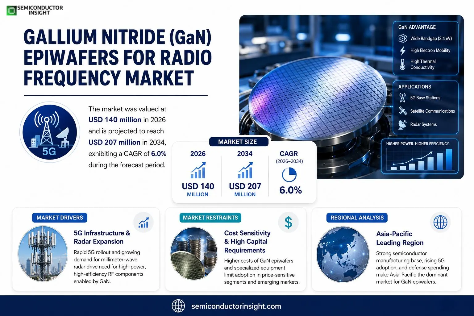
Gallium Nitride (GaN) Epiwafers for Radio Frequency market was valued at USD 140 million in 2026 and is projected to reach USD 207 million by 2034, exhibiting a CAGR of 6.0% during the forecast period.
GaN epiwafers are crystalline substrates produced primarily by metal‑organic chemical vapor deposition (MOCVD). Their wide band‑gap (3.4 eV), high electron mobility and superior thermal conductivity make them ideal for high‑power radio‑frequency components such as power amplifiers, phased‑array antenna modules and radar transceivers. These wafers enable devices that operate at higher voltages and temperatures than silicon equivalents, delivering compact, energy‑efficient solutions for 5G base stations, satellite communications and defense radar systems.The upward trajectory stems from accelerating deployment of 5G infrastructure, expanding use of millimeter‑wave radar in autonomous vehicles, and increasing demand for satellite broadband constellations. Leading suppliersincluding Wolfspeed, NTT AT, Sumitomo’s SCIOCS, Soitec’s EpiGaN and DOWA Electronicsare expanding capacity toward larger diameters (6‑inch and 8‑inch) while refining cost structures to satisfy growing volume needs.
MARKET DRIVERS
Performance Gains Driving Adoption
Engineers are increasingly turning to Gallium Nitride (GaN) Epiwafers for Radio Frequency Market because the material delivers power densities that are two to three times higher than silicon alternatives. The resulting thermal efficiency shortens cooling paths, which in turn lowers bill‑of‑materials for high‑power amplifiers. This technical advantage is reshaping design decisions across mobile backhaul, satellite transceivers and defense radars.
5G Infrastructure and Automotive Radar Expansion
The rollout of 5G networks accelerates demand for RF front‑ends that can handle wider bandwidths without compromising linearity. Simultaneously, automotive manufacturers are equipping next‑generation vehicles with millimeter‑wave radar that requires the high‑frequency performance only GaN can provide. The convergence of these two megatrends translates into a steady influx of orders for high‑quality epiwafers.
➤ Industry analysts estimate that the GaN epiwafer segment now accounts for roughly one‑quarter of all RF‑grade wafer shipments worldwide.
Supply‑chain partners are responding by expanding MOCVD tool capacity and by standardising wafer sizes, which further de‑risks the adoption curve for end‑users. As a result, the competitive landscape is shifting toward firms that can guarantee both performance and volume.
MARKET CHALLENGES
Manufacturing Complexity and Yield Management
Growing GaN epitaxial layers on large diameter substrates demands precise control of temperature gradients and gas flows. Even minor deviations can trigger dislocation networks that erode device reliability. Manufacturers therefore face higher yield variability, which inflates per‑wafer cost and forces customers to maintain larger safety stocks.
Other Challenges
Supply Chain Vulnerabilities
The reliance on high‑purity substrates from a limited pool of vendors creates bottlenecks during periods of rapid demand spikes. Any disruptionwhether geopolitical or logisticalquickly ripples through the RF ecosystem, prompting design teams to evaluate alternate material strategies.
MARKET RESTRAINTS
Cost Sensitivity in Emerging Markets
Price differentials between GaN epiwafers and mature silicon wafers remain pronounced, especially for customers in cost‑driven segments such as IoT gateways. While performance metrics justify the premium, many operators still prioritise total cost of ownership, limiting the pace at which GaN can displace entrenched silicon solutions.In addition, the higher capital outlay required for GaN‑specific device packaging and testing deters smaller players from committing to full‑scale production runs. This financial hurdle narrows the pool of potential adopters and slows market diffusion.Finally, the ecosystem of design‑automation tools for GaN RF circuits is still maturing. Engineers often need to invest additional time in custom simulations, which can increase development schedules and dampen enthusiasm for immediate migration.
MARKET OPPORTUNITIES
Emerging Satellite Constellations
New low‑Earth‑orbit (LEO) constellations demand compact, high‑efficiency transmitters that can operate across Ka‑band and higher frequencies. GaN epiwafers deliver the necessary power handling while maintaining a small footprint, creating a clear opening for suppliers that can guarantee space‑qualified reliability.Beyond communications, defense and aerospace programs are seeking GaN‑based radar modules capable of rapid beam steering and higher peak powers. These applications generate high‑margin contracts and encourage long‑term partnerships with wafer manufacturers.Finally, the convergence of advanced packagingsuch as silicon interposers and fan‑out wafer‑level packagingwith GaN epitaxy is unlocking novel system‑in‑package (SiP) architectures. Companies that integrate these technologies early stand to benefit from differentiated product portfolios and accelerated market share gains.
Gallium Nitride (GaN) Epiwafers for Radio Frequency Market Trends
Accelerating 5G Infrastructure Adoption
The Gallium Nitride (GaN) Epiwafers for Radio Frequency Market recorded revenue of approximately $140 million in 2026 and is forecast to reach $207 million by 2034, reflecting an average annual increase of about 6 percent. The primary catalyst behind this trajectory is the expanding rollout of 5 G networks, which demand high‑power, high‑efficiency RF components. GaN epiwafers deliver superior electron mobility and thermal conductivity compared to silicon, enabling base‑station amplifiers that operate at higher frequencies with lower heat dissipation. Consequently, equipment manufacturers are substituting traditional silicon‑based solutions with GaN‑based modules, driving up wafer orders across the supply chain. The ripple effect is evident in the analog and sensor segments that, while unrelated to RF, share the same substrate technology, thereby amplifying the overall demand for GaN epiwafers.
Other Trends
Supply Chain Consolidation
Over the past two years, the GaN epiwafer ecosystem has witnessed a wave of mergers and strategic alliances. Leading players such as Wolfspeed and NTT AT have acquired niche equipment vendors to secure lithography capacity, while smaller Asian manufacturers are forming consortia to pool R&D resources. This consolidation reduces lead times and stabilizes pricing, which is crucial for telecom operators that require predictable cost structures when scaling 5 G deployments. However, the tightening of supply channels also raises entry barriers for new entrants, potentially limiting innovation from start‑ups that lack scale.
Regional Demand Divergence
Geographically, the market exhibits contrasting trends. North America continues to post double‑digit year‑on‑year growth, propelled by massive carrier investments in mid‑band spectrum and government incentives for advanced communications infrastructure. Europe shows steady expansion, with a focus on automotive radar upgrades for autonomous driving projects. In contrast, the Asia‑Pacific region, which historically accounted for the largest wafer volume, recorded a modest 2 percent decline in 2022, reflecting slower consumer‑electronics demand and tighter macro‑economic conditions. Nonetheless, China’s push for domestic semiconductor self‑sufficiency is expected to revive production volumes within the next three years, especially in the 6‑inch wafer segment that aligns with existing fab lines.
For companies operating in the Gallium Nitride (GaN) Epiwafers for Radio Frequency Market, the converging forces of 5 G rollout, supply‑chain re‑engineering, and regional demand shifts create a nuanced strategic landscape. Executives must balance investments in capacity expansion against the risk of oversupply in markets where growth is decelerating. Simultaneously, leveraging partnerships with chipset designers can unlock higher‑margin applications such as satellite‑communications and high‑frequency radar, where performance advantages of GaN are most pronounced. Agile portfolio management, underpinned by real‑time demand intelligence, will be the decisive factor for sustaining profitability through 2034.
COMPETITIVE LANDSCAPE
Key Industry Players
Gallium Nitride (GaN) Epiwafer Suppliers – Structure and Market Share
The RF GaN epiwafer segment is dominated by a handful of vertically integrated firms that control crystal growth, wafer thinning and finishing. Wolfspeed, leveraging its legacy in SiC and GaN power devices, commands roughly 30 % of shipments, largely because its 200‑mm production line matches the preferred substrate size for 5G base‑station amplifiers. NTT AT, with a strong foothold in Japan’s telecom equipment ecosystem, supplements the market through a joint venture that supplies high‑purity GaN substrates to domestic antenna makers. Both entities benefit from long‑term supply contracts that lock in capacity and provide pricing visibility, a critical advantage in a market where yield improvements translate directly into lower RF insertion loss. Their investment in large‑diameter (200 mm) epitaxy tools also forces smaller competitors to specialize in niche thicknesses or custom doping profiles, reinforcing a tiered structure where scale and reliability drive the top‑tier share.Beyond the core incumbents, a diverse set of niche players addresses specific wafer‑size or performance niches. Soitec’s EpiGaN line targets 150‑mm substrates prized by European radar developers, while DOWA Electronics Materials focuses on ultra‑thin (≤300 µm) wafers for space‑qualified transceivers. IQE and Enkris Semiconductor supply specialty doped layers for high‑frequency mixers, often partnering with design houses to co‑develop thin‑film processes. Chinese manufacturers such as Suzhou Nanowin, Xinguan Technology and Shanxi Yuteng have expanded capacity rapidly, concentrating on cost‑competitive 4‑inch products for regional 5G roll‑outs. CorEnergy and Genettice add value through proprietary passivation and surface‑treatment chemistries that improve power‑added efficiency. This constellation of smaller firms creates a competitive pressure that forces the leaders to continuously refine yield and cost structures, while also presenting acquisition opportunities for larger players seeking to broaden their product portfolio.
List of Key Gallium Nitride (GaN) Epiwafers for Radio Frequency Companies Profiled
- NTT AT
- Wolfspeed
- SCIOCS (Sumitomo)
- EpiGaN (Soitec)
- DOWA Electronics Materials
- IQE
- Enkris Semiconductor Inc
- CorEnergy
- GLC
- Genettice
- Suzhou Nanowin
- Episil-Precision Inc
- Xinguan Technology
- Shanxi Yuteng
Segment Analysis:
| Segment Category | Sub-Segments | Key Insights |
| By Type |
|
4‑inch wafers dominate early‑stage adoption because they fit well with existing legacy equipment and enable lower entry cost for new RF designs.
|
| By Application |
|
5G communications emerge as the leading application due to the need for high‑power, high‑efficiency RF front‑ends.
|
| By End User |
|
Telecom equipment manufacturers lead the end‑user landscape, driven by rapid rollout of advanced network infrastructure.
|
| By Process Technology |
|
MOCVD remains the preferred process because it consistently delivers superior crystalline quality essential for high‑frequency performance.
|
| By Performance Tier |
|
High‑Power tier drives the most attention as it enables compact, efficient transmitters for radar and satellite links.
|
Regional Analysis: Gallium Nitride (GaN) Epiwafers for Radio Frequency Market
North America
The continent’s emphasis on on‑shoring critical wafer steps mitigates exposure to geopolitical shocks. Partnerships between substrate growers and downstream fab operators embed risk‑sharing clauses, ensuring continuity for high‑value RF programs while maintaining flexibility to respond to demand spikes.
Defense radars, satellite transceivers, and 5G base‑stations dominate the order book. Each segment values the power‑density advantage of GaN, prompting OEMs to specify epitaxial quality as a non‑negotiable design parameter in their procurement criteria.
University‑industry consortia accelerate breakthrough processes such as high‑temperature MOCVD. The resulting material insights quickly cascade to commercial fabs, shortening the interval between laboratory discovery and market‑ready wafer shipments.
Export‑control regimes shape the flow of high‑performance GaN wafers. Compliance frameworks compel manufacturers to adopt traceability systems, which paradoxically enhance customer confidence and open avenues for premium service contracts.
Europe
Europe’s market is anchored by a well‑established RF component sector in Germany, France, and the United Kingdom. While the region lags behind North America in substrate capacity, it compensates through aggressive public‑private research initiatives targeting energy‑efficient power amplifiers for 5G and automotive radar. The European Union’s focus on strategic autonomy drives investment in domestic epitaxy lines, encouraging local OEMs to source GaN epiwafers within the bloc. Consequently, supply agreements increasingly include joint‑development clauses that align wafer specifications with emerging EU standards for electromagnetic compatibility, creating a niche of regulated, high‑trust supply chains.
Asia‑Pacific
Asia‑Pacific presents a paradox of rapid demand growth and fragmented production capability. China’s ambitious semiconductor roadmap aims to scale GaN wafer output, yet constraints in high‑purity source material limit immediate expansion. Meanwhile, Japan and South Korea leverage mature MOCVD toolsets to serve niche RF markets, particularly in automotive and industrial communications. The region’s manufacturers prioritize cost efficiency, prompting them to adopt tiered qualification programs that balance performance with volume. This approach fuels a competitive environment where price sensitivity coexists with a willingness to invest in collaborative R&D consortia across borders.
South America
South America remains a nascent arena for GaN epiwafers, with Brazil leading modest pilot projects for satellite uplink stations. The market’s modest size stems from limited local fab infrastructure and a reliance on imported wafers. Nonetheless, governmental incentives aimed at expanding broadband coverage in remote regions have sparked interest in GaN‑based RF front‑ends, which promise higher power efficiency for off‑grid deployments. As telecom operators evaluate network upgrades, the region may witness a gradual shift from experimental deployments to modest volume orders, contingent on the arrival of cost‑effective supply channels.
Middle East & Africa
In the Middle East & Africa, the GaN epiwafer narrative is driven largely by defense modernization programs and the rollout of 5G in affluent Gulf states. Investment funds in the UAE and Saudi Arabia have earmarked capital for establishing localized wafer‑handling facilities, seeking to reduce reliance on external suppliers. African markets, while smaller, are exploring satellite communication solutions to bridge connectivity gaps, where the efficiency of GaN power amplifiers becomes a decisive factor. The combined effect of strategic defense spend and targeted telecom upgrades creates a modest yet growing demand base that could catalyze early‑stage partnerships with wafer producers.
Report Scope
This market research report provides a comprehensive analysis of the Gallium Nitride (GaN) Epiwafers for Radio Frequency Market , covering the forecast period 2026–2034. It offers detailed insights into market dynamics, technological advancements, competitive landscape, and key trends shaping the industry.
Key focus areas of the report include:
- Market Overview: The report begins with an overview outlining its current market scenario, key growth indicators, and industry transformation drivers. It discusses macroeconomic factors, demand–supply balance, regulatory landscape, and the strategic role of semiconductors in powering advancements across industries such as automotive, telecommunications, consumer electronics, and industrial automation.
- Market Size & Forecast: Historical data and future projections for revenue, unit shipments, and market value across major regions and segments.
- Segmentation Analysis: Detailed breakdown by product type, technology, application, and end-user industry to identify high-growth segments and investment opportunities.
- Regional Insights: Insights into market performance across North America, Europe, Asia-Pacific, Latin America, and the Middle East & Africa, including country-level analysis where relevant.
- Competitive Landscape: Profiles of leading market participants, including their product offerings, R&D focus, manufacturing capacity, pricing strategies, and recent developments such as mergers, acquisitions, and partnerships.
- Technology Trends & Innovation: Assessment of emerging technologies, integration of AI/IoT, semiconductor design trends, fabrication techniques, and evolving industry standards.
- Market Drivers & Restraints: Evaluation of factors driving market growth along with challenges, supply chain constraints, regulatory issues, and market-entry barriers.
- Stakeholder Insights: Insights for component suppliers, OEMs, system integrators, investors, and policymakers regarding the evolving ecosystem and strategic opportunities.
Primary and secondary research methods are employed, including interviews with industry experts, data from verified sources, and real-time market intelligence to ensure the accuracy and reliability of the insights presented.
FREQUENTLY ASKED QUESTIONS:
What is the current market size of Gallium Nitride (GaN) Epiwafers for Radio Frequency Market?
-> Gallium Nitride (GaN) Epiwafers for Radio Frequency Market was valued at USD 140 million in 2026 and is expected to reach USD 207 million by 2034, growing at a CAGR of 6.0% during the forecast period.
Which key companies operate in Gallium Nitride (GaN) Epiwafers for Radio Frequency Market?
-> Key players include NTT AT, Wolfspeed, SCIOCS (Sumitomo), EpiGaN (Soitec), DOWA Electronics Materials, IQE, Enkris Semiconductor Inc, CorEnergy, GLC, Genettice, Suzhou Nanowin, Episil-Precision Inc, Xinguan Technology, Shanxi Yuteng, among others.
What are the key growth drivers?
-> Key growth drivers include expanding 5G infrastructure, increasing demand for radar systems, growth of satellite communications, and the need for high‑performance RF components in automotive and defense applications.
Which region dominates the market?
-> Asia‑Pacific is the dominant region for GaN epiwafers, driven by strong semiconductor manufacturing bases and demand from communications and defense sectors, while other regions show steady growth.
What are the emerging trends?
-> Emerging trends include adoption of larger wafer diameters (8‑inch), focus on 5G and radar application development, and integration of GaN technology with advanced packaging solutions.
Get Sample Report PDF for Exclusive Insights
Report Sample Includes
- Table of Contents
- List of Tables & Figures
- Charts, Research Methodology, and more...
 Download Sample Report PDF