Key Statistics
Key Takeaways
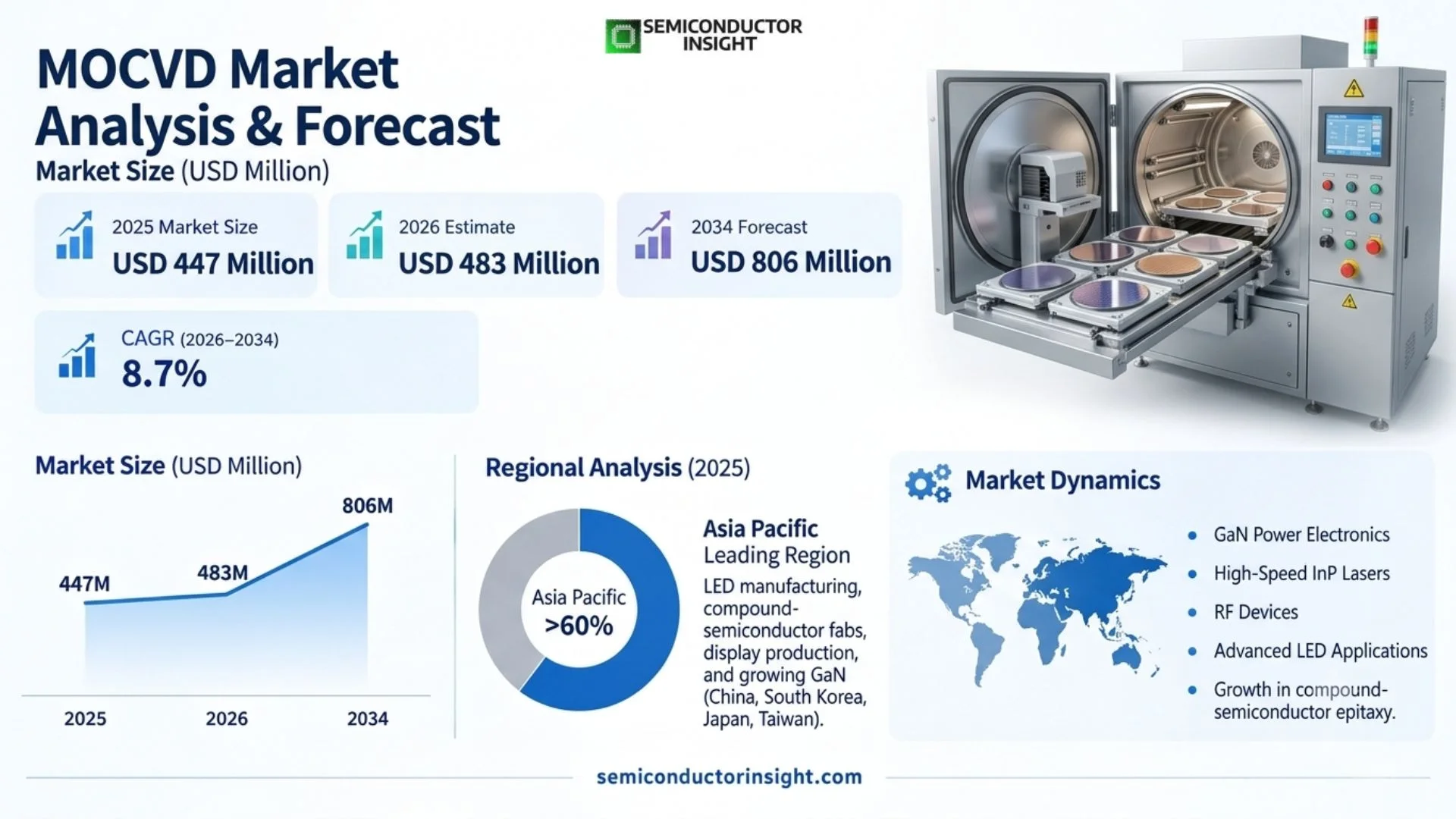
- Market size: The market stands at USD 447 million in 2025 and is projected to reach USD 806 million by 2034, representing a 8.7% CAGR across 2026–2034.
- GaN-based MOCVD is the largest technology segment because LEDs, GaN power devices and RF components require high-quality epitaxial layers with tight control of composition, doping and thickness.
- Asia Pacific leads installed demand through China, South Korea, Japan and Taiwan, where LED, compound-semiconductor and power-device capacity is concentrated.
- 8-inch and 300mm capability is becoming strategically important as power-semiconductor manufacturers seek higher chip output per wafer and compatibility with existing silicon production infrastructure.
- AIXTRON and Veeco remain the most visible global equipment leaders, while Chinese suppliers are increasing their role in domestic GaN and LED manufacturing.
MOCVD Market Overview
MOCVD market is valued at USD 447 million in 2025 and is projected to reach USD 806 million by 2034, expanding at a 8.7% CAGR during 2026–2034. The 2026 market level is USD 483 million. Asia Pacific holds the largest installed base, while demand is broadening beyond conventional LED production toward GaN power electronics, InP lasers for optical interconnects and RF devices. Equipment roadmaps increasingly emphasize larger wafers, in-situ monitoring, lower precursor consumption, process repeatability and higher throughput.
Metal-Organic Chemical Vapor Deposition is an epitaxial growth process used to deposit compound-semiconductor layers from metal-organic precursors and hydride gases. It is central to GaN, GaAs and InP device manufacturing because it enables precise control of composition, thickness, doping and interface quality across multilayer structures. Commercial systems combine reactor chambers, gas delivery, wafer handling, heating, exhaust treatment and process monitoring in configurations optimized for specific materials and wafer diameters.
The equipment base is diverging by application. LED and MicroLED production values uniformity and multi-wafer throughput, GaN power requires low-defect epitaxy on silicon or SiC at larger diameters, and optical communication lasers need exceptional control of InP-based layer thickness and composition. Veeco’s 300mm Propel platform and Lumina InP systems illustrate how MOCVD architectures are being adapted for both high-volume power electronics and data-center optical interconnects.
MOCVD is a capital-intensive market with long qualification cycles because customers must prove film uniformity, defect density, device performance and uptime before moving a reactor into volume production. Revenue therefore includes not only system sales but also service, spare parts, chamber upgrades and installed-base support. The economic value of a tool depends on usable wafer throughput, precursor efficiency, maintenance intervals and the time required to return a chamber to stable production after service.
Segment Analysis: By Type
By type, the market is segmented into GaN-based MOCVD and GaAs/InP-based MOCVD. GaN systems account for the larger installed opportunity because they serve LEDs, GaN power and RF applications, while GaAs/InP systems are critical for laser diodes, photonic integrated circuits and optical communications. The two categories differ materially in precursor chemistry, reactor conditions, wafer sizes and customer process requirements.
| Type | Technical / commercial role | Market position |
|---|---|---|
| GaN-based MOCVD | Epitaxy for LEDs, GaN power, RF and emerging MicroLED production on sapphire, SiC or silicon substrates. | Largest segment, with demand increasingly influenced by power electronics and larger wafer formats. |
| GaAs/InP-based MOCVD | Epitaxy for laser diodes, photonics, datacom/telecom and specialty RF devices. | High-value segment benefiting from AI data-center optical interconnect growth and higher-speed laser requirements. |
Additional Segmentation: By End User
End-user demand is divided among semiconductor foundries, integrated device manufacturers and R&D institutions. IDMs remain the largest users because epitaxial process recipes are closely tied to device architecture and manufacturing yield. Foundries are increasingly important as GaN and compound-semiconductor manufacturing becomes more outsourced, while universities and R&D laboratories support new materials, process development and pilot-line qualification before high-volume adoption.
| End User | Demand characteristics |
|---|---|
| Semiconductor Foundries | Merchant capacity for GaN, RF and photonics customers; purchasing emphasizes platform flexibility and customer-specific process qualification. |
| Integrated Device Manufacturers | Vertical integration of epitaxy and device fabrication; highest value placed on uptime, throughput and process control. |
| R&D Institutions | Smaller-volume systems used for new materials, structures and pilot manufacturing with emphasis on configurability and diagnostics. |
Segment Analysis: By Application
By application, LED remains the most established installed base, while power devices and lasers are the strongest strategic growth areas. GaN power devices benefit from higher switching efficiency in data centers, industrial power and automotive electronics, while InP lasers are expanding with 800G, 1.6T and future optical interconnects. RF devices and other compound-semiconductor applications provide additional specialized demand.
| Application | Demand characteristics |
|---|---|
| LED | Conventional LED, MiniLED and MicroLED epitaxy; high wafer throughput and within-wafer uniformity are core requirements. |
| Power Devices | GaN HEMTs and related power structures for data-center, industrial, consumer and automotive power conversion. |
| Lasers | InP and GaAs laser diodes for optical communication, 3D sensing, industrial and consumer photonics. |
| RF Devices | GaN and GaAs epitaxy for 5G, radar, satellite and high-frequency communications. |
| Others | Research, solar, sensing and specialty compound-semiconductor applications. |
Additional Segmentation: By Wafer Size
Wafer size is a major economic segmentation because larger diameters increase the number of devices processed per run and can improve compatibility with mainstream semiconductor infrastructure. Two-inch to four-inch formats remain common in research and legacy compound-semiconductor lines, six-inch is established in multiple GaN and photonics applications, and eight-inch or 300mm capability is becoming increasingly strategic for power electronics.
| Wafer Size | Commercial relevance |
|---|---|
| ≤2 Inch | Research, specialty and legacy compound-semiconductor applications. |
| 3–4 Inch | Established GaAs/InP and specialty laser or RF production. |
| 6 Inch | Major production format for compound semiconductors, LEDs and emerging power applications. |
| 8 Inch | Strategic growth format for GaN power and selected high-volume applications seeking lower device cost. |
Regional Analysis
Asia Pacific leads MOCVD deployment because China, South Korea, Japan and Taiwan combine LED manufacturing, compound-semiconductor fabs, display production and growing GaN power capacity. North America has high-value demand in GaN power, datacom and research, while Europe is strong in power electronics, lasers and equipment supply. South America and the Middle East & Africa remain smaller, project-led markets.
Why does regional demand differ across the MOCVD market?
Regional demand follows compound-semiconductor manufacturing more closely than final electronics consumption. China and Korea have large LED and display-related installed bases, Taiwan has foundry and power-electronics activity, Japan maintains laser and materials expertise, and the United States and Europe contribute high-value power and photonics programs. Equipment vendors therefore need regional process teams, parts inventory and application support near manufacturing clusters.
| Region | Position | Growth outlook | Demand profile | Supplier selection |
|---|---|---|---|---|
| Asia Pacific | Largest | High | Manufacturing + end-market demand | Qualification and local support |
| North America | High-value | High | Advanced technology + R&D | Engineering support and platform access |
| Europe | Strategic | Steady-high | Automotive, industrial, specialty | Lifecycle and reliability |
| South America | Emerging | Selective | Project-led | Imported supply and support |
| Middle East & Africa | Emerging | Selective | R&D and new projects | Qualification and local service |
Competitive Landscape
AIXTRON and Veeco are the most visible global MOCVD specialists, supported by AMEC, Taiyo Nippon Sanso, NuFlare, ASM, CVD Equipment and regional suppliers. Competitive differentiation centers on reactor design, gas-flow control, temperature uniformity, wafer handling, precursor utilization, in-situ monitoring and the supplier’s ability to transfer a stable production process into the customer fab.
The market is also fragmenting by end application. AIXTRON has strong exposure to GaN and SiC power and optoelectronics, while Veeco is expanding in 300mm GaN-on-silicon and InP laser epitaxy. Chinese equipment makers compete aggressively in domestic GaN and LED capacity. This makes installed-base service and application engineering as important as initial tool specifications.
Competitive advantage is reinforced by qualification history. Once a MOCVD system is validated in a production environment, replacement can require process revalidation, software changes or reliability testing. This creates recurring revenue for incumbents but also rewards suppliers that solve a clear performance, yield, cost or integration problem. Technical service, roadmap continuity and supply assurance therefore influence purchasing alongside the headline product specification.
| Competitive tier | Representative companies | Primary differentiation |
|---|---|---|
| Global MOCVD leaders | AIXTRON, Veeco | Broad GaN and III-V platforms, high-volume process capability and large installed bases. |
| Large semiconductor equipment participants | AMEC, ASM, Applied Materials, Tokyo Electron | Equipment scale, regional customer access and adjacent deposition capability. |
| Specialized / regional suppliers | Taiyo Nippon Sanso, NuFlare, CVD Equipment, Thomas Swan | Specialty reactor designs, research and focused compound-semiconductor applications. |
Key companies profiled
AIXTRON SE, Veeco Instruments, Advanced Micro-Fabrication Equipment Inc., Topecsh, Taiyo Nippon Sanso, NuFlare Technology, Applied Materials, LayTec, Tokyo Electron, DAS Environmental Experts, ASM International, CVD Equipment and Thomas Swan are included in the competitive scope. Their positions vary by reactor configuration, material system, wafer size and target application. The commercial implication is that buyers in the MOCVD market evaluate the complete operating context, including validation history, integration effort, reliability, lifecycle support, supply continuity and measurable system-level value rather than a single headline specification.
Production Capacity Analysis
MOCVD manufacturing capacity includes precision reactor fabrication, gas-delivery systems, heaters, wafer carriers, pumps, exhaust treatment, controls and final process qualification. Effective capacity is constrained by engineering and customer acceptance as much as by factory floor space. Each system requires assembly, calibration, process testing and often application-specific tuning before shipment and again during installation at the customer site.
After-sales capacity is equally important because the installed base requires chamber parts, wafer carriers, gas components, software and field service throughout a long equipment life. AIXTRON’s 2025 results highlighted a strong service business supported by the growing installed base. As customers move to larger wafers and more demanding epitaxy, upgrade and service capability can preserve tool productivity without requiring a complete platform replacement.
Market Dynamics
The MOCVD market is expanding as GaN power electronics, high-speed InP lasers, RF devices and advanced LED applications increase the value of compound-semiconductor epitaxy. Commercial growth depends on more than equipment shipments: process qualification, precursor efficiency, uptime and application-specific wafer economics determine customer investment. High capital cost and long process-development cycles remain the principal constraints, while larger wafers and AI-oriented optical interconnects create new premium opportunities.
Market Drivers
| Driver | Impact | Commercial mechanism |
|---|---|---|
| GaN power electronics | High | Power devices require scalable, low-defect GaN epitaxy. |
| AI optical interconnects | High | InP laser demand is increasing MOCVD investment. |
| MicroLED and advanced displays | Medium-High | High-density displays require uniform GaN epitaxy. |
| 5G and RF devices | Medium | GaN RF and GaAs devices sustain specialty epitaxy demand. |
GaN power electronics
GaN power adoption in data-center power supplies, consumer fast charging, industrial conversion and automotive systems is increasing demand for MOCVD platforms that can deliver uniform layers at high throughput. The move toward 200mm and 300mm GaN-on-silicon can improve wafer economics and encourages equipment upgrades when customers seek compatibility with established silicon production lines.
AI optical interconnects
AI data centers are driving rapid deployment of 800G and 1.6T optical modules, which require high-performance InP lasers. Veeco received multiple Lumina orders in 2025 and announced more than USD 250 million of InP-laser manufacturing equipment orders in May 2026 across MOCVD, ion-beam deposition and wet processing, demonstrating the scale of optical-capacity expansion.
MicroLED and advanced displays
MicroLED commercialization depends on extremely uniform epitaxial wafers because pixel yield and color consistency must be controlled across millions of emitters. This supports demand for MOCVD systems with advanced monitoring, wafer-scale uniformity and low defect density, although display investment remains cyclical and dependent on end-product adoption. The commercial implication is that buyers in the MOCVD market evaluate the complete operating context, including validation history, integration effort, reliability, lifecycle support, supply continuity and measurable system-level value rather than a single headline specification.
5G and RF devices
Base stations, satellite communications, radar and other high-frequency systems use GaN and GaAs devices that depend on controlled epitaxial stacks. These are lower-volume than LED applications but often support high-value reactors and process configurations because material quality directly affects RF power, efficiency and reliability. The commercial implication is that buyers in the MOCVD market evaluate the complete operating context, including validation history, integration effort, reliability, lifecycle support, supply continuity and measurable system-level value rather than a single headline specification.
Market Restraints
| Restraint | Impact | Commercial consequence |
|---|---|---|
| High equipment cost | High | Capital intensity can delay adoption among smaller manufacturers. |
| Process complexity | Medium-High | Small process deviations can reduce epitaxial yield. |
| Hazardous precursor handling | Medium-High | Metal-organic and hydride gases add compliance and operating cost. |
| Cyclical LED investment | Medium | Large LED-capacity cycles can create equipment-order volatility. |
High equipment cost
MOCVD reactors require sophisticated gas delivery, thermal control, vacuum systems, exhaust treatment and process-monitoring hardware. Customers must also invest in facilities and hazardous-chemical infrastructure. The total cost of ownership can therefore be much larger than the purchase price, limiting adoption where device volumes or margins are not yet sufficient to justify a dedicated production line.
Process complexity
Film quality depends on temperature, precursor flow, pressure, wafer rotation and reactor history. Minor variations can alter composition or defect density across a wafer. Customers therefore spend significant engineering time on recipe transfer and chamber matching, which slows new-tool qualification and creates a barrier for suppliers without deep application expertise.
Hazardous precursor handling
MOCVD uses pyrophoric, toxic and corrosive precursors that require specialized storage, delivery, abatement and maintenance procedures. Regulatory requirements raise facility cost and increase the importance of reliable gas cabinets, monitoring and exhaust treatment. New facilities must budget for this infrastructure before reactor deployment. The commercial implication is that buyers in the MOCVD market evaluate the complete operating context, including validation history, integration effort, reliability, lifecycle support, supply continuity and measurable system-level value rather than a single headline specification.
Cyclical LED investment
The historical MOCVD market has experienced sharp swings when LED manufacturers expanded capacity faster than end demand. MicroLED and display investment can show similar cyclicality. Diversification into power electronics and optical communications reduces exposure, but suppliers still face uneven order timing as customers align equipment purchases with new device ramps.
Market Opportunities
300mm GaN-on-silicon
Moving GaN epitaxy to 300mm silicon can increase chips per wafer and allow manufacturers to use existing silicon-compatible infrastructure. Veeco’s 2025 Propel 300 order demonstrates that this transition is moving from development toward production qualification, creating premium demand for large-wafer reactor platforms. The commercial implication is that buyers in the MOCVD market evaluate the complete operating context, including validation history, integration effort, reliability, lifecycle support, supply continuity and measurable system-level value rather than a single headline specification.
InP laser capacity for AI data centers
High-speed optical links are driving new InP laser manufacturing investment. MOCVD vendors can capture this opportunity through high-uniformity InP platforms, larger wafer support, service and process packages optimized for 800G, 1.6T and future 3.2T optical modules. The commercial implication is that buyers in the MOCVD market evaluate the complete operating context, including validation history, integration effort, reliability, lifecycle support, supply continuity and measurable system-level value rather than a single headline specification.
After-sales upgrades and service
The growing installed base creates recurring revenue for chamber kits, wafer carriers, software, field service and process upgrades. Customers often prefer productivity improvements on proven tools when a full equipment replacement would trigger new qualification and facility work. The commercial implication is that buyers in the MOCVD market evaluate the complete operating context, including validation history, integration effort, reliability, lifecycle support, supply continuity and measurable system-level value rather than a single headline specification.
Localized compound-semiconductor manufacturing
Government-backed semiconductor programs in the United States, Europe and Asia are expanding local GaN and photonics capacity. Equipment suppliers with regional service, spare-parts inventory and application laboratories can win design-ins earlier in greenfield projects and support faster production ramps. The commercial implication is that buyers in the MOCVD market evaluate the complete operating context, including validation history, integration effort, reliability, lifecycle support, supply continuity and measurable system-level value rather than a single headline specification.
Supply Chain Analysis
Components. MOCVD systems require high-purity gas components, mass-flow controllers, heaters, showerheads, wafer carriers, vacuum hardware, sensors and abatement interfaces. Material compatibility and contamination control are critical because defects or flow instability can directly affect epitaxial quality. Suppliers with proven high-temperature and corrosive-gas performance reduce equipment qualification risk. The commercial implication is that buyers in the MOCVD market evaluate the complete operating context, including validation history, integration effort, reliability, lifecycle support, supply continuity and measurable system-level value rather than a single headline specification.
System manufacturing. Equipment makers integrate chambers, gas delivery, thermal systems, automation and safety controls before factory acceptance testing. Reactor geometry and wafer-carrier design determine uniformity and throughput, while software coordinates recipes and monitoring. Advanced systems increasingly include in-situ metrology to detect process drift and support faster optimization. The commercial implication is that buyers in the MOCVD market evaluate the complete operating context, including validation history, integration effort, reliability, lifecycle support, supply continuity and measurable system-level value rather than a single headline specification.
Installation and process transfer. After shipment, field teams install the reactor, connect facility systems and tune recipes for the customer’s substrate, wafer size and device structure. Acceptance can require extended device-level testing, which means supplier engineering resources are a real capacity constraint. Strong local teams shorten the path to production.
Production and service. LEDs, power devices, lasers and RF products consume epitaxial wafers over many years. Tools require maintenance, replacement parts and chamber cleaning, while process upgrades may extend capability to new wafer sizes or chemistries. The resulting installed-base service business provides recurring revenue after the initial equipment sale. The commercial implication is that buyers in the MOCVD market evaluate the complete operating context, including validation history, integration effort, reliability, lifecycle support, supply continuity and measurable system-level value rather than a single headline specification.
Recent Developments in the MOCVD Market
Developments tracked through September 2026. Entries are limited to events that materially affect product capability, manufacturing capacity, customer adoption, channel access or the competitive structure of the market.
- 5 May 2026
Veeco announced more than USD 250 million of equipment orders from multiple customers for manufacturing InP lasers used in 800G and 1.6T optical transceivers. The order mix includes Lumina MOCVD systems and demonstrates accelerating optical-capacity investment linked to AI data centers. Source - 5 November 2025
Veeco received an order for its Propel 300 MOCVD system from a major GaN-on-silicon power-semiconductor IDM. The company stated that moving from 200mm to 300mm enables 2.3 times more chips per wafer and can leverage existing 300mm production lines. Source - 2025 Annual Report
AIXTRON reported EUR 444.6 million of systems revenue in 2025, including EUR 254.9 million from GaN/SiC power-electronics systems and EUR 101.4 million from optoelectronics systems. The mix shows the market’s shift toward power and optical communications. Source
Report Scope & Segmentation
| Attribute | Scope |
|---|---|
| Base year | 2025 |
| Estimated year | 2026 |
| Forecast period | 2026–2034 |
| 2025 market size | USD 447 million |
| 2026 estimated size | USD 483 million |
| 2034 projected size | USD 806 million |
| CAGR (2026–2034) | 8.7% |
| Largest market in 2025 | Asia Pacific |
| By Type | GaN-based MOCVD; GaAs/InP-based MOCVD |
| By Application | LED; Power Devices; Lasers; RF Devices; Others |
| By End User | Semiconductor Foundries; Integrated Device Manufacturers; R&D Institutions |
| By Wafer Size | ≤2 Inch; 3–4 Inch; 6 Inch; 8 Inch |
| Companies profiled | AIXTRON; Veeco Instruments; AMEC; Topecsh; Taiyo Nippon Sanso; NuFlare Technology; Applied Materials; LayTec; Tokyo Electron; ASM International; CVD Equipment; Thomas Swan |
Frequently Asked Questions
What is the MOCVD market size in 2025?
The global MOCVD market is valued at USD 447 million in 2025. The market covers GaN-based and GaAs/InP-based MOCVD equipment used across LEDs, power devices, lasers, RF devices and related compound-semiconductor applications. The commercial implication is that buyers in the MOCVD market evaluate the complete operating context, including validation history, integration effort, reliability, lifecycle support, supply continuity and measurable system-level value rather than a single headline specification.
What is the MOCVD market forecast for 2034?
The market is projected to reach USD 806 million by 2034, representing an 8.7% CAGR during 2026–2034. The corresponding 2026 market size is USD 483 million. The commercial implication is that buyers in the MOCVD market evaluate the complete operating context, including validation history, integration effort, reliability, lifecycle support, supply continuity and measurable system-level value rather than a single headline specification.
Which region leads the MOCVD market?
Asia Pacific leads through China, South Korea, Japan and Taiwan, where LED, display, compound-semiconductor, power-device and photonics manufacturing is concentrated. The commercial implication is that buyers in the MOCVD market evaluate the complete operating context, including validation history, integration effort, reliability, lifecycle support, supply continuity and measurable system-level value rather than a single headline specification.
Which MOCVD type is largest?
GaN-based MOCVD is the largest type because GaN epitaxy supports LED, power-electronics and RF applications. GaAs/InP equipment remains strategically important for lasers and optical communications. The commercial implication is that buyers in the MOCVD market evaluate the complete operating context, including validation history, integration effort, reliability, lifecycle support, supply continuity and measurable system-level value rather than a single headline specification.
What applications are growing fastest?
GaN power electronics and InP optical-communication lasers are the strongest strategic growth areas, while LED remains the largest established installed base. The commercial implication is that buyers in the MOCVD market evaluate the complete operating context, including validation history, integration effort, reliability, lifecycle support, supply continuity and measurable system-level value rather than a single headline specification.
Why is 300mm MOCVD important?
Larger wafers can increase device output per wafer and allow GaN-on-silicon manufacturers to use more existing silicon production infrastructure. Veeco has reported production-oriented 300mm GaN system orders. The commercial implication is that buyers in the MOCVD market evaluate the complete operating context, including validation history, integration effort, reliability, lifecycle support, supply continuity and measurable system-level value rather than a single headline specification.
Who are the major MOCVD suppliers?
Leading suppliers include AIXTRON and Veeco, with AMEC, Taiyo Nippon Sanso, NuFlare, ASM, CVD Equipment and other regional or specialist vendors also participating. The commercial implication is that buyers in the MOCVD market evaluate the complete operating context, including validation history, integration effort, reliability, lifecycle support, supply continuity and measurable system-level value rather than a single headline specification.
What limits MOCVD adoption?
High equipment cost, hazardous precursor handling, process complexity and long customer qualification cycles can delay new capacity and make smaller-volume applications harder to justify. The commercial implication is that buyers in the MOCVD market evaluate the complete operating context, including validation history, integration effort, reliability, lifecycle support, supply continuity and measurable system-level value rather than a single headline specification.
How does AI affect MOCVD demand?
AI data centers increase demand for high-speed InP lasers used in optical transceivers and also raise the need for efficient GaN power conversion, supporting two important MOCVD end markets. The commercial implication is that buyers in the MOCVD market evaluate the complete operating context, including validation history, integration effort, reliability, lifecycle support, supply continuity and measurable system-level value rather than a single headline specification.
What will drive growth through 2034?
Growth will come from GaN power, AI optical interconnects, RF devices, advanced LEDs, larger wafers and regional compound-semiconductor capacity expansion, supported by recurring installed-base service. The commercial implication is that buyers in the MOCVD market evaluate the complete operating context, including validation history, integration effort, reliability, lifecycle support, supply continuity and measurable system-level value rather than a single headline specification.
Research Sources & Evidence Base
View research sources used in this market overview
- AIXTRON – Annual Report 2025. 2025 systems revenue mix across power electronics, optoelectronics and LEDs.
- Veeco – Propel 300 MOCVD order for GaN-on-Si. 300mm GaN-on-silicon production and wafer-economics evidence.
- Veeco – InP laser manufacturing equipment orders. 2026 AI optical-interconnect capacity evidence.
- Semiconductor Insight – MOCVD market technology and segmentation. Market anchors, segmentation and regional installed-base context.

Get Sample Report PDF for Exclusive Insights
Report Sample Includes
- Table of Contents
- List of Tables & Figures
- Charts, Research Methodology, and more...