Market Insights
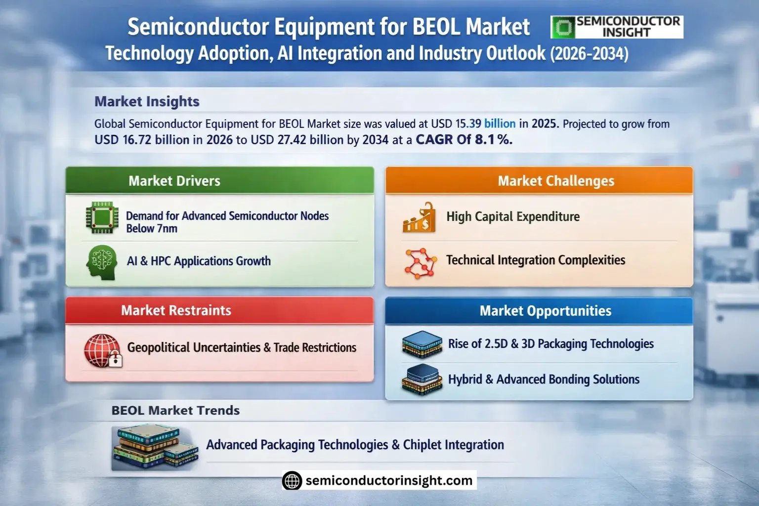
Global Semiconductor Equipment for BEOL Market size was valued at USD 15.39 billion in 2025. The market is projected to grow from USD 16.72 billion in 2026 to USD 27.42 billion by 2034, exhibiting a CAGR of 8.1% during the forecast period.
Semiconductor back-end equipment (BEOL equipment) refers to the collective term for various process and testing tools used from wafer dicing to final chip testing and packaging after front-end manufacturing. These systems transform bare dies into functional, high-reliability chips through processes like wafer-level packaging (WLP), assembly, molding, and end-product validation. The segment is bifurcated into assembly & packaging (A&P) equipment and test equipment.
The market growth is driven by AI chip demand and advanced packaging adoption, with technologies like hybrid bonding and TSV reshaping industry requirements. While Asia-Pacific dominates with over 60% market share, local manufacturers are gradually penetrating high-end segments traditionally controlled by Japanese and American firms.
MARKET DRIVERS
Growing Demand for Advanced Semiconductor Nodes
Semiconductor Equipment for BEOL Market is witnessing significant growth driven by the increasing demand for advanced process nodes below 7nm. As chipmakers push the boundaries of miniaturization, BEOL processes require more sophisticated equipment to handle complex interconnect structures and low-k dielectric materials.
Expansion of AI and HPC Applications
Artificial intelligence and high-performance computing applications are creating substantial demand for BEOL semiconductor equipment. These applications require chips with increasingly dense interconnect architectures, driving investments in advanced deposition, etching, and planarization tools for back-end-of-line processes.
Additionally, the shift toward 3D IC packaging and heterogeneous integration is creating new requirements for BEOL equipment capable of handling through-silicon vias (TSVs) and other advanced packaging technologies.
MARKET CHALLENGES
High Capital Expenditure Requirements
Semiconductor Equipment for BEOL Market faces challenges from the substantial capital investments required for advanced manufacturing tools. A single EUV lithography system for BEOL layers can cost over $150 million, creating significant barriers for smaller foundries.
Other Challenges
Technical Complexities in Material Integration
Developing equipment that can consistently handle new low-k dielectric materials and copper interconnects at shrinking geometries presents ongoing technical challenges for BEOL equipment manufacturers.
MARKET RESTRAINTS
Geopolitical Uncertainties and Trade Restrictions
Semiconductor Equipment for BEOL Market faces restraints from geopolitical tensions and export controls, particularly affecting equipment sales between major regions. These restrictions could potentially slow down the technology adoption curve in certain markets.
MARKET OPPORTUNITIES
Emerging Advanced Packaging Technologies
The growing adoption of 2.5D and 3D packaging technologies presents significant opportunities for BEOL equipment vendors. These emerging packaging approaches require specialized tools for wafer thinning, bonding, and through-silicon via formation that complement traditional BEOL processes.
Semiconductor Equipment for BEOL Market Trends
Advanced Packaging Technologies Driving Market Growth
Semiconductor Equipment for BEOL Market is experiencing significant transformation due to rapid advancements in packaging technologies. Demand for advanced packaging solutions like Chiplet, 2.5D/3D packaging, and hybrid bonding is reshaping equipment requirements. Hybrid bonding systems and thermocompression bonding equipment are seeing particularly strong demand as these technologies become essential for AI chips and high-bandwidth memory applications.
Other Trends
Testing Equipment Gains Strategic Importance
As semiconductor designs grow more complex, testing equipment has evolved from a supporting role to a critical yield management tool. The rising need for comprehensive chip verification in AI and HPC applications is driving double-digit growth in automatic test equipment (ATE) and probe stations. Manufacturers are integrating more test channels and faster processing capabilities to meet these demands.
Asia-Pacific Dominance in BEOL Equipment Market
With over 60% market share, the Asia-Pacific region remains the production hub for semiconductor BEOL processes. China’s aggressive capacity expansion in both OSAT facilities and foundries, combined with policy support for equipment localization, is creating unique growth dynamics. Domestic Chinese equipment makers are making notable progress in mid-range BEOL technologies while gradually entering advanced packaging segments.
Equipment Specialization and Market Segmentation
Semiconductor Equipment for BEOL Market is bifurcating into distinct segments. High-performance tools for advanced packaging are growing at nearly twice the rate of conventional equipment. This divergence reflects fundamental changes in chip architectures, where packaging now contributes significantly to performance rather than just providing protection. Suppliers are responding with more specialized solutions tailored to specific packaging methodologies.
COMPETITIVE LANDSCAPE
Key Industry Players
Advanced packaging technologies and AI chip demand reshaping BEOL equipment market dynamics
Semiconductor Equipment for BEOL Market is dominated by established players like Applied Materials, ASMPT, and Lam Research, which hold significant shares in packaging and process equipment segments. The competitive landscape is experiencing rapid transformation with the shift toward advanced packaging technologies like 2.5D/3D packaging and hybrid bonding, creating opportunities for specialized equipment providers. Leading companies are actively expanding their portfolios through strategic acquisitions and R&D investments to address the growing demand from AI chip manufacturers and HBM producers.
Niche players like DISCO, Towa Corporation, and Kulicke & Soffa are gaining traction in specific segments such as wafer dicing saws and die attach equipment. Chinese manufacturers including Changchuan Technology and Beijing Huafeng Test & Control are emerging as significant regional players, particularly in the test equipment segment, though they currently focus primarily on mid-range market segments. The market is also seeing increased competition from Korean and Japanese specialists in precision bonding and wafer-level packaging equipment.
List of Key Semiconductor BEOL Equipment Companies Profiled
- Applied Materials
- ASMPT
- Lam Research
- Advantest
- Cohu
- Tokyo Seimitsu (Accretech)
- Teradyne
- FormFactor
- Kulicke & Soffa
- DISCO Corporation
- Towa Corporation
- SUSS MicroTec
- Hangzhou Changchuan Technology
- Beijing Huafeng Test & Control Technology
- Besi
Segment Analysis:
| Segment Category | Sub-Segments | Key Insights |
| By Type |
|
Assembly & Packaging Equipment
|
| By Application |
|
OSAT Providers
|
| By End User |
|
AI Chip Manufacturers
|
| By Technology |
|
Advanced Packaging (2.5D/3D)
|
| By Equipment Function |
|
Final Test Equipment
|
Regional Analysis: Semiconductor Equipment for BEOL Market
Asia-Pacific
Taiwan accounts for over 60% of global foundry capacity, with TSMC driving BEOL equipment demand through advanced packaging solutions like InFO and CoWos. The dense supplier ecosystem around Hsinchu Science Park creates a competitive advantage for equipment testing and adoption.
Samsung and SK Hynix prioritize BEOL equipment innovations for high-bandwidth memory production. The country’s strong materials science capabilities support development of advanced BEOL deposition and etching technologies tailored for 3D NAND architectures.
Chinese semiconductor fabs are rapidly adopting domestic BEOL equipment with government support. SMIC and Yangtze Memory Technologies drive demand for localized deposition and inspection tools, though technology still lags behind international leaders in precision and reliability.
Japanese suppliers dominate niche BEOL segments including advanced packaging materials and precision bonding equipment. Companies like Tokyo Electron and Screen maintain leadership in critical clean process technologies essential for next-generation BEOL applications.
North America
North America remains a key innovation hub for semiconductor equipment for BEOL technologies, with strong R&D centers from Applied Materials, Lam Research, and KLA. The region focuses on developing AI-optimized BEOL processes for next-gen chips, particularly in advanced packaging solutions. Major IDMs like Intel drive equipment requirements for heterogeneous integration, while fabless companies influence BEOL tool specifications through design-technology co-optimization demands.
Europe
Europe maintains strength in specialized BEOL equipment for automotive and industrial applications, with ASML’s EUV lithography being critical for advanced BEOL layers. The region sees growing investment in equipment for power semiconductors and MEMS packaging. IMEC’s research collaborations help shape BEOL equipment roadmaps, particularly for sustainable manufacturing processes and materials.
Middle East & Africa
The MEA region shows emerging potential in semiconductor equipment for BEOL applications through strategic investments in technology transfer partnerships. Countries like Israel develop specialized BEOL solutions for optoelectronics, while UAE initiatives aim to create semiconductor manufacturing ecosystems with focus on advanced packaging technologies.
South America
South America’s semiconductor equipment for BEOL market remains nascent but shows growth through academic-industry collaborations in Brazil and Mexico. Local demand concentrates on BEOL tools for automotive and consumer electronics assembly, with increasing interest in developing regional supply chains for semiconductor back-end manufacturing.
Report Scope
This market research report provides a comprehensive analysis of the Semiconductor Equipment for BEOL Market, covering the forecast period 2025–2034. It offers detailed insights into market dynamics, technological advancements, competitive landscape, and key trends shaping the industry.
Key focus areas of the report include:
- Market Overview: The report begins with an overview outlining its current market scenario, key growth indicators, and industry transformation drivers. It discusses macroeconomic factors, demand-supply balance, regulatory landscape, and the strategic role of semiconductors in powering advancements across industries such as automotive, telecommunications, consumer electronics, and industrial automation.
- Market Size & Forecast: Historical data and future projections for revenue, unit shipments, and market value across major regions and segments.
- Segmentation Analysis: Detailed breakdown by product type, technology, application, and end-user industry to identify high-growth segments and investment opportunities.
- Regional Insights: Insights into market performance across North America, Europe, Asia-Pacific, Latin America, and the Middle East & Africa, including country-level analysis where relevant.
- Competitive Landscape: Profiles of leading market participants, including their product offerings, R&D focus, manufacturing capacity, pricing strategies, and recent developments such as mergers, acquisitions, and partnerships.
- Technology Trends & Innovation: Assessment of emerging technologies, integration of AI/IoT, semiconductor design trends, fabrication techniques, and evolving industry standards.
- Market Drivers & Restraints: Evaluation of factors driving market growth along with challenges, supply chain constraints, regulatory issues, and market-entry barriers.
- Stakeholder Insights: Insights for component suppliers, OEMs, system integrators, investors, and policymakers regarding the evolving ecosystem and strategic opportunities.
Primary and secondary research methods are employed, including interviews with industry experts, data from verified sources, and real-time market intelligence to ensure the accuracy and reliability of the insights presented.
FREQUENTLY ASKED QUESTIONS:
What is the current market size of Semiconductor Equipment for BEOL Market?
-> Semiconductor Equipment for BEOL Market size was valued at USD 15.39 billion in 2025. The market is projected to grow from USD 16.72 billion in 2026 to USD 27.42 billion by 2034, exhibiting a CAGR of 8.1% during the forecast period.
What is the growth rate of the Semiconductor Equipment for BEOL Market?
-> The market is expected to grow at a CAGR of 8.1% during the forecast period (2025-2034).
What are the key segments in the Semiconductor Equipment for BEOL Market?
-> The market is segmented by Process (Test Equipment, Assembly and Packaging Equipment) and by Type (ATE, Test Handler, Probe Station, Wafer Thinning Machine, Wafer Dicing Saw, Die Attach, Molding Machine, Trim and Form Machine, Electroplating Equipment, Others).
Which region dominates the Semiconductor Equipment for BEOL Market?
-> The Asia-Pacific region dominates the global market, with mainland China and Taiwan collectively holding over 60% market share in 2024.
What are the key growth drivers for the Semiconductor Equipment for BEOL Market?
-> Key growth drivers include demand for AI chips and high-bandwidth memory (HBM), advanced packaging technologies (Chiplet, 2.5D/3D packaging), and capacity expansions by OSAT providers and foundries.
Get Sample Report PDF for Exclusive Insights
Report Sample Includes
- Table of Contents
- List of Tables & Figures
- Charts, Research Methodology, and more...