
Engineered Substrate (QST, GaN-on-Si) Market Insights
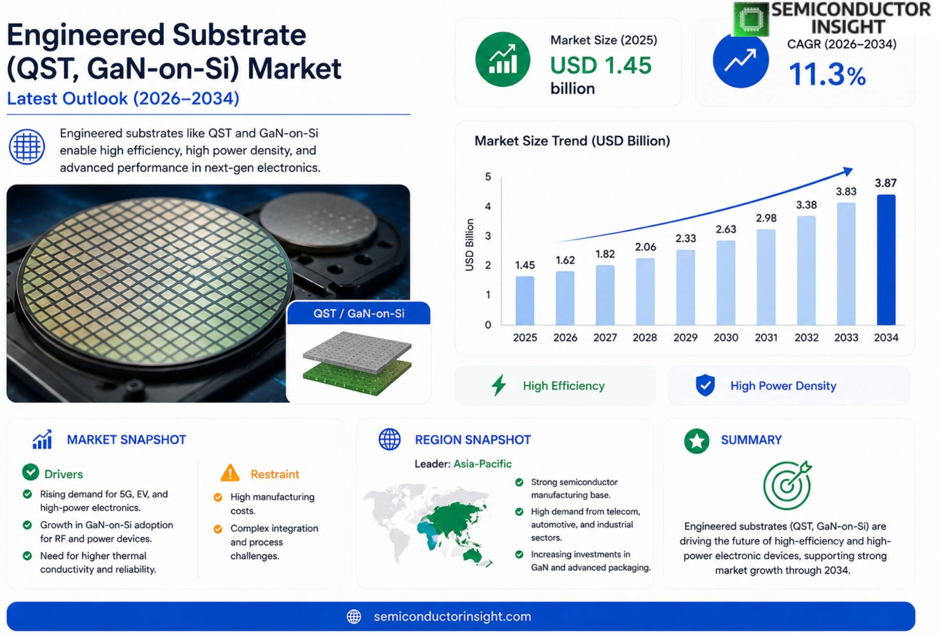
Global Engineered Substrate (QST, GaN-on-Si) Market size was valued at USD 1.45 billion in 2025. The market is projected to grow from USD 1.62 billion in 2026 to USD 3.87 billion by 2034, exhibiting a CAGR of 11.3% during the forecast period.
Engineered substrates, particularly QST (Quasi-Single-Crystal Technology) and GaN-on-Si (Gallium Nitride on Silicon), represent advanced materials designed to enhance performance in high-power and high-frequency electronic applications. These substrates serve as foundational layers for semiconductor devices, enabling superior thermal management, reduced lattice mismatch, and improved efficiency in power electronics, RF amplifiers, and LED technologies. While GaN-on-Si leverages silicon’s cost-effectiveness and scalability for gallium nitride epitaxy, QST substrates offer exceptional thermal conductivity and mechanical stability, making them ideal for demanding environments such as electric vehicles (EVs), 5G infrastructure, and renewable energy systems.
The rapid expansion of Engineered Substrate (QST, GaN-on-Si) Market is driven by surging demand for energy-efficient solutions across industries. For instance, the proliferation of 5G networks has intensified the need for high-performance RF components, where GaN-based devices outperform traditional silicon alternatives. Furthermore, the automotive sector’s shift toward electrification has accelerated adoption of these substrates in EV power modules due to their ability to handle higher voltages and temperatures. Strategic collaborations among key players,such as Soitec’s partnership with GlobalFoundries to develop next-generation QST wafers,are further propelling innovation. Companies like IQE plc, Sumitomo Electric Industries, Ltd., and NGK Insulators are leading the charge with diversified portfolios tailored to emerging applications.
MARKET DRIVERS
Rising Demand for Energy Efficient Power Electronics
The global Engineered Substrate market is witnessing robust expansion due to the growing necessity for higher power density and efficiency in consumer electronics. As system integrators seek to reduce energy consumption, the adoption of GaN-on-Si and Quantum Substrate Technology (QST) solutions has accelerated. These engineered substrates allow for significant improvements in thermal conductivity and electrical performance, driving demand across automotive and industrial sectors. Analysts project that this focus on sustainability will sustain the positive momentum of Engineered Substrate (QST, GaN-on-Si) Market over the next decade.
Miniaturization Trends in RF and Microwave Applications
Another key driver is the relentless push towards smaller and smaller form factors in satellite communications and radar systems. Engineered substrates provide the necessary mechanical rigidity and electrical isolation required for high-frequency operation without compromising signal integrity. The trend towards integrated circuits that require advanced packaging solutions is creating a favorable landscape for Engineered Substrate (QST, GaN-on-Si) Market, particularly in defense and aerospace verticals where performance is paramount.
➤ Market consolidation is observed as key players acquire technology patents to secure their position in the high-performance substrates segment.
Furthermore, the cost reduction associated with silicon-wafer compatibility offers a significant competitive advantage over traditional III-Nitride epitaxial growth processes, making GaN-on-Si particularly attractive for mass-market consumer electronics.
MARKET CHALLENGES
Yield Variability in Wafer Fabrication
The production of QST and advanced GaN-on-Si wafers faces significant technical hurdles regarding defect density and uniformity. Maintaining high yields during the deposition of high-quality compound semiconductor layers on silicon substrates remains a complex process. These manufacturing intricacies pose a challenge to the scalability of Engineered Substrate (QST, GaN-on-Si) Market, as cost-effective mass production requires near-perfect defect management. Manufacturers are investing heavily in process optimization to mitigate these yield gaps.
Other Challenges
Thermal Management Complexity
While Engineered Substrates offer improved thermal paths, managing the heat flux generated by high-power density devices is still a critical hurdle.
High Initial Capital Expenditure
Establishing the infrastructure for epitaxial growth and substrate processing requires substantial investment, which can be a barrier to entry for new competitors aiming to disrupt Engineered Substrate (QST, GaN-on-Si) Market.
MARKET RESTRAINTS
Alternative Material Competition (SiC)
The availability of Silicon Carbide (SiC) as a direct alternative for high-power applications constitutes a potential restraint for the Engineered Substrate market. While SiC offers superior breakdown voltage and thermal conductivity, its cost per watt is often higher than silicon-based solutions. This economic dynamic forces developers to carefully balance performance requirements against budget constraints, slowing the transition to all-GaN-based systems in the lower voltage ranges typically served by Engineered Substrates.
MARKET OPPORTUNITIES
Electric Vehicle and Renewable Energy Integration
The intersection of electric vehicles (EVs) and renewable energy infrastructure presents massive growth potential for the engineered substrate sector. The rising adoption of fast chargers and grid-tied inverters creates a surge in demand for gallium nitride devices capable of handling high power with low loss. As the world moves towards electrification, the demand for reliable Engineered Substrate (QST, GaN-on-Si) Market solutions in power conversion stages is projected to expand significantly.
Miniaturization in IoT and Portable Electronics
With the explosion of the Internet of Things (IoT), there is a pressing need for power management solutions that are both small and efficient. Engineered substrates facilitate the integration of GaN technology into mobile devices and smart wearables. This drive towards ubiquitous connectivity offers a lucrative opportunity for Engineered Substrate (QST, GaN-on-Si) Market to capture greater volume in the consumer electronics supply chain.
Trends
5G Infrastructure Expansion
The rapid global expansion of digital communication networks is fundamentally reshaping the landscape for Engineered Substrate (QST, GaN-on-Si) Market. As industries strive for energy-efficient electronic solutions, the demand for substrates offering superior thermal management and reduced lattice mismatch is surging. These engineered materials serve as the foundational layer for advanced semiconductor devices, enabling enhanced performance in RF amplifiers and LED technologies. The proliferation of next-generation smart grids and high-frequency mobile infrastructure creates a robust environment for market growth, driven by the critical need for components that can handle high-power applications with minimal thermal loss.
Other Trends
Automotive Electrification Drivers
The transition toward full electrification in the automotive sector is a major catalyst for innovation within this industry. As electric vehicles require power modules capable of withstanding higher voltages and temperatures, the scalability and cost-effectiveness of GaN-on-Si technology are becoming increasingly vital. This adoption ensures that engineers can develop efficient and reliable power systems suitable for modern EVs, positioning these substrates as essential components in the ongoing shift away from traditional combustion engines and fossil-fuel-based electricity generation.
Advancements in Quasi-Single-Crystal Technology
Innovation in Quasi-Single-Crystal technology is establishing new benchmarks for thermal conductivity and mechanical stability in the market. QST substrates offer exceptional physical properties that make them ideal for demanding environments, such as renewable energy systems and industrial power machinery. The commercialization of these next-generation wafers is being accelerated by strategic collaborations among key technology leaders, ensuring that the market can reliably support the complex requirements of high-frequency power electronics and advanced communication infrastructure.
COMPETITIVE LANDSCAPE
Key Industry Players
Global Market Evolution and Strategic Dynamics
Engineered Substrate (QST, GaN-on-Si) Market is witnessing robust expansion driven by the surging demand for advanced semiconductor materials. QST technologies and GaN-on-Si are becoming pivotal as foundational layers for high-power and high-frequency applications that require superior thermal management and reduced lattice mismatch. As industries prioritize efficiency in power electronics and RF amplifiers, the increasing adoption of these substrates is facilitating market growth.
Key players in this space are heavily investing in research initiatives to enhance wafer quality and scalability for electric vehicles and renewable energy systems. Strategic collaborations among leading manufacturers are driving innovation, specifically in solutions tailored to meet the rigorous demands of 5G infrastructure and high-voltage applications.
List of Key Engineered Substrate Companies Profiled
- Soitec
- IQE plc
- GlobalFoundries
- Sumitomo Electric Industries
- NGK Insulators
- Transphorm
- TE Connectivity
- Cree
- Wolfspeed
- Texas Instruments
- IXYS
- Infineon Technologies
Segment Analysis:
| Segment Category | Sub-Segments | Key Insights |
| By Type |
|
Leading Segment The market is bifurcated between QST and GaN-on-Si technologies where QST substrates are gaining traction due to their exceptional thermal conductivity and mechanical stability which are critical for handling the thermal loads in high-performance applications. In contrast GaN-on-Si remains dominant due to its cost-effectiveness and compatibility with existing CMOS fabrication lines fostering quicker adoption in the commercial sector. |
| By Application |
|
Leading Segment Applications are dominated by power electronics and radio frequency systems as the proliferation of 5G infrastructure has created a massive demand for gallium nitride RF power amplifiers that offer higher efficiency and linearity compared to incumbent technologies. Additionally, the automotive sector’s electrification trend is driving the use of these substrates in on-board chargers and DC-DC converters to enhance vehicle efficiency. |
| By End User |
|
Leading Segment End-user industries are primarily driven by automotive and telecommunications verticals, where the rapid shift towards electric vehicles necessitates components that can sustain high voltages and temperatures. Meanwhile, the explosion of data centers is fueling the need for high-frequency devices in the telecom sector creating a synergistic demand environment where substrate performance directly dictates system reliability and operational costs. |
| By Wafer Size |
|
Leading Segment Wafer size specifications reveal a clear industry trend towards larger dimensions for improved throughput. While 4-inch wafers currently hold a significant market share manufacturers are aggressively advancing towards 6-inch and 8-inch production capabilities driven by the necessity to reduce per-unit costs and meet the increasing volume demands of mass-market semiconductor fabrication. |
| By Performance Category |
|
Leading Segment Performance specifications are increasingly prioritizing thermal resistance and lattice match quality as developers move beyond basic material properties to emphasize the seamless integration of these substrates into complex power modules. The focus remains on optimizing the interface engineering to minimize dislocations thereby enhancing the overall efficiency and longevity of gallium nitride-based devices in harsh operating environments. |
Regional Analysis: Engineered Substrate (QST, GaN-on-Si) Market
The transition from traditional sputtered AlN films to sputtered aluminum dielectric stacks in QST substrates is revolutionizing circuit performance. This technological jump significantly reduces dielectric loss and thermal resistance, providing a critical advantage in high-frequency RF applications that demand maximum signal integrity and minimal power waste. Development teams prioritize yield improvements in manufacturing these dielectric layers to ensure consistent connectivity standards.
Strategic supply chain adjustments are currently crucial for maintaining stability in the engineered substrate ecosystem. Manufacturers are establishing localized production hubs to mitigate exposure to geopolitical volatility. This localized approach secures a steady flow of raw materials essential for GaN-on-Si wafer processing, fostering a more robust environment for long-term growth.
A distinct shift is occurring where power electronics applications now outpace RF uses in substrate demand. Electric vehicle inverters and industrial motor drives require the high breakdown voltage capabilities inherent to advanced substrate layers. This trend highlights the material’s versatility beyond telecommunications, emphasizing thermal efficiency in heavy industrial machinery.
To maintain competitiveness, leading industry participants are adopting vertical integration strategies. By controlling the supply chain from silicon wafer production to packaged chips, companies aim to optimize costs associated with GaN-on-Si manufacturing. This strategic alignment allows for greater agility in responding to fluctuating global demand patterns while ensuring quality control.
Europe
Europe is witnessing steady growth Engineered Substrate (QST, GaN-on-Si) Market, primarily anchored by the automotive industry. The push for energy-efficient electric mobility solutions in Germany and Scandinavia drives the demand for high-voltage power devices leveraging gallium nitride layers. Regulatory policies favoring green energy production further accelerate the adoption of these efficient substrates. The region is also prioritizing the development of eco-friendly semiconductor manufacturing processes to complement the technical advantages of QST materials in smart grid applications.
Asia-Pacific
Asia-Pacific presents the most dynamic environment for Engineered Substrate (QST, GaN-on-Si) Market, characterizing the highest volume of 5G infrastructure deployment. Countries like South Korea and Taiwan are investing heavily in foundry capacity to meet the surging need for compact RF components. The region benefits from established silicon manufacturing ecosystems that facilitate seamless transition to GaN-on-Si technologies. The competitive pressure in this market drives continuous innovation to lower costs and accelerate time-to-market for next-generation power amplifiers.
South America
South America is emerging as a promising frontier for Engineered Substrate (QST, GaN-on-Si) Market, with Brazil taking the lead in industrial automation. Local manufacturers are beginning to integrate high-performance transistor options to upgrade aging power grids, seeking to improve operational efficiency. The focus remains on cost-effective adoption of substrate technology to support sustainable development initiatives. As the region digitizes, the need for reliable signal processing in industrial hardware will likely see a significant uptick in demand for high-frequency substrates.
Middle East & Africa
The Middle East and Africa are focusing on expanding the reach of Engineered Substrate (QST, GaN-on-Si) Market through telecom infrastructure modernization projects. Significant capital inflows are being directed toward building resilient data centers capable of supporting advanced computing. The demand is slowly shifting from basic consumption to specialized industrial control systems requiring stable dielectric layers. Strategic initiatives are underway to localize tech capabilities, reducing reliance on imported components and fostering technological self-sufficiency.
Report Scope
This market research report provides a comprehensive analysis of the Engineered Substrate (QST, GaN-on-Si) Market , covering the forecast period 2026–2034. It offers detailed insights into market dynamics, technological advancements, competitive landscape, and key trends shaping the industry.
Key focus areas of the report include:
- Market Overview: The report begins with an overview outlining its current market scenario, key growth indicators, and industry transformation drivers. It discusses macroeconomic factors, demand–supply balance, regulatory landscape, and the strategic role of semiconductors in powering advancements across industries such as automotive, telecommunications, consumer electronics, and industrial automation.
- Market Size & Forecast: Historical data and future projections for revenue, unit shipments, and market value across major regions and segments.
- Segmentation Analysis: Detailed breakdown by product type, technology, application, and end-user industry to identify high-growth segments and investment opportunities.
- Regional Insights: Insights into market performance across North America, Europe, Asia-Pacific, Latin America, and the Middle East & Africa, including country-level analysis where relevant.
- Competitive Landscape: Profiles of leading market participants, including their product offerings, R&D focus, manufacturing capacity, pricing strategies, and recent developments such as mergers, acquisitions, and partnerships.
- Technology Trends & Innovation: Assessment of emerging technologies, integration of AI/IoT, semiconductor design trends, fabrication techniques, and evolving industry standards.
- Market Drivers & Restraints: Evaluation of factors driving market growth along with challenges, supply chain constraints, regulatory issues, and market-entry barriers.
- Stakeholder Insights: Insights for component suppliers, OEMs, system integrators, investors, and policymakers regarding the evolving ecosystem and strategic opportunities.
Primary and secondary research methods are employed, including interviews with industry experts, data from verified sources, and real-time market intelligence to ensure the accuracy and reliability of the insights presented.
FREQUENTLY ASKED QUESTIONS:
What is the current market size of Engineered Substrate (QST, GaN-on-Si) Market?
-> Engineered Substrate (QST, GaN-on-Si) Market was valued at USD 1.45 billion in 2025 and is projected to reach USD 3.87 billion by 2034, exhibiting a CAGR of 11.3%.
Which key companies operate Engineered Substrate (QST, GaN-on-Si) Market?
-> Key players include IQE plc, Sumitomo Electric Industries, Ltd., NGK Insulators, Soitec, and GlobalFoundries.
What are the key growth drivers?
-> Key growth drivers include the need for energy-efficient solutions, proliferation of 5G networks, automotive shift towards electrification, and strategic R&D partnerships between companies.
Which region dominates the market?
-> Global demand is surging due to the implementation of these solutions across automotive and telecommunications sectors.
What are the emerging trends?
-> Emerging trends include electric vehicle (EV) power modules, 5G infrastructure, and renewable energy systems.

Get Sample Report PDF for Exclusive Insights
Report Sample Includes
- Table of Contents
- List of Tables & Figures
- Charts, Research Methodology, and more...
 Download Sample Report PDF


