
Defect Inspection (E-beam, Laser) System Market Insights
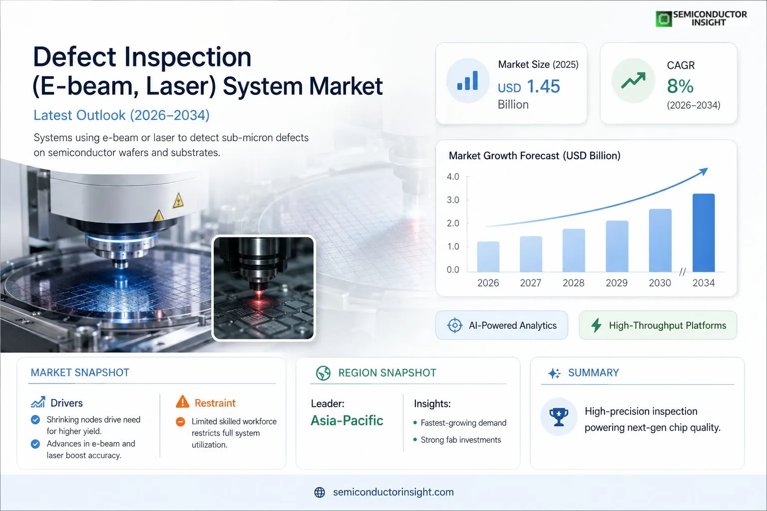
Global Defect Inspection (E-beam, Laser) System market size was valued at USD 1.45 billion in 2025. The market is projected to grow from USD 1.53 billion in 2025 to USD 3.07 billion by 2034, exhibiting a CAGR of 8% during the forecast period.
Defect inspection systems employ high‑energy electron beams or precision lasers to detect sub‑micron flaws on semiconductor wafers, photomasks and advanced packaging substrates, enabling manufacturers to maintain yield and reliability.The market accelerates because of surging demand for advanced nodes, increased adoption of EUV lithography and tighter quality standards across automotive and IoT chips.
Key players such as KLA Corp., Applied Materials, Hitachi High‑Technologies and ASML’s inspection division are expanding portfolios through AI‑driven analytics and recently launched high‑throughput e‑beam platforms.
MARKET DRIVERS
Rising Demand for Semiconductor Yield Improvement
Defect Inspection (E-beam, Laser) System Market is being propelled by manufacturers’ need to achieve higher wafer yields. As device geometries shrink, even sub‑micron defects can cause functional failures, prompting fabs to invest in advanced inspection solutions that detect and classify defects early in the process.
Advancements in E‑beam and Laser Technologies
Recent improvements in beam stability and laser pulse precision have increased detection accuracy while reducing inspection time. These technological gains enable operators to monitor critical layers without compromising throughput, a critical factor for high‑volume production lines.
➤ Integrated inspection platforms that combine e‑beam and laser modalities are shortening defect‑to‑repair cycles, thereby boosting overall equipment effectiveness.
Manufacturers are also recognizing the long‑term cost benefits of proactive defect management. By minimizing scrap and re‑work, companies can preserve margin even in a highly competitive market landscape.
MARKET CHALLENGES
High Capital Expenditure
The upfront investment required for state‑of‑the‑art e‑beam and laser inspection systems remains substantial. Smaller fabs and emerging players often face financing constraints, which can delay adoption despite clear performance advantages.
Other Challenges
Technical Complexity
Operating and maintaining high‑resolution inspection equipment demands specialized knowledge. The learning curve for calibration, data interpretation, and software integration can hinder rapid deployment across diverse manufacturing environments.
MARKET RESTRAINTS
Limited Skilled Workforce
There is a shortage of engineers proficient in both semiconductor process technology and advanced inspection instrumentation. This talent gap restricts the ability of fabs to fully exploit the capabilities of Defect Inspection (E-beam, Laser) System Market solutions, leading to underutilization of existing assets.
MARKET OPPORTUNITIES
Emerging Memory and Packaging Applications
New memory architectures such as 3D NAND and advanced packaging formats are creating fresh inspection requirements. The ability of e‑beam and laser systems to resolve three‑dimensional defect structures positions them as essential tools for next‑generation product lines, opening significant growth avenues for vendors.
Defect Inspection (E-beam, Laser) System Market Trends
Rising Demand for Sub‑Micron Inspection in Advanced Nodes
The acceleration of semiconductor scaling toward sub‑45 nm nodes has intensified the need for precise defect detection. High‑energy electron beams and finely tuned laser systems are now essential for identifying sub‑micron flaws on wafers, photomasks, and advanced packaging substrates. OEMs in automotive and IoT segments are imposing tighter quality standards, prompting fabs to adopt inspection solutions that can keep pace with increased throughput requirements. This shift is also supported by broader adoption of EUV lithography, which demands higher defect control to maintain yield across complex patterning steps. As a result, equipment suppliers are prioritizing upgrades that deliver both higher resolution and faster scan rates, ensuring that yield loss remains minimal even as design complexity grows.
Other Trends
AI‑Driven Analytics Elevate Yield Management
Artificial‑intelligence algorithms are being embedded directly into inspection platforms to automate defect classification and root‑cause analysis. By correlating defect signatures with process parameters, AI reduces manual review time and improves predictive maintenance scheduling. Leading vendors have introduced cloud‑enabled dashboards that aggregate data from multiple e‑beam and laser units, offering real‑time insights that help line engineers adjust process windows before yield degradation becomes significant. This data‑centric approach not only shortens cycle time but also creates a feedback loop that drives continuous improvement across the manufacturing line.
Consolidation of Inspection Platforms with High‑Throughput e‑Beam Solutions
Recent product launches focus on consolidating multiple inspection functions into a single high‑throughput e‑beam system. These platforms combine defect detection, metrology, and layer‑stack verification, reducing floor space and capital expenditure. The emphasis on throughput aligns with the growing volume of wafers processed in 300 mm fabs, where cycle time is a critical cost driver. Manufacturers are also integrating laser‑based modules for rapid surface scanning, complementing the deeper penetration capabilities of electron beams. This hybrid strategy enables fabs to balance speed and resolution, delivering comprehensive defect coverage while maintaining the high productivity demanded by modern semiconductor roadmaps.
COMPETITIVE LANDSCAPEKey Industry Players
Competitive Landscape of the Global Defect Inspection (E-beam, Laser) System Market
Defect Inspection (E-beam, Laser) System Market is dominated by a handful of large technology providers that combine deep semiconductor expertise with advanced metrology capabilities. KLA Corp. leads the segment with its high‑throughput e‑beam platforms and AI‑driven analytics, capturing a substantial share of wafer‑level inspection revenue. Applied Materials follows closely, leveraging its broad equipment portfolio to integrate laser‑based defect detection into front‑end fab lines. ASML’s inspection division and Hitachi High‑Technologies have accelerated growth by launching next‑generation e‑beam and laser tools that address sub‑10 nm node challenges, especially for EUV lithography. Tokyo Electron and Nikon Metrology round out the core tier, offering complementary optical and electron‑beam solutions that appeal to OEMs seeking end‑to‑end yield management across multiple process steps. The market structure reflects a classic oligopoly, where these incumbents set pricing benchmarks and drive technology roadmaps, while maintaining strategic partnerships with foundries and design houses.
Beyond the dominant tier, a diverse set of niche innovators enriches the competitive landscape with specialized capabilities. Onto Innovation and Advantest provide hybrid inspection systems that blend e‑beam precision with rapid laser scanning for advanced packaging substrates. CyberOptics focuses on machine‑vision laser scanners for automotive and IoT chips, emphasizing cost‑effective high‑volume inspection. Bruker and Veeco Instruments target research‑grade e‑beam microscopes for defect analysis in emerging materials. Camtek, SUSS MicroTec, and MKS Instruments contribute focused laser defect detection modules for mask and wafer fab integration. These companies, while smaller in revenue, drive differentiation through rapid product cycles, customizable software stacks, and strong regional customer support, thereby ensuring a vibrant ecosystem that supports the market’s projected 8 % CAGR through 2034.
List of Key Defect Inspection System Companies Profiled
- KLA Corp.
- Applied Materials
- Hitachi High‑Technologies
- ASML Inspection Division
- Tokyo Electron
- Nikon Metrology
- Onto Innovation
- Advantest
- CyberOptics
- Bruker
- Veeco Instruments
- Camtek
- SUSS MicroTec
- MKS Instruments
- Nova Ltd. (Hummingbird)
Segment Analysis:
| Segment Category | Sub-Segments | Key Insights |
| By Type |
|
E-beam Dominant
|
| By Application |
|
Wafer Inspection Leadership
|
| By End User |
|
Foundry Preference
|
| By Process Stage |
|
Post‑Pattern Emphasis
|
| By Market Need |
|
Reliability Assurance Dominates
|
Regional Analysis: North America
United States
The aerospace and defense sector in the United States is a major driver for Defect Inspection (E-beam, Laser) System Market, demanding high levels of precision and reliability in component manufacturing. Stringent safety standards necessitate advanced inspection techniques to identify even minute flaws.
The automotive industry’s pursuit of higher quality and safety standards has led to a substantial adoption of Defect Inspection (E-beam, Laser) System Market in the US. This includes inspecting critical components and welds for defects that could compromise vehicle integrity.
The electronics and semiconductor industries in the United States rely heavily on Defect Inspection (E-beam, Laser) System Market for ensuring the quality and functionality of microchips and electronic components. Precise inspection is crucial at various stages of production.
The medical device sector in the US utilizes Defect Inspection (E-beam, Laser) System Market to guarantee the safety and efficacy of intricate medical instruments and implants. Regulatory compliance and patient safety are paramount in this application.
Europe
Europe presents a diverse market for Defect Inspection (E-beam, Laser) System Market, with varying levels of adoption across different countries. Germany, the UK, and France are key markets driven by strong manufacturing bases and stringent quality regulations. The automotive and aerospace industries in these countries are significant consumers. Business strategies often focus on providing sustainable and energy-efficient inspection solutions, aligning with the region’s environmental concerns. The increasing adoption of Industry 4.0 technologies is also influencing the demand for automated inspection systems across Europe.
Asia-Pacific
The Asia-Pacific region represents the fastest-growing market for Defect Inspection (E-beam, Laser) System Market. China, Japan, and South Korea are leading countries contributing to this growth, fueled by rapid industrialization and increasing demand for high-quality manufactured goods. The electronics, automotive, and aerospace sectors are major drivers. Investment in advanced inspection technologies is rising, particularly in China, to meet stringent domestic standards and global competitiveness.
South America
South America is an emerging market for Defect Inspection (E-beam, Laser) System Market, with growing opportunities in the automotive, aerospace, and mining sectors. Brazil and Argentina are key markets, with increasing investments in manufacturing and infrastructure development. The demand for reliable and cost-effective inspection solutions is rising as industries strive to improve product quality and reduce operational costs.
Middle East & Africa
The Middle East & Africa region is witnessing moderate growth in Defect Inspection (E-beam, Laser) System Market. The aerospace and oil & gas industries in countries like the UAE, Saudi Arabia, and South Africa are key drivers. Increasing investments in infrastructure projects and manufacturing are contributing to the demand for advanced inspection technologies. As industrialization progresses, the market is expected to see further expansion.
Report Scope
This market research report provides a comprehensive analysis of the Defect Inspection (E-beam, Laser) System Market , covering the forecast period 2026–2034. It offers detailed insights into market dynamics, technological advancements, competitive landscape, and key trends shaping the industry.
Key focus areas of the report include:
- Market Overview: The report begins with an overview outlining its current market scenario, key growth indicators, and industry transformation drivers. It discusses macroeconomic factors, demand–supply balance, regulatory landscape, and the strategic role of semiconductors in powering advancements across industries such as automotive, telecommunications, consumer electronics, and industrial automation.
- Market Size & Forecast: Historical data and future projections for revenue, unit shipments, and market value across major regions and segments.
- Segmentation Analysis: Detailed breakdown by product type, technology, application, and end-user industry to identify high-growth segments and investment opportunities.
- Regional Insights: Insights into market performance across North America, Europe, Asia-Pacific, Latin America, and the Middle East & Africa, including country-level analysis where relevant.
- Competitive Landscape: Profiles of leading market participants, including their product offerings, R&D focus, manufacturing capacity, pricing strategies, and recent developments such as mergers, acquisitions, and partnerships.
- Technology Trends & Innovation: Assessment of emerging technologies, integration of AI/IoT, semiconductor design trends, fabrication techniques, and evolving industry standards.
- Market Drivers & Restraints: Evaluation of factors driving market growth along with challenges, supply chain constraints, regulatory issues, and market-entry barriers.
- Stakeholder Insights: Insights for component suppliers, OEMs, system integrators, investors, and policymakers regarding the evolving ecosystem and strategic opportunities.
Primary and secondary research methods are employed, including interviews with industry experts, data from verified sources, and real-time market intelligence to ensure the accuracy and reliability of the insights presented.
FREQUENTLY ASKED QUESTIONS:
What is the current market size of Defect Inspection (E-beam, Laser) System Market?
-> Defect Inspection (E-beam, Laser) System Market was valued at USD 1.45 billion in 2025 and is expected to reach USD 3.07 billion by 2034, representing a CAGR of 8% during the forecast period.
Which key companies operate in Defect Inspection (E-beam, Laser) System Market?
-> Key players include KLA Corp., Applied Materials, Hitachi High‑Technologies, and ASML’s inspection division.
What are the key growth drivers?
-> Key growth drivers include surging demand for advanced nodes, increased adoption of EUV lithography, and tighter quality standards across automotive and IoT chips.
Which region dominates the market?
-> The reference does not specify a dominant region.
What are the emerging trends?
-> Emerging trends include AI‑driven analytics and high‑throughput e‑beam platforms expanding inspection capabilities.

Get Sample Report PDF for Exclusive Insights
Report Sample Includes
- Table of Contents
- List of Tables & Figures
- Charts, Research Methodology, and more...
 Download Sample Report PDF


