
Chiplet Integration Packaging Market Insights
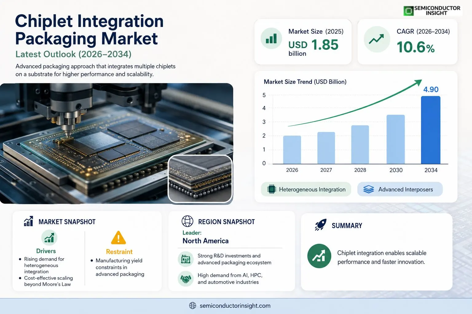
Global chiplet integration packaging market size was valued at USD 1.85 billion in 2025. The market is projected to grow from USD 1.85 billion in 2025 to USD 4. 90 billion by 2034, exhibiting a CAGR of 10·6 % during the forecast period.
Chiplet integration packaging refers to the advanced semiconductor assembly approach that interconnects multiple heterogeneous die,known as chiplets,on a common substrate or interposer using high-density interconnects such as silicon-through-silicon vias (TSVs), micro-bumps or fan-out wafer-level packaging (FOWLP). This technique enables functional specialization, improves yield and accelerates time-to-market for complex system-on-chip solutions.
The market is experiencing rapid expansion because demand for high-performance computing, AI accelerators and heterogeneous system architectures is soaring worldwide; however, challenges related to design complexity and supply-chain coordination persist.
Furthermore, increasing investments by
MARKET DRIVERS
Accelerated Demand for Heterogeneous Integration
Chiplet Integration Packaging Market is being propelled by the need to combine diverse functions,compute, memory, and RF,into a single substrate. System‑level performance gains and reduced time‑to‑market are encouraging OEMs to adopt chiplet‑based architectures.
Cost‑Effective Scaling Beyond Moore’s Law
By reusing proven “chiplets,” manufacturers can sidestep costly mask set revisions, delivering up to 30% lower production expenses while maintaining performance parity with monolithic dies.
➤ Industry surveys indicate that more than 55% of leading semiconductor firms plan to increase chiplet investments by 2025.
Additionally, the rise of AI accelerators and 5G infrastructure creates a robust pipeline of demand, ensuring sustained growth for packaging solutions that support high‑density interconnects.
MARKET CHALLENGES
Standardization and Interoperability Issues
Despite rapid adoption, the lack of universally accepted electrical and mechanical standards hampers seamless integration across suppliers, leading to prolonged design cycles.
Other Challenges
Supply Chain Complexity
Fragmented sources for silicon, interposers, and advanced substrates increase lead times and cost volatility, especially during global shortages.
MARKET RESTRAINTS
Manufacturing Yield Constraints
Advanced chiplet packaging requires precise alignment and bonding at sub‑micron tolerances. Yield losses during the assembly stage can erode the cost benefits that drive adoption.
Thermal Management Challenges
High‑performance chiplets generate significant heat, and inadequate thermal pathways can limit reliability. Designing efficient heat spreaders without increasing package footprint remains a technical hurdle.
MARKET OPPORTUNITIES
Emerging AI and Edge Computing Segments
The surge in AI workloads and edge deployments creates a demand for modular solutions that can be quickly re‑configured. Chiplet integration offers a scalable route to meet varied performance targets while preserving design agility.
Growth of Advanced Interposer Technologies
Innovations in silicon‑photonic and glass interposers enable higher bandwidth and lower latency connections, opening new market niches for high‑speed data centers and autonomous systems.
Chiplet Integration Packaging Market Trends
Rising Demand for Heterogeneous Computing
Chiplet Integration Packaging Market is being reshaped by a surge in heterogeneous system architectures. Leading semiconductor designers are leveraging chiplet‑based assemblies to combine specialized functional blocks,such as AI accelerators, high‑speed interconnects, and memory clusters,on a single substrate. This modular approach shortens development cycles, improves yields, and aligns with the growing need for scalable performance in data‑center processors and edge AI devices. Analysts observe that the flexibility of chiplet integration enables rapid customization for emerging workloads while maintaining a consistent manufacturing footprint.
Other Trends
Managing Design Complexity
Design complexity remains a pivotal concern as Chiplet Integration Packaging Market matures. The integration of multiple heterogeneous dies requires advanced simulation tools, precise alignment of through‑silicon vias, and rigorous verification of electrical and thermal interactions. Companies are investing in co‑design platforms that unify layout, packaging, and system‑level validation, thereby reducing error rates and time to market. Collaborative design ecosystems are emerging, allowing IP providers and OEMs to share validated building blocks, which mitigates risk associated with intricate interconnect schemes.
Standardization and Supply‑Chain Alignment
Another notable development in Chiplet Integration Packaging Market is the push toward industry standards and tighter supply‑chain coordination. Standardized interposer dimensions, pin‑count conventions, and electrical interface specifications are facilitating smoother integration across multiple vendors. This harmonization eases procurement challenges and supports a more resilient component pipeline, especially as global semiconductor supply dynamics evolve. By adopting common design frameworks, manufacturers can achieve economies of scale while preserving the performance benefits inherent to chiplet architectures.
COMPETITIVE LANDSCAPE
Key Industry Players
Chiplet Integration Packaging: Competitive Landscape Overview
Chiplet Integration Packaging Market is dominated by a handful of large semiconductor foundries and advanced‑assembly specialists that can deliver high‑density interconnects such as TSVs, micro‑bumps, and fan‑out wafer‑level packaging. TSMC leads the segment with its CoWoS and InFO offerings, leveraging a massive volume base and deep R&D investment to attract AI accelerator designers and high‑performance computing (HPC) customers. Intel, through its EMIB and Foveros technologies, remains a pivotal player that pushes heterogenous stacking for data‑center processors. ASE Technology Holding and Amkor Technology provide the most extensive contract packaging services, enabling fabless firms to adopt chiplet strategies without building dedicated fabs. Samsung Electronics and GlobalFoundries round out the top tier by offering both foundry capacity and advanced packaging, creating a vertically integrated value chain that shapes market dynamics and pricing structures.
Beyond the core leaders, a diverse set of niche innovators contributes critical capabilities that expand the ecosystem. STMicroelectronics and Infineon focus on automotive‑grade chiplet solutions, emphasizing reliability and long‑term supply. NXP Semiconductors and Qualcomm specialise in mobile‑centric heterogeneous designs, while IBM and Broadcom leverage proprietary interconnect patents to differentiate their offerings. Emerging specialists such as Xperi Holding and TSMC’s partner, IMEC, drive research collaborations that accelerate new materials and design‑for‑assembly methodologies, ensuring the market remains vibrant and competitive.
List of Key Chiplet Integration Packaging Companies Profiled
- TSMC
- Intel
- ASE Technology Holding
- Amkor Technology
- Samsung Electronics
- GlobalFoundries
- STMicroelectronics
- Infineon Technologies
- Qualcomm
- NXP Semiconductors
- IBM
- Broadcom
- Xperi Holding
- IMEC
Segment Analysis:
| Segment Category | Sub-Segments | Key Insights |
| By Type |
|
Logic Chiplets
|
| By Application |
|
AI Accelerators
|
| By End User |
|
Semiconductor Manufacturers
|
| By Integration Technology |
|
Silicon Interposer
|
| By Market Driver |
|
Performance Demand
|
Regional Analysis: North America
North America
The adoption of 2.5D and 3D packaging is gaining momentum, offering enhanced performance and density for advanced semiconductor devices. This trend is fueled by the need to overcome the limitations of traditional 2D scaling, leading to increased focus on chiplet integration and advanced interconnects.
The integration of diverse chiplets with varying functionalities is becoming increasingly important. This strategy allows for optimized performance and efficiency by combining specialized components into a single package. Key areas of focus include seamless integration of memory, logic, and I/O chiplets.
Research and development in advanced packaging materials, such as organic and inorganic interconnects, are crucial for enabling high-speed data transfer and improved thermal management. The development of new die attach materials and thermal interface materials is also a key area of innovation.
Strong collaborations between semiconductor manufacturers, packaging companies, and equipment suppliers are essential for driving innovation and accelerating the adoption of advanced packaging technologies. These partnerships facilitate the development of standardized interfaces and processes.
Europe
Europe represents a significant market for Chiplet Integration Packaging Market, with a strong emphasis on developing a self-sufficient semiconductor ecosystem. Government initiatives are fostering investments in R&D and manufacturing capabilities across the continent. Key areas of focus include automotive semiconductors, industrial applications, and power electronics, where advanced packaging is crucial for performance and reliability. Business strategies in Europe often involve close collaboration with academic institutions and research centers to drive technological advancements and talent development.
Asia-Pacific
Asia-Pacific is experiencing rapid growth in Chiplet Integration Packaging Market, driven by the burgeoning electronics industries in countries like China, Japan, and South Korea. The region’s strong demand for high-performance computing, 5G infrastructure, and consumer electronics is fueling the adoption of advanced packaging technologies. Government support for the semiconductor industry and significant investments in manufacturing capacity are further contributing to the market’s growth.
United States
The United States remains a key player in Chiplet Integration Packaging Market, with significant investments in R&D and manufacturing. Government initiatives, such as the CHIPS Act, are aimed at bolstering the domestic semiconductor industry and promoting innovation in advanced packaging technologies. The focus is on developing cutting-edge packaging solutions for high-performance computing, AI, and defense applications.
South America
South America presents an emerging market for Chiplet Integration Packaging Market, driven by the growth of the electronics and telecommunications sectors. Increasing investments in infrastructure and digitalization are creating demand for advanced packaging solutions in areas such as industrial automation and consumer electronics.
Middle East & Africa
The Middle East & Africa region is an evolving market for Chiplet Integration Packaging Market, with growing investments in technology and infrastructure. The expansion of the telecommunications sector, particularly 5G, is driving demand for advanced packaging solutions in mobile devices and network equipment.
Report Scope
This market research report provides a comprehensive analysis of the Chiplet Integration Packaging Market , covering the forecast period 2026–2034. It offers detailed insights into market dynamics, technological advancements, competitive landscape, and key trends shaping the industry.
Key focus areas of the report include:
- Market Overview: The report begins with an overview outlining its current market scenario, key growth indicators, and industry transformation drivers. It discusses macroeconomic factors, demand–supply balance, regulatory landscape, and the strategic role of semiconductors in powering advancements across industries such as automotive, telecommunications, consumer electronics, and industrial automation.
- Market Size & Forecast: Historical data and future projections for revenue, unit shipments, and market value across major regions and segments.
- Segmentation Analysis: Detailed breakdown by product type, technology, application, and end-user industry to identify high-growth segments and investment opportunities.
- Regional Insights: Insights into market performance across North America, Europe, Asia-Pacific, Latin America, and the Middle East & Africa, including country-level analysis where relevant.
- Competitive Landscape: Profiles of leading market participants, including their product offerings, R&D focus, manufacturing capacity, pricing strategies, and recent developments such as mergers, acquisitions, and partnerships.
- Technology Trends & Innovation: Assessment of emerging technologies, integration of AI/IoT, semiconductor design trends, fabrication techniques, and evolving industry standards.
- Market Drivers & Restraints: Evaluation of factors driving market growth along with challenges, supply chain constraints, regulatory issues, and market-entry barriers.
- Stakeholder Insights: Insights for component suppliers, OEMs, system integrators, investors, and policymakers regarding the evolving ecosystem and strategic opportunities.
Primary and secondary research methods are employed, including interviews with industry experts, data from verified sources, and real-time market intelligence to ensure the accuracy and reliability of the insights presented.
FREQUENTLY ASKED QUESTIONS:
What is the current market size of Chiplet Integration Packaging Market?
-> Chiplet Integration Packaging Market was valued at USD 1.85 billion in 2025 and is expected to reach USD 4.90 billion by 2034, exhibiting a CAGR of 10.6% during the forecast period.
Which key companies operate in Chiplet Integration Packaging Market?
-> Key players include Intel Corporation, Advanced Micro Devices (AMD), Taiwan Semiconductor Manufacturing Company (TSMC), Samsung Electronics, GlobalFoundries, and Nvidia Corporation, among others.
What are the key growth drivers?
-> Key growth drivers include rising demand for high‑performance computing, AI accelerator deployment, heterogeneous system architectures, and the push for modular chip designs to improve yield and time‑to‑market.
Which region dominates the market?
-> Asia‑Pacific is the fastest‑growing region, while North America remains a dominant market due to significant semiconductor R&D investments.
What are the emerging trends?
-> Emerging trends include advanced silicon interposers, fan‑out wafer‑level packaging (FOWLP) for chiplets, integration of photonic interconnects, and the development of standardized chiplet ecosystems.

Get Sample Report PDF for Exclusive Insights
Report Sample Includes
- Table of Contents
- List of Tables & Figures
- Charts, Research Methodology, and more...
 Download Sample Report PDF

