
Atomic Layer Etch (ALE) Market Insights
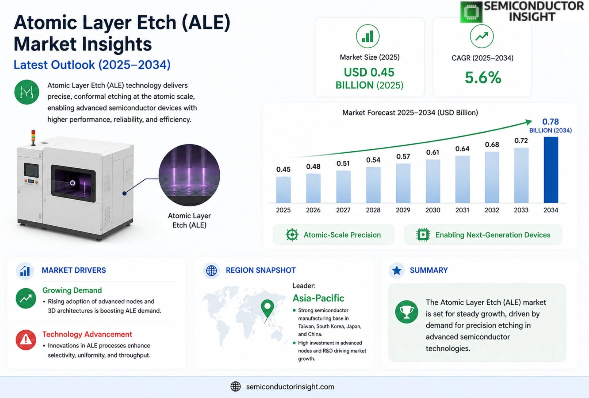
Global Atomic Layer Etch (ALE) Market size was valued at USD 0.45 billion in 2025. The market is projected to grow from USD 0.48 billion in 2026 to USD 0.78 billion by 2034, exhibiting a CAGR of 5.6% during the forecast period.
Atomic Layer Etch (ALE) is a precision plasma‑based etching technology that removes material one atomic layer at a time, delivering sub‑nanometer control of critical dimensions while minimizing damage,an essential capability for advanced semiconductor nodes below 10 nm.
The market is experiencing rapid growth because semiconductor manufacturers are scaling down device architectures, driving demand for high‑selectivity etching solutions; however, high equipment costs pose challenges. Furthermore, increased investment in logic and memory chips, together with the rollout of EUV lithography, fuels adoption of ALE processes. Key players such as Lam Research, Tokyo Electron Limited and Applied Materials are expanding their ALE portfolios through strategic collaborations and technology roadmaps.
MARKET DRIVERS
Advanced Semiconductor Scaling
The relentless push for sub‑10 nm device architectures is compelling manufacturers to adopt precise etching solutions. Atomic Layer Etch (ALE) Market technologies deliver monolayer control, enabling high‑aspect‑ratio features without damaging underlying layers, which is critical for next‑generation logic and memory chips.
Demand for 3D Integration
Three‑dimensional packaging and heterogeneous integration require selective removal of materials in confined spaces. The conformal nature of ALE processes reduces defectivity, supporting the growth of 3D‑IC and system‑in‑package markets. Manufacturers are therefore prioritizing ALE over traditional plasma etching.
➤ “Precision etching is becoming the linchpin for Moore’s Law continuation, and ALE is the most reliable pathway.”
Regulatory pressure for lower power consumption further accelerates adoption, as ALE enables thinner dielectric layers while maintaining reliability, directly contributing to reduced energy usage in data centers and mobile devices.
MARKET CHALLENGES
Process Integration Complexity
Integrating ALE steps into established fab lines often requires new precursor chemistries and temperature windows, creating a steep learning curve. The need for specialized equipment can delay ramp‑up and increase capital expenditures.
Other Challenges
Equipment Cost
High‑precision ALE reactors are priced above conventional etchers, making ROI assessments critical for smaller fabs.
MARKET RESTRAINTS
Limited Precursor Availability
The niche nature of ALE chemistry means that suitable precursors are produced by a limited number of suppliers, leading to potential supply chain bottlenecks. This scarcity can constrain production scaling and increase material costs.
MARKET OPPORTUNITIES
Emerging Applications in Quantum Devices
Quantum computing components demand ultra‑clean interfaces and atomically precise patterning. ALE’s ability to etch without introducing damage positions it as a strategic enabler for quantum chip manufacturing, opening new revenue streams.
Expansion into Advanced Packaging
As advanced packaging gains market share, the need for selective removal of barrier layers and redistribution layers creates a fertile ground for ALE solutions. Companies that develop turnkey ALE platforms for packaging are likely to capture significant market share.
Trends
Scaling of Semiconductor Nodes Drives ALE Adoption
The shift toward sub‑10 nm device architectures has intensified the need for atomic‑scale precision in pattern transfer. Precision plasma‑based etching, embodied by the Atomic Layer Etch (ALE) approach, enables removal of material one atomic layer at a time, delivering sub‑nanometer control while limiting plasma damage. Semiconductor manufacturers targeting advanced logic and memory chips increasingly integrate ALE processes to meet tighter critical dimension tolerances and to support the rollout of extreme ultraviolet (EUV) lithography. This alignment of technology roadmaps creates a sustainable demand cycle for ALE solutions, reinforcing the overall market momentum without relying on explicit growth percentages.
Other Trends
Cost Management and Equipment Investment
Although ALE delivers unmatched selectivity and precision, the capital intensity of dedicated plasma reactors presents a notable barrier for mid‑size fabs. Companies are responding by offering modular equipment configurations and leasing models that spread upfront costs over longer periods. Concurrently, manufacturers are consolidating equipment purchases across multiple process steps, leveraging shared infrastructure to improve ROI. These financing strategies help mitigate the impact of high equipment prices while preserving the technical advantages that ALE provides.
Strategic Partnerships Expand Technology Portfolio
Leading equipment suppliers such as Lam Research, Tokyo Electron Limited, and Applied Materials are pursuing collaborative agreements with specialty material firms and research institutions. These partnerships accelerate the introduction of new precursor chemistries, improve selectivity for high‑k/metal gate stacks, and broaden the applicability of ALE across both front‑end and back‑end processes. By integrating complementary technologies,such as atomic layer deposition (ALD) and plasma‑enhanced ALD,partners create end‑to‑end solutions that streamline integration and reduce cycle time. The collective effort strengthens Atomic Layer Etch (ALE) Market by fostering innovation pipelines that address emerging node requirements and by expanding the addressable customer base beyond traditional logic fabs.
COMPETITIVE LANDSCAPE
Key Industry Players
Atomic Layer Etch (ALE) Market Competitive Overview
The ALE market is dominated by three global equipment manufacturers that command the majority of revenue and technology leadership. Lam Research (USA) leverages its extensive plasma‑etch platform to deliver high‑selectivity ALE tools for logic and memory nodes, while Tokyo Electron Limited (Japan) differentiates through its proprietary plasma chemistry and integration with EUV lithography workflows. Applied Materials (USA) rounds out the top tier by expanding its ALE portfolio via strategic acquisitions and collaborations that target sub‑10 nm device scaling, enabling precise etch‑stop capabilities that are critical for advanced semiconductor fabs.
Beyond the leading trio, a cohort of niche innovators and regional specialists contributes depth to the competitive landscape. ASM International (Netherlands) focuses on atomic‑scale etch solutions for advanced memory architectures, and Hitachi High‑Technologies (Japan) provides bespoke ALE systems for specialty wafer processing. KLA Corporation (USA) supplies metrology and process control tools that complement ALE equipment, while BE Semiconductor Industries (Netherlands) and SENTECH (Germany) target mid‑range fabs with cost‑effective platforms. Additional players such as Ultratech (USA), Veeco Instruments (USA), and CVD Equipment Corporation (USA) offer complementary deposition technologies that enhance ALE process flows. The expanding ecosystem also includes emerging entrants like Nano‑Tech Solutions (USA) and NSG Precision (Japan) that are pursuing niche applications in 3‑D NAND and sensor fabrication.
List of Key Atomic Layer Etch Companies Profiled
- Lam Research
- Tokyo Electron Limited
- Applied Materials
- ASM International
- Hitachi High‑Technologies
- KLA Corporation
- BE Semiconductor Industries
- SENTECH
- Ultratech
- Veeco Instruments
- CVD Equipment Corporation
- Nano‑Tech Solutions
Segment Analysis:
| Segment Category | Sub-Segments | Key Insights |
| By Type |
|
Plasma ALE
|
| By Application |
|
Logic Device Etching
|
| By End User |
|
Foundries
|
| By Technology Maturity |
|
Established Solutions
|
| By Adoption Driver |
|
Node Scaling
|
Regional Analysis:
United States
The US semiconductor industry is undergoing a period of significant investment and expansion, necessitating advanced etching solutions such as ALE to maintain competitive edge.
The growing demand for complex 3D packaging and advanced interconnect technologies is fueling the adoption of ALE for precise etching in advanced packaging applications.
Government support for domestic semiconductor manufacturing and ongoing research and development efforts are crucial drivers for the growth of the ALE market in the US.
The US MEMS and advanced devices sectors are increasingly leveraging ALE for creating highly precise and miniaturized components.
Europe
The European market for Atomic Layer Etch is characterized by a strong emphasis on innovation and high-quality manufacturing. Several countries, including Germany, the Netherlands, and Switzerland, are home to leading semiconductor companies and research institutions actively involved in developing and implementing ALE technologies. The focus in Europe extends beyond traditional semiconductor applications to include advanced packaging, displays, and microfluidics. Regulatory frameworks promoting sustainable manufacturing practices also influence the adoption of ALE, given its potential for energy efficiency. The European ALE market is driven by a combination of established players and emerging startups, fostering a competitive environment conducive to technological advancements. The continent’s commitment to circular economy principles further encourages the use of precise etching techniques like ALE for material recycling and component miniaturization. The strong industrial base and collaborative research initiatives are key strengths of the European ALE landscape.
Asia-Pacific
Asia-Pacific is emerging as the fastest-growing market for Atomic Layer Etch, primarily driven by the rapid expansion of the semiconductor industry in countries like Taiwan, South Korea, and China. The region’s dominance in contract manufacturing and foundry services creates substantial demand for advanced etching technologies. Government initiatives aimed at bolstering domestic semiconductor capabilities are significantly contributing to ALE market growth. The focus on high-performance computing, AI (Artificial Intelligence), and 5G communications is further accelerating the adoption of ALE for advanced process nodes. While the market is heavily concentrated in a few key countries, the overall growth potential in Asia-Pacific remains substantial. Increased investment in R&D and a supportive ecosystem are key factors propelling the region’s ascendancy in the global ALE market.
South America
The Atomic Layer Etch market in South America is currently in its nascent stages but exhibits promising growth potential. The region’s electronics industry is gradually developing, with increasing demand for semiconductors in consumer electronics, automotive, and industrial applications. The growth of local manufacturing hubs and the need for advanced etching capabilities to meet evolving technological requirements are driving initial adoption. While the market size is relatively small compared to other regions, the long-term outlook is positive, particularly with increasing investments in technology and manufacturing infrastructure. The focus on cost-effective solutions and gradual technological upgrades will likely shape the development of the ALE market in South America.
Middle East & Africa
The Atomic Layer Etch market in the Middle East and Africa is a developing market with growth potential linked to the expansion of the electronics and industrial sectors. Investments in infrastructure development, particularly in the manufacturing and technology industries, are expected to create demand for advanced etching technologies. The increasing adoption of smartphones, IoT (Internet of Things) devices, and automotive electronics is driving initial demand. While the market is currently relatively small, strategic investments and industrial growth initiatives are poised to fuel future expansion. The focus on energy-efficient manufacturing and the development of local expertise will be critical for realizing the full potential of the ALE market in this region.
Report Scope
This market research report provides a comprehensive analysis of the Atomic Layer Etch (ALE) Market , covering the forecast period 2026–2034. It offers detailed insights into market dynamics, technological advancements, competitive landscape, and key trends shaping the industry.
Key focus areas of the report include:
- Market Overview: The report begins with an overview outlining its current market scenario, key growth indicators, and industry transformation drivers. It discusses macroeconomic factors, demand–supply balance, regulatory landscape, and the strategic role of semiconductors in powering advancements across industries such as automotive, telecommunications, consumer electronics, and industrial automation.
- Market Size & Forecast: Historical data and future projections for revenue, unit shipments, and market value across major regions and segments.
- Segmentation Analysis: Detailed breakdown by product type, technology, application, and end-user industry to identify high-growth segments and investment opportunities.
- Regional Insights: Insights into market performance across North America, Europe, Asia-Pacific, Latin America, and the Middle East & Africa, including country-level analysis where relevant.
- Competitive Landscape: Profiles of leading market participants, including their product offerings, R&D focus, manufacturing capacity, pricing strategies, and recent developments such as mergers, acquisitions, and partnerships.
- Technology Trends & Innovation: Assessment of emerging technologies, integration of AI/IoT, semiconductor design trends, fabrication techniques, and evolving industry standards.
- Market Drivers & Restraints: Evaluation of factors driving market growth along with challenges, supply chain constraints, regulatory issues, and market-entry barriers.
- Stakeholder Insights: Insights for component suppliers, OEMs, system integrators, investors, and policymakers regarding the evolving ecosystem and strategic opportunities.
Primary and secondary research methods are employed, including interviews with industry experts, data from verified sources, and real-time market intelligence to ensure the accuracy and reliability of the insights presented.
FREQUENTLY ASKED QUESTIONS:
What is the current market size of Atomic Layer Etch (ALE) Market?
-> Atomic Layer Etch (ALE) Market size was valued at USD 0.45 billion in 2025. The market is projected to grow from USD 0.48 billion in 2026 to USD 0.78 billion by 2034, exhibiting a CAGR of 5.6% during the forecast period.
Which key companies operate Atomic Layer Etch (ALE) Market?
-> Key players include Lam Research, Tokyo Electron Limited, and Applied Materials.
What are the key growth drivers?
-> Key growth drivers include scaling down of device architectures, demand for high‑selectivity etching solutions, increased investment in logic and memory chips, and the rollout of EUV lithography.
Which region dominates the market?
-> The reference data does not specify a dominant region for the ALE market.
What are the emerging trends?
-> Emerging trends include adoption of ALE for sub‑10 nm semiconductor nodes, integration with EUV lithography, and development of high‑selectivity plasma‑based etching processes.

Get Sample Report PDF for Exclusive Insights
Report Sample Includes
- Table of Contents
- List of Tables & Figures
- Charts, Research Methodology, and more...
 Download Sample Report PDF

