
Key Statistics
Key Takeaways
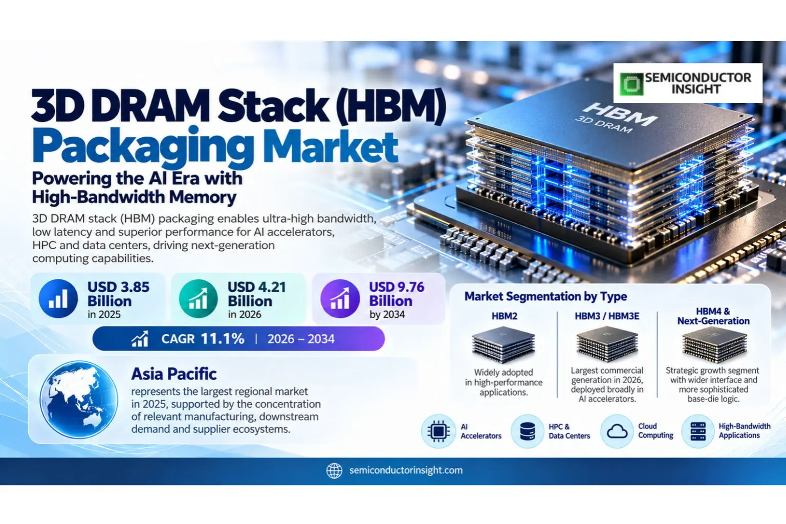
- 3d dram stack (hbm) packaging market was valued at USD 3.85 billion in 2025 and is projected to reach USD 9.76 billion by 2034, representing a 11.1% CAGR over 2026–2034.
- The market is valued at USD 3.85 billion in 2025 and is projected to reach USD 9.76 billion by 2034, representing an 11.1% CAGR over 2026–2034.
- HBM3/HBM3E remains the volume center in 2026, while HBM4 is shifting package design toward wider interfaces, more complex base dies and tighter logic-memory co-optimization.
- AI accelerators and data centers dominate demand because model training and inference require far more memory bandwidth than conventional server architectures can provide efficiently.
- Asia Pacific leads through South Korean HBM manufacturing and Taiwan’s advanced packaging ecosystem, while U.S. AI accelerator companies shape package specifications and capacity requirements.
3D DRAM Stack (HBM) Packaging Market Overview
3d dram stack (hbm) packaging market was valued at USD 3.85 billion in 2025, is estimated at USD 4.21 billion in 2026, and is projected to reach USD 9.76 billion by 2034, advancing at a 11.1% CAGR during 2026–2034. Asia Pacific represents the largest regional market in 2025, supported by the concentration of relevant manufacturing, downstream demand and supplier ecosystems.
3D DRAM stack packaging for high-bandwidth memory vertically integrates multiple DRAM dies over a logic or base die and connects them through through-silicon vias, fine interconnects and advanced package substrates. The architecture dramatically widens the memory interface and shortens electrical paths, enabling much higher bandwidth per watt than conventional DIMM-based memory for accelerator-class computing.
The packaging challenge is becoming more demanding with every HBM generation. HBM4 doubles interface width, increases total stack bandwidth and places greater emphasis on base-die integration, thermal control, warpage and known-good-die yield. Package suppliers therefore compete on stacking accuracy, underfill, interposer density, test strategy and the ability to co-design memory with logic packaging.
The commercial structure of the 3d dram stack (hbm) packaging market is shaped by design qualification, production economics and the interaction between component performance and downstream system requirements. Suppliers that can combine consistent manufacturing, application engineering and supply assurance are better positioned to convert technical eligibility into repeat business. Customer decisions increasingly account for lifecycle continuity, geographic resilience and integration cost, which makes proven process control and ecosystem compatibility as important as nominal product capability.
Segment Analysis: By Type
By type, the 3D DRAM Stack (HBM) Packaging market is segmented into HBM2, HBM3 / HBM3E, HBM4 & Next-Generation. HBM3 and HBM3E remain the largest commercial generation in 2026 because they are deployed broadly in AI accelerators already in volume production. HBM4 is the strategic growth segment, bringing a wider interface and more sophisticated base-die logic while increasing packaging complexity. Purchasing decisions vary by performance requirement, qualification burden, integration complexity and lifecycle economics, so suppliers compete on application fit rather than on a single technical specification.
| Type | Role in the market | Demand characteristics |
|---|---|---|
| HBM2 | HBM2 addresses a distinct part of the product and process mix. Its commercial position depends on technical fit, manufacturing maturity, integration requirements and customer qualification rather than on headline specifications alone. | Demand is strongest where the segment aligns with established customer designs, predictable supply, and measurable system-level performance. Suppliers that can document repeatability, compatibility and lifecycle support are better placed to defend design wins. |
| HBM3 / HBM3E | HBM3 / HBM3E addresses a distinct part of the product and process mix. Its commercial position depends on technical fit, manufacturing maturity, integration requirements and customer qualification rather than on headline specifications alone. | Demand is strongest where the segment aligns with established customer designs, predictable supply, and measurable system-level performance. Suppliers that can document repeatability, compatibility and lifecycle support are better placed to defend design wins. |
| HBM4 & Next-Generation | HBM4 & Next-Generation addresses a distinct part of the product and process mix. Its commercial position depends on technical fit, manufacturing maturity, integration requirements and customer qualification rather than on headline specifications alone. | Demand is strongest where the segment aligns with established customer designs, predictable supply, and measurable system-level performance. Suppliers that can document repeatability, compatibility and lifecycle support are better placed to defend design wins. |
Segment Analysis: By Stacking Technology
By stacking technology, the 3D DRAM Stack (HBM) Packaging market is segmented into TSV + Microbump, Hybrid Bonding, Advanced Molded Underfill. TSV plus microbump architectures remain mainstream, while advanced molded underfill improves warpage and thermal stability in tall stacks. Hybrid bonding is increasingly relevant as interconnect pitch shrinks and bump scaling becomes more difficult. Purchasing decisions vary by performance requirement, qualification burden, integration complexity and lifecycle economics, so suppliers compete on application fit rather than on a single technical specification.
| Stacking Technology | Role in the market | Demand characteristics |
|---|---|---|
| TSV + Microbump | TSV + Microbump represents a relevant purchasing and deployment pathway within this market. Commercial attractiveness depends on how well it aligns with customer architecture, supply-chain constraints and required performance. | Growth is linked to design-in activity, installed-base transitions and the ability of suppliers to meet qualification, cost and availability requirements over the full product lifecycle. |
| Hybrid Bonding | Hybrid Bonding represents a relevant purchasing and deployment pathway within this market. Commercial attractiveness depends on how well it aligns with customer architecture, supply-chain constraints and required performance. | Growth is linked to design-in activity, installed-base transitions and the ability of suppliers to meet qualification, cost and availability requirements over the full product lifecycle. |
| Advanced Molded Underfill | Advanced Molded Underfill represents a relevant purchasing and deployment pathway within this market. Commercial attractiveness depends on how well it aligns with customer architecture, supply-chain constraints and required performance. | Growth is linked to design-in activity, installed-base transitions and the ability of suppliers to meet qualification, cost and availability requirements over the full product lifecycle. |
Segment Analysis: By Application
By application, the 3D DRAM Stack (HBM) Packaging market is segmented into AI Accelerators & Data Centers, High-End Graphics, Supercomputing, Automotive & Edge Computing. AI accelerators and data centers account for most value because HBM directly addresses the bandwidth bottleneck in large-model training and inference. Supercomputing and high-end graphics remain important, while automotive and edge use cases are longer-term opportunities where cost and thermal constraints are stricter. Purchasing decisions vary by performance requirement, qualification burden, integration complexity and lifecycle economics, so suppliers compete on application fit rather than on a single technical specification.
| Application | Role in the market | Demand characteristics |
|---|---|---|
| AI Accelerators & Data Centers | AI Accelerators & Data Centers creates demand when the underlying system requires the market’s core function at production scale. Procurement is normally tied to platform launches, equipment upgrades, capacity expansion or replacement cycles. | Buyers evaluate reliability, qualification time, integration cost and vendor support alongside unit economics. Adoption accelerates when the solution removes a system bottleneck or supports a new performance tier without creating disproportionate redesign risk. |
| High-End Graphics | High-End Graphics creates demand when the underlying system requires the market’s core function at production scale. Procurement is normally tied to platform launches, equipment upgrades, capacity expansion or replacement cycles. | Buyers evaluate reliability, qualification time, integration cost and vendor support alongside unit economics. Adoption accelerates when the solution removes a system bottleneck or supports a new performance tier without creating disproportionate redesign risk. |
| Supercomputing | Supercomputing creates demand when the underlying system requires the market’s core function at production scale. Procurement is normally tied to platform launches, equipment upgrades, capacity expansion or replacement cycles. | Buyers evaluate reliability, qualification time, integration cost and vendor support alongside unit economics. Adoption accelerates when the solution removes a system bottleneck or supports a new performance tier without creating disproportionate redesign risk. |
| Automotive & Edge Computing | Automotive & Edge Computing creates demand when the underlying system requires the market’s core function at production scale. Procurement is normally tied to platform launches, equipment upgrades, capacity expansion or replacement cycles. | Buyers evaluate reliability, qualification time, integration cost and vendor support alongside unit economics. Adoption accelerates when the solution removes a system bottleneck or supports a new performance tier without creating disproportionate redesign risk. |
Segment Analysis: By Packaging Platform
By packaging platform, the 3D DRAM Stack (HBM) Packaging market is segmented into CoWoS / Interposer-Based, Fan-Out / RDL-Based, 3D Stack / SoIC-Class. Interposer-based platforms such as CoWoS dominate leading AI accelerators because they integrate logic and several HBM stacks at very high bandwidth. RDL and 3D stacking approaches expand the design space for larger and more heterogeneous systems. Purchasing decisions vary by performance requirement, qualification burden, integration complexity and lifecycle economics, so suppliers compete on application fit rather than on a single technical specification.
| Packaging Platform | Role in the market | Demand characteristics |
|---|---|---|
| CoWoS / Interposer-Based | CoWoS / Interposer-Based represents a relevant purchasing and deployment pathway within this market. Commercial attractiveness depends on how well it aligns with customer architecture, supply-chain constraints and required performance. | Growth is linked to design-in activity, installed-base transitions and the ability of suppliers to meet qualification, cost and availability requirements over the full product lifecycle. |
| Fan-Out / RDL-Based | Fan-Out / RDL-Based represents a relevant purchasing and deployment pathway within this market. Commercial attractiveness depends on how well it aligns with customer architecture, supply-chain constraints and required performance. | Growth is linked to design-in activity, installed-base transitions and the ability of suppliers to meet qualification, cost and availability requirements over the full product lifecycle. |
| 3D Stack / SoIC-Class | 3D Stack / SoIC-Class represents a relevant purchasing and deployment pathway within this market. Commercial attractiveness depends on how well it aligns with customer architecture, supply-chain constraints and required performance. | Growth is linked to design-in activity, installed-base transitions and the ability of suppliers to meet qualification, cost and availability requirements over the full product lifecycle. |
Regional Analysis
Asia Pacific leads the 3d dram stack (hbm) packaging market in 2025, while regional growth patterns differ according to manufacturing concentration, customer investment cycles, regulation, product mix and supply-chain access. The most important regional distinction is not simply market size; it is the mechanism that converts local investment and end-market demand into qualified purchases.
How does regional demand differ across the 3d dram stack (hbm) packaging market?
Regional demand for 3d dram stack (hbm) packaging is structurally uneven because manufacturing assets, design centers, downstream customers and qualification ecosystems are not distributed evenly. Asia Pacific typically has the deepest electronics manufacturing base, North America combines technology development with capital investment, Europe emphasizes reliability and industrial requirements, and emerging regions are more dependent on imported systems. These differences influence vendor selection, inventory policy, service expectations and the pace at which new technologies are adopted.
| Region | Market position | Growth outlook | Demand profile | Supplier-selection gate |
|---|---|---|---|---|
| Asia Pacific | Largest | Very strong | HBM manufacturing and advanced packaging led | Yield, packaging capacity and thermal control |
| North America | Largest demand center | Very strong | AI accelerator and cloud led | HBM allocation and package availability |
| Europe | High-value niche | Strong | HPC, automotive and research led | Access to leading packages |
| South America | Emerging | Moderate | Cloud and research led | AI infrastructure scale |
| Middle East & Africa | Developing | Strong from smaller base | Sovereign AI and data-center led | Accelerator supply and power availability |
Detailed Regional Blocks
Competitive Landscape
Competition in the 3d dram stack (hbm) packaging market is determined by technical qualification, manufacturing consistency, customer relationships and the ability to support product lifecycles. Price matters, but it rarely overrides reliability, integration effort or switching cost once a supplier has been designed into a production platform.
The competitive field includes SK hynix, Samsung Electronics, Micron Technology, TSMC, ASE Technology, Amkor Technology, alongside other specialized suppliers. Market share can shift when a vendor gains access to a new platform, expands qualified capacity or introduces a technology that materially improves system performance. Because customer validation can be lengthy, incumbent suppliers often benefit from continuity, while challengers need a clear technical or supply-chain advantage to displace an approved source.
Competitive strategy is increasingly multi-dimensional. Leading suppliers invest in process or product development, application engineering and regional support at the same time, while customers seek second-source options where technically feasible. This creates a market in which differentiation is sustained through documented performance, manufacturing yield, quality systems, responsiveness and the ability to support future roadmap transitions without forcing unnecessary redesigns.
| Company | Competitive position | Primary basis of competition |
|---|---|---|
| SK hynix | Established global / strategic supplier | Competes through product capability, qualification, account access and supply execution. |
| Samsung Electronics | Established global / strategic supplier | Competes through product capability, qualification, account access and supply execution. |
| Micron Technology | Established global / strategic supplier | Competes through product capability, qualification, account access and supply execution. |
| TSMC | Specialist / regional competitor | Competes through product capability, qualification, account access and supply execution. |
| ASE Technology | Specialist / regional competitor | Competes through product capability, qualification, account access and supply execution. |
| Amkor Technology | Specialist / regional competitor | Competes through product capability, qualification, account access and supply execution. |
| Powertech Technology | Focused challenger / niche participant | Competes through product capability, qualification, account access and supply execution. |
| NVIDIA | Focused challenger / niche participant | Competes through product capability, qualification, account access and supply execution. |
| AMD | Focused challenger / niche participant | Competes through product capability, qualification, account access and supply execution. |
Production Capacity Analysis
HBM packaging capacity is limited by TSV-enabled DRAM output, stacking equipment, underfill, base-die supply, interposer capacity and final package assembly. The bottleneck can shift among these stages as each generation introduces new process requirements.
South Korea leads memory-stack output while Taiwan leads advanced logic-memory integration. Capacity is expanding in both regions, and the announced U.S. HBM packaging build-out will add another strategic node later in the decade.
Capacity should therefore be evaluated on a qualified-output basis rather than as nominal installed capability. A supplier may possess equipment or production lines that appear suitable but still require customer-specific validation, process tuning, test correlation or upstream material qualification. This distinction becomes especially important during demand spikes, when headline capacity can overstate the volume that is immediately available for a particular application, technology generation or reliability class.
Market Dynamics
The 3d dram stack (hbm) packaging market is being shaped by rising performance requirements and technology transitions on the demand side, while qualification complexity, supply concentration and cost discipline constrain the pace of adoption. The balance of these forces favors suppliers that can solve a measurable system problem without increasing integration risk.
Demand expansion is not uniform across all product variants or customer groups. New technology creates attractive design opportunities, but buyers typically require a clear economic or performance case before changing a qualified architecture. At the same time, supply-chain localization, capacity investment and tighter quality requirements are changing procurement behavior. As a result, growth is likely to concentrate around applications where performance upgrades, manufacturing scale and lifecycle value reinforce one another.
Market Drivers
Four forces provide the strongest support for demand in the 3d dram stack (hbm) packaging market: performance-driven technology upgrades, expansion of relevant downstream applications, investment in manufacturing or infrastructure, and the need for more resilient supply. Their importance varies by segment, but each creates a direct reason for customers to qualify or purchase additional solutions.
| Driver | Impact | Commercial mechanism |
|---|---|---|
| AI models require extreme memory bandwidth | High | Training and inference workloads move large parameter and activation datasets, making HBM a core accelerator resource. |
| HBM4 increases bandwidth and interface width | High | The new generation expands package complexity and value through more I/O and advanced base-die integration. |
| CoWoS-class packaging is scaling rapidly | Medium-High | Larger interposers support more compute chiplets and HBM stacks in one package. |
| Energy efficiency matters in data centers | Medium-High | Short interconnects and wide interfaces reduce energy per bit compared with conventional off-package memory. |
AI models require extreme memory bandwidth
Training and inference workloads move large parameter and activation datasets, making HBM a core accelerator resource. The commercial effect is strongest where customers can link the technology change to higher throughput, lower power, improved reliability, reduced lifecycle cost or access to a new end-market requirement.
HBM4 increases bandwidth and interface width
The new generation expands package complexity and value through more I/O and advanced base-die integration. The commercial effect is strongest where customers can link the technology change to higher throughput, lower power, improved reliability, reduced lifecycle cost or access to a new end-market requirement.
CoWoS-class packaging is scaling rapidly
Larger interposers support more compute chiplets and HBM stacks in one package. The commercial effect is strongest where customers can link the technology change to higher throughput, lower power, improved reliability, reduced lifecycle cost or access to a new end-market requirement.
Energy efficiency matters in data centers
Short interconnects and wide interfaces reduce energy per bit compared with conventional off-package memory. The commercial effect is strongest where customers can link the technology change to higher throughput, lower power, improved reliability, reduced lifecycle cost or access to a new end-market requirement.
Market Restraints
Growth is moderated by qualification burden, cyclical purchasing, technology substitution and supply-chain risk. These restraints do not eliminate demand, but they can extend sales cycles, limit supplier switching and reduce the speed at which technically superior solutions convert into production revenue.
| Restraint | Impact | Commercial consequence |
|---|---|---|
| Packaging yield is difficult | High | Stacking many expensive DRAM dies means a single defect can reduce package yield materially. |
| Advanced packaging capacity is constrained | High | Interposers, TSV processing and high-precision assembly require specialized facilities. |
| Thermal density is rising | Medium | Tall HBM stacks next to high-power logic create difficult heat-removal challenges. |
| Capital intensity is high | Medium | HBM and CoWoS capacity expansion requires substantial investment in both memory fabs and packaging lines. |
Packaging yield is difficult
Stacking many expensive DRAM dies means a single defect can reduce package yield materially. Suppliers can mitigate part of this pressure through stronger qualification support, transparent lifecycle planning, dual-source strategies and better alignment between product roadmaps and customer production schedules.
Advanced packaging capacity is constrained
Interposers, TSV processing and high-precision assembly require specialized facilities. Suppliers can mitigate part of this pressure through stronger qualification support, transparent lifecycle planning, dual-source strategies and better alignment between product roadmaps and customer production schedules.
Thermal density is rising
Tall HBM stacks next to high-power logic create difficult heat-removal challenges. Suppliers can mitigate part of this pressure through stronger qualification support, transparent lifecycle planning, dual-source strategies and better alignment between product roadmaps and customer production schedules.
Capital intensity is high
HBM and CoWoS capacity expansion requires substantial investment in both memory fabs and packaging lines. Suppliers can mitigate part of this pressure through stronger qualification support, transparent lifecycle planning, dual-source strategies and better alignment between product roadmaps and customer production schedules.
Market Opportunities
The most attractive opportunities in the 3d dram stack (hbm) packaging market occur where a technology transition creates measurable value and where suppliers can enter before the customer architecture is locked. Early engagement, application-specific engineering and credible supply planning can convert these windows into durable design positions.
HBM4 and HBM4E
Wider interfaces and higher bandwidth create greater package value and tighter logic-memory co-design. The opportunity is strongest for suppliers that can demonstrate performance with production-relevant data, provide engineering support during qualification and maintain a roadmap that gives customers confidence in long-term availability.
Hybrid bonding
Finer-pitch direct bonding can reduce interconnect resistance and enable future stack scaling. The opportunity is strongest for suppliers that can demonstrate performance with production-relevant data, provide engineering support during qualification and maintain a roadmap that gives customers confidence in long-term availability.
U.S. advanced packaging localization
New HBM packaging capacity in Indiana broadens geographic supply resilience. The opportunity is strongest for suppliers that can demonstrate performance with production-relevant data, provide engineering support during qualification and maintain a roadmap that gives customers confidence in long-term availability.
Larger AI packages
More HBM stacks per accelerator package increase packaging content per system. The opportunity is strongest for suppliers that can demonstrate performance with production-relevant data, provide engineering support during qualification and maintain a roadmap that gives customers confidence in long-term availability.
Supply Chain Analysis
HBM DRAM die fabrication
Memory vendors manufacture tested DRAM dies and logic base dies. Value capture at this stage depends on quality consistency, technical differentiation and the difficulty of substitution. Bottlenecks can propagate downstream when qualification or material compatibility prevents customers from shifting quickly to an alternative supplier.
TSV stacking and underfill
Dies are vertically connected, stacked and mechanically stabilized. Value capture at this stage depends on quality consistency, technical differentiation and the difficulty of substitution. Bottlenecks can propagate downstream when qualification or material compatibility prevents customers from shifting quickly to an alternative supplier.
Interposer and advanced package integration
HBM stacks are placed next to accelerator dies on silicon or RDL-based package structures. Value capture at this stage depends on quality consistency, technical differentiation and the difficulty of substitution. Bottlenecks can propagate downstream when qualification or material compatibility prevents customers from shifting quickly to an alternative supplier.
System qualification
Packaged accelerators are tested for bandwidth, power, thermal behavior and long-duration reliability. Value capture at this stage depends on quality consistency, technical differentiation and the difficulty of substitution. Bottlenecks can propagate downstream when qualification or material compatibility prevents customers from shifting quickly to an alternative supplier.
Recent Developments
Recent developments show how technology roadmaps, manufacturing investment and standards are changing the competitive requirements of the 3d dram stack (hbm) packaging market. The entries below are selected for their direct relevance to product capability, capacity, qualification or downstream adoption rather than for general corporate activity.
Samsung began commercial shipment of HBM4 with an industry-first 2048-bit interface, 11.7 Gbps operation and a 4nm logic base die, marking the transition to a more complex sixth-generation HBM package. Source
SK hynix reported that HBM4 mass shipments had begun in the second quarter and that it was accelerating advanced-packaging capacity expansion to address structural AI-memory demand. Source
TSMC’s 3DFabric roadmap continues to expand CoWoS-L and SoIC integration for AI/HPC, including package structures designed to combine logic with multiple HBM stacks. Source
Report Scope & Segmentation
| Report attribute | Coverage |
|---|---|
| Market | 3D DRAM Stack (HBM) Packaging |
| Base Year | 2025 |
| Estimated Year | 2026 |
| Forecast Period | 2026–2034 |
| 2025 Market Size | USD 3.85 billion |
| 2026 Estimated Size | USD 4.21 billion |
| 2034 Forecast Size | USD 9.76 billion |
| CAGR (2026–2034) | 11.1% |
| Largest Market in 2025 | Asia Pacific |
| By Type | HBM2, HBM3 / HBM3E, HBM4 & Next-Generation |
| By Application | AI Accelerators & Data Centers, High-End Graphics, Supercomputing, Automotive & Edge Computing |
| By Stacking Technology | TSV + Microbump, Hybrid Bonding, Advanced Molded Underfill |
| By Packaging Platform | CoWoS / Interposer-Based, Fan-Out / RDL-Based, 3D Stack / SoIC-Class |
| Companies Profiled | SK hynix, Samsung Electronics, Micron Technology, TSMC, ASE Technology, Amkor Technology, Powertech Technology, NVIDIA, AMD |
Frequently Asked Questions
What was the 3d dram stack (hbm) packaging market size in 2025?
The global 3d dram stack (hbm) packaging market was valued at USD 3.85 billion in 2025. The 2025 value is the base-year reference used throughout this overview and provides the starting point for comparing the 2026 estimate and the 2034 forecast.
What is the projected 3d dram stack (hbm) packaging market size in 2034?
The global market is projected to reach USD 9.76 billion by 2034. The forecast reflects the interaction of downstream adoption, technology transitions, production investment and the qualification requirements that shape commercial conversion across the market.
What is the CAGR of the 3d dram stack (hbm) packaging market from 2026 to 2034?
The 3d dram stack (hbm) packaging market is expected to expand at a 11.1% CAGR during 2026–2034. Growth will not be uniform across every product or region because customer qualification, capital cycles, supply constraints and application-specific performance requirements differ materially.
Which region is the largest 3d dram stack (hbm) packaging market?
Asia Pacific is the largest regional market in 2025. Its position is supported by the concentration of relevant manufacturing, customers, technology ecosystems and downstream demand, although the precise commercial mechanism differs by country and application.
How is the 3d dram stack (hbm) packaging market segmented by type?
By type, the market is segmented into HBM2, HBM3 / HBM3E, HBM4 & Next-Generation. These categories address different performance, cost and integration requirements, so supplier selection depends on application fit, qualification history and lifecycle economics rather than a single specification.
What are the main applications for 3d dram stack (hbm) packaging?
By application, the market covers AI Accelerators & Data Centers, High-End Graphics, Supercomputing, Automotive & Edge Computing. Demand in each application is linked to platform launches, capacity expansion, equipment replacement and the degree to which the technology improves system performance or manufacturing economics.
What are the principal growth drivers for the 3d dram stack (hbm) packaging market?
Key drivers include ai models require extreme memory bandwidth and hbm4 increases bandwidth and interface width. These forces increase demand when customers can translate technical improvements into higher performance, lower cost, greater reliability or access to new applications.
What are the main restraints in the 3d dram stack (hbm) packaging market?
Important restraints include packaging yield is difficult and advanced packaging capacity is constrained. The resulting qualification burden, purchasing cyclicality and technology risk can extend sales cycles and limit rapid supplier substitution even when new solutions offer clear technical advantages.
Which companies participate in the 3d dram stack (hbm) packaging market?
Companies profiled in this market include SK hynix, Samsung Electronics, Micron Technology, TSMC, ASE Technology, Amkor Technology, Powertech Technology, NVIDIA. Competition centers on qualification, product or process performance, manufacturing consistency, customer support and the ability to maintain supply across the required product lifecycle.
What should buyers evaluate when selecting a 3d dram stack (hbm) packaging supplier?
Buyers should evaluate demonstrated performance, qualification history, manufacturing consistency, lifecycle support, supply resilience and integration cost. A technically strong product can still face adoption barriers if it increases redesign risk, lacks regional support or cannot meet the customer’s production and quality requirements.
Research Sources & Evidence Base
View research sources used for this overview.
- Samsung Electronics. HBM4 commercial shipment — HBM4 interface, speed, logic base die and mass-production details.
- SK hynix. 2Q26 Financial Results — HBM4 mass shipment and advanced-packaging capacity expansion context.
- TSMC. 2025 Annual Report — CoWoS, SoIC and HBM-integrated advanced-packaging roadmap.
- SK hynix. HBM4 / TSMC collaboration — HBM4 base-die and packaging co-development context.
Get Sample Report PDF for Exclusive Insights
Report Sample Includes
- Table of Contents
- List of Tables & Figures
- Charts, Research Methodology, and more...
 Download Sample Report PDF


