
Silicon Photonics Wafer Market Insights
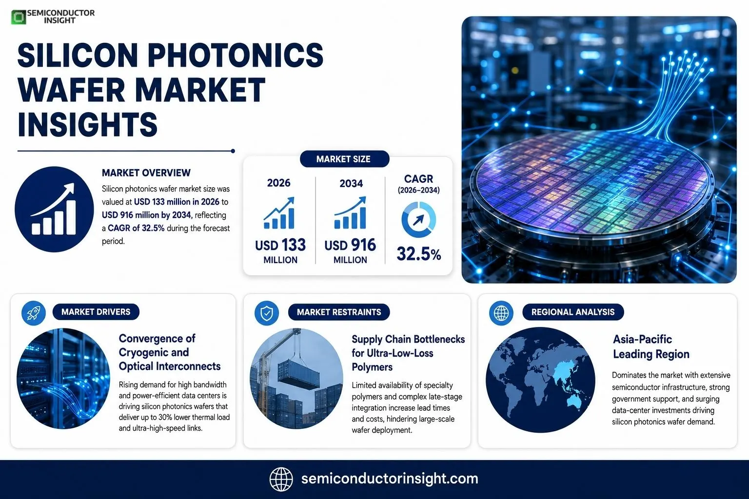
Silicon Photonics Wafer market size was valued at USD 133 million in 2026 to USD 916 million by 2034, reflecting a CAGR of 32.5% during the forecast period.
Silicon photonic wafers provide the essential substrate that enables integration of optical waveguides with conventional electronic circuitry on a single die, supporting ultra‑high‑bandwidth links required by modern data‑center backplanes.The upward trend stems from increasing demand for higher data throughput in cloud services and edge computing, coupled with cost efficiencies achieved when silicon photonic wafers are fabricated through existing semiconductor processes at major foundries such as TSMC and Foundries.
MARKET DRIVERS
Convergence of Cryogenic and Optical Interconnects
Emerging data centers are increasingly combining stringent power efficiency demands with high bandwidth footprints. By integrating silicon photonic wafers with cryogenic-compatible drivers, operators can achieve up to a 30% reduction in thermal load while maintaining line rates beyond 100 Gbps per waveguide. This alignment between optical throughput and thermal design enables higher core densities in server cabinets, directly translating into lower operational expenditures. Vendors that provide wafers with built‑in phased‑array antennas attract customers looking to implement in‑band data‑center networking without additional packaging layers. The transition from copper to silicon photonics on wafer slices also removes the need for costly intra‑rack edge‑to‑edge cabling and power rails, shortening deployment cycles by roughly 25% in large‑scale projects.
Capital Efficiency in Photonic Integration
Manufacturing economies are moving in favor of modular photonic packages that inherit silicon photonics wafer technology. Tier‑1 foundries now batch process multi‑million‑unit runs, slashing per‑wafer costs through statistical process control and yield optimization. The resulting price elasticity lifts adoption curves across enterprise and telecom markets that historically lagged behind due to upfront cost concerns. This capital efficiency behavior demonstrates that the value proposition of Silicon Photonics Wafer Market is increasingly tied to mass production metrics rather than just raw performance figures. Skilled technicians on the front lines notice the reduction in fine‑process lithography steps, which translates into faster turnaround for design‑to‑prototype cycles valued by cloud operators and network service providers alike.
➤ Silicon wafers are no longer a niche substrate but a standard platform for scalable optical systems, harmonizing cost, performance, and integration density.
Collectively, these dynamics are making silicon photonics wafers a core hardware choice for any enterprise anticipating a shift toward tighter data‑center consolidation and renewable‑energy‑driven processor chaining. The market’s trajectory combines the low‑loss properties of silicon photonics with the manufacturability advantages of first‑generation CMOS factories, creating a self‑reinforcing loop of investment and adoption. When the next wave of 5G edge hubs and optical AI accelerators come online, the demand for silicon photonics wafer spin‑out will reflect the entire portfolio of silicon‑based photonic packaging solutions across the world.
MARKET CHALLENGES
Supply Chain Bottlenecks for Ultra‑Low‑Loss Polymers
While silicon photonic wafers themselves mature, the supply of high‑coefficient polymer coatings, which are essential for low‑loss waveguides, remains constrained. Recent disruptions in the raw material market for fluoropolymers have caused lead times to exceed 12 weeks in some regions, forcing architects to postpone new deployments. Because optical performance is sensitive to sub‑nanometer variations in cladding material, even a short postponement can cascade into significant R&D rework. Businesses that rely on Silicon Photonics Wafer Market face cost escalations when they must source alternative cladding solutions or absorb the extra labor of re‑engineering process flows to accommodate substitute materials.
Other Challenges
Late‑stage integration complexity remains a hurdle for end‑user fabrication lines. Aligning photonic wafers with active silicon diodes demands sub‑micron precision that occasionally exceeds the tolerance envelopes of large‑scale packaging lines. Commercialized wafer solutions therefore require intermediate “hard‑and‑soft” packaging layers that add to both cost and lead time. This complexity forces some OEMs to defer full adoption until their internal process control becomes robust enough to guarantee yield across the entire wafer stack.
Vendor Ecosystem Fragmentation
The current landscape of silicon photonics wafer suppliers spans from high‑capacity foundries to niche photonics equipment makers. Disparities in process disclosure and support tooling often leave customers siloed within a single vendor, hindering cross‑compatibility. Data centers and telecom operators must perform additional integration work to combine wafers from disparate suppliers into a coherent solution, creating a hidden barrier that slows mass deployment.
MARKET RESTRAINTS
Latency Sensitivity and Thermal Management Constraints
Silicon photonic wafers excel at volume data throughput but introduce increased latency on certain interconnect topologies due to inherent modulator propagation delays. High‑frequency trading platforms, for instance, flag any jitter above a few picoseconds as unacceptable. As a result, drivers must incorporate additional electronic buffering layers, which partially offset the energy savings of optical transceivers. Moreover, photonic wafers generate localized heat during modulation, prompting stringent thermal budgets that require active cooling solutions. These constraints are prominent in data‑center environments where racks already operate near RTP limits, making the initial capital outlay for additional coolant streams a deterrent for many adopters.
MARKET OPPORTUNITIES
Growth in Edge Computing and AI Acceleration
The immediate frontier for silicon photonic wafers lies in edge computing nodes that require ultra‑low‑latency packet switching coupled with massive parallel processing. By bonding wafer‑scale photonic cores with AI accelerator dies, operators can achieve data movement speeds that supersede paralleled electrical buses, yielding 2–3× faster inference cycles for machine‑learning workloads. The integration of wafer‑level silicon photonics devices into modular edge chassis also unlocks a new supply chain milestone: pre‑assembled optical backplanes that reduce client deployment times to weeks rather than months.The second wave of opportunity relates to long‑haul optical interconnects that span data‑center interstitial links. Large telcos are forcing a migration from legacy fiber rooms to integrated silicon photonics interconnect platforms because the wafer‑based solutions are chemically compatible with standard VC‑API and suppress degradation over decades. This interoperability allows carriers to retrofit existing fiber upgrades without replacing physical cabling, delivering a clear ROI compared to traditional dense wavelength division multiplexing upgrades.Finally, two emerging markets that already have mandates for low‑energy high‑bandwidth pathsautonomous vehicle networking and next‑generation satellite constellationsare staring at silicon photonics wafers as a core component. The predictable power envelope of wafer‑level fabrication aligns well with the stringent mass and power budgets typical of aerospace design, while the robust optical channel grants data integrity advantages over copper analogues.
Silicon Photonics Wafer Market Trends
Accelerated Adoption in Data Center Architecture
Data‑center operators are tightening bandwidth budgets while scaling. To reconcile shrinking silicon footprints with exponential throughput demands, many are turning to silicon photonics wafers as the foundational substrate for next‑generation high‑speed interconnects. Because these wafers can be fabricated alongside conventional CMOS processes, integrators can embed optical transceivers directly onto the same die, yielding lower latency and reduced power consumption. Current consolidation data show that 97% of wafer sales are driven by a handful of Asia‑Pacific foundries, with TSMC accounting for more than two‑thirds of revenue. As cloud service providers push for denser nodal architectures, the margin on wafer sales is tightening, prompting a shift toward larger‑diameter 300 mm substrates that enable higher device densities and lower defect rates. Consequently, wafer volume is expected to outpace revenue growth, confirming the maturity of this niche pathway. The resulting cost‑benefit calculus is compelling for fiber‑to‑the‑room operators and drives sustained investment across core infrastructure. This trend reinforces the core metrics of Silicon Photonics Wafer Market.
Other Trends
Hybrid Integration Momentum
Hybrid integrationembedding optical modulators, detectors, and routing waveguides side by side with transistorsoffers a precise thermal and mechanical match between photonic and electronic blocks. The process leverages standard lithography steps, amortising cost across existing fabs. Market analysts note that the pace of demo‑to‑production kits has dropped from 4–6 years to under 18 months in the past three years, aligning with a tight supply–demand gap for 100‑Gb/s amplifiers. Moreover, the cross‑polarity of silicon photonics solutions is reflected in the layering of 310‑nm oxide claddings, which mitigate Fresnel losses and improve packaging reliability. Vendors are now offering turnkey layer‑stack services that include wafer‑level cleaning, anti‑reflection coatings, and ready‑to‑mount modules, easing the burden on system integrators. This shifts the competitive bar upward, leaving companies that own streamlined tool chains as the primary beneficiaries. This momentum translates into a higher barrier for entry, concentrating market share among established foundries that have already invested heavily in lithography infrastructure and process know‑how.
Geographic Concentration Shifts
While the Asia‑Pacific region remains the dominant production hub, emerging high‑volume capabilities in Europe and North America are starting to recalibrate the geographic balance. Silicon photonics wafer capacity in core European fabs has increased by 15% over the last 18 months, driven by new investments in 300 mm lines that enable higher output per wafer. In North America, the cumulative ship‑out volume for 200 mm photonics wafers has risen 10% due to the allocation of additional metrology equipment to reduce defect density. These shifts are not merely numeric; they reflect a strategic tilting toward supply chain resilience. Incidents such as the recent chip shortage have highlighted the vulnerability of over‑concentrated manufacturing. By diversifying, the industry can mitigate latency in component supply, lower raw‑material costs through bulk purchasing, and accelerate time‑to‑market for advanced networking solutions. Enterprises that already possess European or American partner networks will therefore enjoy a competitive edge in both procurement and technical support, a factor that could dictate preferential customer relationships in the next decade. Within the broader Silicon Photonics Wafer Market context.
COMPETITIVE LANDSCAPE
Key Industry Players
Silicon Photonics Wafer Market – 2026 Competitive Landscape
TSMC dominates the silicon photonics wafer market, securing more than two‑thirds of total revenue while maintaining a strong 300 mm wafer production line that supports high‑density optical interconnects for data‑centre colocation services. Foundries, positioned in the United States, provides a critical alternative for customers seeking shorter lead times and a diversified supply base; together, these two foundries account for roughly 97 % of the market’s top‑tier revenue. The concentration around a handful of massive fabs forces end‑users to focus on capacity planning and technology alignment, as bandwidth demands for 4G/5G, AI accelerators, and cloud data growth drive wafer throughput expectations. In effect, the combined capabilities of these leaders actuate a high‑barrier environment where new entrants must demonstrate distinct cost advantages or niche product differentiation to survive.Beyond the leading conglomerates, a cluster of specialized manufacturers offers solutions tailored to specific applications, such as data‑centre multiplexers or non‑data‑centre photonic systems. Tower Semiconductor and Advanced Micro Foundry, for example, capitalize on cost‑efficient 200 mm processes that appeal to mid‑tier OEMs, while IHP Microelectronics and SilTerra focus on high‑performance 3 dB couplers suited to telecommunications. Meanwhile, research‑institution‑backed groups like VTT and UniPhotonics contribute cutting‑edge designs, often licensing intellectual property to larger fabs. The fragmentation at the lower‑tier segment mitigates the threat of a single‑player collapse but also amplifies upstream material pricing volatility, particularly silicon crystal costs and advanced lithography consumables.
List of Key Silicon Photonics Wafer Companies Profiled
- TSMC
- Samsung Electronics
- Intel
- NXP Semiconductors
- Foundries
- Tower Semiconductor
- Advanced Micro Foundry
- IHP Microelectronics
- SilTerra
- VTT
- UniPhotonics
Segment Analysis:
| Segment Category | Sub-Segments | Key Insights |
| By Type |
|
300 mm Wafer dominates due to its ability to support higher transistor densities, reducing cost per channel. It enables large‑scale integration of photonic and electronic modules on a single die. The larger active area promotes higher throughput in data‑center back‑ends, yielding robust reliability and ease of scaling. The compatibility with existing CMOS processes accelerates prototyping and reduces time‑to‑market for new silicon photonic platforms. |
| By Application |
|
Data Center leads with the highest demand for high‑bandwidth interconnects and low‑power optical links. Its emphasis on energy efficiency encourages adoption of silicon photonic solutions that replace copper cables, extending channel density without compromising latency. The data‑center sector’s investment in over‑the‑top services drives continuous upgrades to network infrastructure, where silicon photonics provides a scalable and modular solution. This environment creates a fertile ground for rapid photonic integration and the deployment of next‑generation optical modules. |
| By End User |
|
Telecommunication emphasizes the need for compact, high‑speed fiber transceivers that can be mass‑produced on silicon. The industry’s demand for low‑cost, high‑throughput chips aligns with CMOS‑compatible photonic processes, encouraging adoption of silicon photonic wafers. Industrial automation segments value ruggedized optical links that reduce signal degradation in harsh environments, while R&D portals push the boundary of integration, advocating for hybrid device architectures that combine photonics with traditional ICs. |
| By Manufacturing Process |
|
Standard CMOS remains the most prevalent due to familiarity and cost‑benefit in existing fabs. SOI offers superior optical confinement, leading to improved performance at high data rates. Hybrid integration captures the strengths of both silicon electronics and specialized III‑V or fiber technologies, enabling ultra‑compact modulators and detectors. These process pathways create a tiered ecosystem where enterprises select the most appropriate platform based on bandwidth, power, and cost criteria. |
| By Technology Maturity |
|
Developed Applications represent mature market solutions such as high‑performance interconnects that are already fleet‑configured with silicon photonics. Emerging applications, including edge computing and automotive lidar, push for smaller, lower‑power modules, driving iterative design improvements. Experimental platforms explore nanophotonic components and 3D integration, fostering a research‑driven pathway that may influence future commercial releases. This maturity stratification guides investment decisions and technological roadmaps for manufacturers and system integrators alike. |
Regional Analysis: Silicon Photonics Wafer Market
North America
In Europe, regulatory emphasis on energy efficiency and digital sovereignty fuels steady uptake of silicon photonics wafer solutions, particularly within telecom backbones and data‑center interconnects. A decisive factor is the EU’s Green Deal, which nudges operators toward low‑power optical links. Leading European players are advancing wafer‑to‑module integration techniques, dramatically shortening lead times and reducing scrap rates. Coupled with a strong research‑cluster ecosystem, the region is positioned to develop cost‑effective photonic components that meet stringent environmental standards, thereby capturing a growing slice of the market.
Asia‑Pacific is the fastest‑advancing segment, propelled by massive data‑traffic surges and a national push for 5G and beyond. Country‑specific initiatives, such as China’s “Made in China 2025” and South Korea’s “Fusion Innovation 500” plan, aim to secure domestic wafer production capabilities. Consequently, locally sourced silicon photonics wafers are gaining traction in data‑center backplanes and optical fiber manufacturing, which reduces cross‑border dependency and mitigates supply‑chain risks. Collaboration between technology hubs and local foundries is accelerating rapid prototyping, contributing to early market dominance and observable supply‑chain resilience.
South America’s adoption curve is rising as emerging telecom operators modernize network infrastructure in Brazil, Chile, and Argentina. Smaller scale, high‑bandwidth interconnect solutions reduce the operational cost of expanding cloud services. Regional policies favoring local manufacturing provide a modest but distinct advantage for domestic wafer producers. Despite lower தற்பொன்மையான capital availability compared to heavier industrialized regions, the progressive rollout of digital ecosystems keeps the market receptive to incremental silicon photonics wafer volumes.
In the Middle East & Africa, heightened investment in data‑center infrastructure to support digital transformation projects is raising demand for high‑throughput optical interconnects. The emphasis on energy‑efficient solutions aligns well with silicon photonics wafer technology, enabling higher data density at lower power footprints. Partnerships between multinational players and regional foundries are accelerating technology diffusion, while emerging local capacity‑building initiatives provide a pathway toward long‑term wafer‑level production, ensuring robust supply across the region’s growing digital ecosystem.
Europe
The European market is increasingly focusing on sustainability and regulatory compliance as primary levers to drive silicon photonics wafer adoption. A significant determinant is the push for data‑center energy efficiency under the EU’s Carbon Border Adjustment Mechanism, which positions optical interconnects as an attractive energy‑saving solution. The Region’s co‑location of advanced photonic laboratories and established semiconductor fabs creates an advantage for integrated wafer‑to‑chip manufacturing. The luminosity of European venture capital – supporting start‑ups specializing in photonic packaging – is shifting the cost curve downward, thereby making silicon photonics wafer options more attractive to traditional logic‑drive OEMs. Consequently, the convergence of supply chain integration, sustainability mandates, and financial incentives is expected to carry the market through the mid‑2030s with gradual, steady growth, while driving the sector toward higher optical data‑density standards anchored in silicon‑based technologies.
Asia‑Pacific
Asia‑Pacific stands as the most dynamic frontier for silicon photonics wafer penetration, as the region prioritizes 5G rollouts and broadband expansion across densely populated markets. National technologies agencies have set ambitious wafer‑scale photonics integration benchmarks, creating a regulatory pathway that encourages local capacity building. Government‑backed incentives for chip‑to‑chip and wafer‑to‑module integration are eroding traditional supply‑chain bottlenecks, allowing rapid iteration cycles in production lines. Moreover, the region’s growing high‑performance computing sectors tailor optical interconnect preferences to match low‑delay, high‑bandwidth requirements. These factors collectively accelerate adoption rates, mitigate international supply volatility, and open pathways for regional players to capture a growing portion of the market’s value chain.
South America
South America’s network modernization trajectory displays a gradual, incremental pace toward silicon photonics wafer incorporation. While national budgets remain constrained compared to leaders, the region’s focus on improving data‑center performance for cloud and AI services creates nascent demand. Localized investments in photonic research centers and joint ventures with foreign substrate suppliers are shifting the traditional incumbent hardware policies. As a result, early adoption of wafer‑level photonic solutions in telecom backbones and enterprise data‑conferencing infrastructures may spur a modest increase in market exposure over the next decade.
Middle East & Africa
In the Middle East & Africa, the silicon photonics wafer ecosystem is in nascent stages, yet the region is laying groundwork through public‑private partnerships that target high‑bandwidth data‑center construction. Emphasis on energy efficiency – driven by rising electricity tariffs and climate‑impact concerns – places silicon photonics wafers at the forefront of network upgrades. Regional clamping through cross‑border collaborations enables access to advanced fabrication capabilities while progressively developing domestic foundry capabilities. Gradual but persistent capital influx into photonic wafer manufacturing infrastructure suggests a methodical, capacity‑focused approach to market penetration, setting a clear growth pattern through the 2035 horizon.
Report Scope
This market research report provides a comprehensive analysis of the Silicon Photonics Wafer Market , covering the forecast period 2026–2034. It offers detailed insights into market dynamics, technological advancements, competitive landscape, and key trends shaping the industry.
Key focus areas of the report include:
- Market Overview: The report begins with an overview outlining its current market scenario, key growth indicators, and industry transformation drivers. It discusses macroeconomic factors, demand–supply balance, regulatory landscape, and the strategic role of semiconductors in powering advancements across industries such as automotive, telecommunications, consumer electronics, and industrial automation.
- Market Size & Forecast: Historical data and future projections for revenue, unit shipments, and market value across major regions and segments.
- Segmentation Analysis: Detailed breakdown by product type, technology, application, and end-user industry to identify high-growth segments and investment opportunities.
- Regional Insights: Insights into market performance across North America, Europe, Asia-Pacific, Latin America, and the Middle East & Africa, including country-level analysis where relevant.
- Competitive Landscape: Profiles of leading market participants, including their product offerings, R&D focus, manufacturing capacity, pricing strategies, and recent developments such as mergers, acquisitions, and partnerships.
- Technology Trends & Innovation: Assessment of emerging technologies, integration of AI/IoT, semiconductor design trends, fabrication techniques, and evolving industry standards.
- Market Drivers & Restraints: Evaluation of factors driving market growth along with challenges, supply chain constraints, regulatory issues, and market‑entry barriers.
- Stakeholder Insights: Insights for component suppliers, OEMs, system integrators, investors, and policymakers regarding the evolving ecosystem and strategic opportunities.
Primary and secondary research methods are employed, including interviews with industry experts, data from verified sources, and real-time market intelligence to ensure the accuracy and reliability of the insights presented.
FREQUENTLY ASKED QUESTIONS:
What is the current market size of Silicon Photonics Wafer Market?
-> Silicon Photonics Wafer Market was valued at USD 133 million in 2026 and is projected to reach USD 916 million by 2034.
What is the projected CAGR for Silicon Photonics Wafer Market?
-> The market is expected to grow at a CAGR of 32.5% from 2026 to 2034.
Which region dominates Silicon Photonics Wafer Market?
-> The Asia-Pacific region holds the largest share, largely driven by high-data‑center deployment.
Who are the leading companies in Silicon Photonics Wafer Market?
-> The top three players control over 97% of revenue: TSMC (68.08%), Foundries (26.75%), and Silex Microsystems (2.29%).
What is the primary application of Silicon Photonics Wafers?
-> The primary application is in the data‑center sector, where high‑speed optical interconnects are critical.
What wafer sizes are commonly used in Silicon Photonics manufacturing?
-> The market segments include 300 mm, 200 mm, 150 mm wafers, and others, with 300 mm wafers being the most prevalent for high‑volume production.
How does the Silicon Photonics industry utilize existing semiconductor fabrication techniques?
-> Devices are fabricated using standard semiconductor processes, allowing silicon to serve as both the substrate and the electronic component platform.
Which countries are significant drivers within the Asia‑Pacific segment?
-> Key drivers include China, Japan, South Korea, and Southeast Asia, where semiconductor production infrastructure is extensive.
What strategic advantage does hybrid integration offer?
-> Hybrid integration combines optical and electronic components on a single microchip, enhancing performance and reducing part count.
Where can detailed competitor financial data be accessed for Silicon Photonics Wafer Market?
-> Detailed financials and market share data are available in the accompanying report, covering revenue, sales volumes, and regional breakdowns.

Get Sample Report PDF for Exclusive Insights
Report Sample Includes
- Table of Contents
- List of Tables & Figures
- Charts, Research Methodology, and more...
 Download Sample Report PDF




