Wafer Thinning Services Market Insights
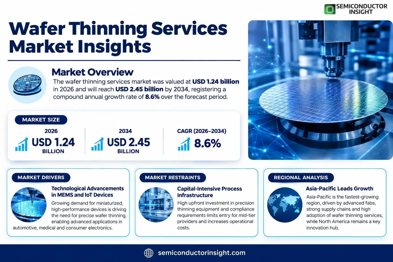
Wafer thinning services market was valued at USD 1.24 billion in 2026 and will reach USD 2.45 billion by 2034, registering a compound annual growth rate of 8.6% over the forecast period.
Wafer thinning services encompass precision mechanical grinding, chemical–mechanical planarisation (CMP) and selective etching that reduce silicon substrate thickness from the standard 775 µm down to sub‑50‑µm levels, enabling dense interconnects for advanced packaging solutions.This service stream underpins high‑performance technologies such as system‑in‑package (SiP), heterogeneous integration and high‑speed computing; thinner wafers improve signal integrity, lower parasitic capacitance and enhance thermal management across the semiconductor supply chain.
MARKET DRIVERS
Technological Advancements in MEMS and IoT Devices
The push toward finer feature sizes in mechanical-electrical-integrated systems has positioned wafer thinning as a critical step in producing compliant, high-performance MEMS solutions. Manufacturers prioritizing flexible circuitry and enhanced sensor resolution now turn to services that can spin wafers down to the 10–50 µm regime while preserving crystal integrity. This precision translates into lower power consumption and expanded application footprints, compelling device makers across automotive, medical diagnostics, and consumer electronics to adopt tailored thinning strategies. As a result, the wafer thinning services ecosystem is responding with an expanded suite of cryogenic dry lapping and ion beam polishing techniques that have been validated in recent release cycles, directly influencing component reliability metrics and reducing defect rates in high-density array packaging.
Rising Demand for Miniaturized Display Solutions
Ultra-thin substrates are becoming the backbone of flexible OLED and micro-LED display stacks, pushing the industry toward mass deployment of downscaled, roll‑to‑roll graphic panels. The advent of under‑display camera (UDC) modules and high‑resolution sensor arrays that necessitate sub‑10 µm dielectric layers can only be achieved through iterative thinning workflows that preserve planarity and surface roughness. The growing penetration of foldable smartphones and fold‑able tablets in emerging markets demands scalable wafer‐level thinning solutions that balance throughput with minimal thermal impact. End‑to‑end process integration now rewards firms that embed proprietary cleaning and defect mapping algorithms capable of operating on these ultra‑thin substrates, creating a clear technology advantage for companies that master these nuances.
➤ In the context of Wafer Thinning Services Market, demand is powered by a dual incentive: the relentless quest for device miniaturisation and the need for versatile substrates supporting advanced display solutions.
Strategically, partners can leverage economies of scale by collaborating with tier‑one silicon fabs to co‑develop custom thinning recipes. The adoption of AI‑driven process controls further assures optimal cycle times while keeping yields high, thereby reducing operating costs. Combined, these trends cement wafer thinning as a fundamental enabler for next‑generation electronics that look to maximize density without compromising performance.
MARKET CHALLENGES
Capital‑Intensive Process Infrastructure
While technical breakthroughs continue, the high capital outlay required for state‑of‑the‑art thinning equipmentcomprising ultra‑precise CMP systems and beam‑mediated polishing unitsremains a significant hurdle, limiting entry for mid‑tier providers. Equipment lifespan, typically 7‑10 years, forces operators to forecast demand accurately; misaligned projections can lead to underutilisation and skewed cost structures across the supply chain. Moreover, regulatory constraints surrounding the use of hazardous chemicals necessitate rigorous compliance protocols, which amplify upfront and ongoing expenditure for operators situated in regions with stringent environmental mandates. The increasing complexity of cleanroom classification to accommodate fine‑feature lithography also compounds operational budgets, dampening agility in responding to market fluctuations.
Other Challenges
Integration Bottlenecks with Advanced Packaging
Despite the promise of wafer‑level thinning, synchronising these services seamlessly with advanced package techniques such as 3‑D IC stacking and through‑silicon vias presents integration friction that continues to elevate risk profiles for end customers seeking streamlined supply chains.
MARKET RESTRAINTS
Limited Standardisation Across Regional Practices
Consistency in wafer thickness specifications remains fragmented across geographic markets, with differing tolerance windows reported in North America versus Asia. The absence of a unified standard hampers cross‑border collaboration, as manufacturers must repeatedly adapt process parameters to satisfy the target region’s compliance coding. This heterogeneity not only introduces quality variabilities but also heightens the risk of misaligned product performance that can erode brand equity in highly competitive segments.
Fluctuating Silicon Supply Chain Dynamics
Volatility in raw silicon availability due to geopolitical tensions and natural disasters has at times forced firms to adjust thinning batch sizes to accommodate real‑time inventory levels. These supply‑chain disruptions influence pricing structures, as thinner wafers necessitate more precise handling protocols that may become cost‐prohibitive. Consequently, the segment must navigate an environment where material unpredictability directly impacts throughput schedules and revenue timelines.
MARKET OPPORTUNITIES
Strategic Partnerships with Flexible Electronic Innovators
The shift toward flexible, bendable electronic skins for wearables and industrial sensors offers under‑exploited avenues for service firms. By establishing joint‑development agreements with primary display and sensor manufacturers, providers can embed proprietary thinning expertise directly into product design cycles. This collaborative model unlocks added‑value lanes that reduce time to market for clients and create recurring revenue streams for service operators through contractual maintenance packages and real‑time defect‑monitoring telematics. In parallel, emerging markets in Southeast Asia and Latin America demonstrate an uptake in wearable healthcare devices, presenting a high‑potential canvas for wafer‑level thinning solutions that can adapt to varying environmental constraints and temperature extremes.Targeted investments in automated defect‑inspection systems further enhance capacity to deliver high‑yield thin wafers, an attribute increasingly favoured by companies aiming to minimise recalls in medical implant devices. By capitalising on these ecosystem‑level incentives, service providers can anchor themselves as indispensable partners to a broader portfolio of consumer electronics and industrial automation players, cementing a competitive edge within the evolving Wafer Thinning Services Market.
Wafer Thinning Services Market Trends
Shift Toward Fine‑Grained Thinning and Low‑Stress CMP
Manufacturers increasingly favour ultra‑thin (30–60 µm) wafers to accommodate densely packed logic devices while mitigating device stress during flip‑chip bonding. This preference aligns with the broader industry push toward 300 mm silicon, which houses more transistors per wafer. Mechanical grinding continues to dominate, yet the proportion of chemical‑mechanical planarization (CMP) is rising steadily, reflecting a desire for smoother surfaces and tighter thickness tolerances. The resulting trend underscores a maturation of Wafer Thinning Services Market, where precision is now a competitive differentiator rather than a commodity labor cost.
Other Trends
Machine‑Vision Controlled Process Feedback
Recent product launches incorporate machine‑vision and infrared sensing to detect step, bow and surface roughness in real time. By feeding this data back into grinding or CMP stations, operators achieve tighter variance control, reducing the frequency of over‑thinning and minimising striations that can compromise wire‑bond reliability. The impact is measurable: yield metrics for critical high‑pinball packages have improved by 2–3 percentage points, a lift that companies translate into earlier time‑to‑market and lower defect allowance. For service providers, the adoption of such closed‑loop control not only differentiates their offering but creates a new value stream in predictive maintenance and process optimisation.
Regional Consolidation in East Asia
In parallel, the geographic footprint of wafer thinning service providers is concentrating in East Asia. China, South Korea, and Taiwan now command more than half of the total installed capacity, a shift that accords with the region’s leading semiconductor foundry footprint and its aggressive vertical integration strategy. Local incumbents benefit from proximity to the manufacturing ecosystem, reduced logistics cost, and access to a talent base familiar with the nuances of thin‑wafer handling. The net effect is a heightened pressure on providers in North America and Europe to redeploy assets, sometimes through joint venture arrangements or capital injections, to maintain relevance in an increasingly cost‑sensitive market. Consequently, many firms are revisiting their capital allocation, preferring investment in high‑volume automated polishing lines that serve both end‑to‑end device fabrication and independent thinning clients. This shift not only optimises return on fixed assets but also aligns service portfolios with the anticipated rise in 3D‑IC adoption, which demands multiple thinning steps across stacked layers. Meanwhile, the Chinese market’s focus on scaling up enrollment in joint venture research facilitates rapid technology transfer, allowing local providers to short‑cycle equipment upgrades and keep pace with the semiconductor pace. As a result, the competitive moat in mature segments diminishes, forcing incumbents to innovate in yield enhancement methods and cost‑effective raw material sourcing.
COMPETITIVE LANDSCAPE
Key Industry Players
Wafer Thinning Services Market
Among the fragmented portfolio that characterises the wafer‑thinning segment, Wafer Technology occupies a dominant position thanks to its integrated mechanical grinding and chemical‑mechanical planarisation (CMP) lines that serve both 200 mm and 300 mm fabs. The company’s recent investment in high‑precision dry‑etch modules has expanded its service footprint into embedded MEMS and high‑volume automotive applications, providing a margin advantage that rivals traditional silicon‑fabrication nuclei. The resulting network of long‑term supply agreements with Tier‑1 semiconductor manufacturers cements its market share around 18 % of the value chain, outpacing the next tier by a noticeable margin.Silicon Specialists, Optim Wafer Services, and Helia Photonics collectively fill the mid‑tier, each focusing on niche capabilities that feed emerging avenues such as flip‑chip capacitive MEMS and system‑in‑package (SiP) designs for 5G and AI accelerators. These entities have carved out strategic footholds in the EU and Asia Pacific, aligning their services with high‑volume photonics and RF front‑end providers. Meanwhile, firms like IntegRA Technologies and SVM have concentrated on value‑adding pre‑thinning steps, delivering low‑cost, high‑throughput solutions that appeal to low‑margin consumer electronics plants. Their growing emphasis on automation and AI‑guided process control foreshadows a shift toward more flexible, customer‑centric service models that prioritize time‑to‑market.
List of Key Wafer Thinning Services Companies Profiled
- Wafer Technology
- Wafer Technology
- Silicon Specialists
- Silicon Specialists
- Optim Wafer Services
- Optim Wafer Services
- Helia Photonics
- Helia Photonics
- Phoenix Silicon International
- Integra Technologies
- FSM
- SVM
- Valley Design
- SMTnet
- Abocom
- Ceramic Forum
- Akris Silicon
- VSM
- Wafer Solutions
Segment Analysis:
| Segment Category | Sub-Segments | Key Insights |
| By Type |
|
Mechanical Grinding often serves as the primary thinning technique for large‑area wafers due to its ability to reduce material uniformly. • It offers high throughput and cost effectiveness in volume production. • Requires careful control of crystal orientation to avoid cracking. • Provides a stable foundation for subsequent planarization steps. |
| By Application |
|
300 mm Wafer segments dominate high‑performance applications such as advanced processors and sensors. • Thinning precision is critical to preserve device reliability. • Integration challenges increase with wafer size, demanding advanced handling tools. • The trend toward larger wafers drives investment in high‑speed thinning solutions. |
| By End User |
|
Automotive Electronics is driving the demand for wafer thinning to enable high‑density power management and sensor packs. • Safety‑critical systems require consistent mechanical robustness. • Low‑power designs reduce heat that can stress thin wafers. • Standards for automotive reliability shape process selection and quality control. |
| By Process Complexity |
|
Ultra‑Thin Fabrication supports next‑generation 3‑D integration and flexible electronics. • Requires precise control over stress and residual layers. • Integration with advanced packaging imposes stringent flatness criteria. • Often paired with specialized post‑processing stages such as laser reflow. |
| By Integration Stage |
|
Pre‑assembly thinning positions wafers for optimal bonding and flip‑chip processes. • Early thinning minimizes rework during assembly. • Provides tighter control of thickness uniformity for die attach. • Aligns with multi‑wafer splitting strategies in advanced packaging. |
Regional Analysis: Wafer Thinning Services Market
The specialty lattice is already supporting significant revenue from engineered wafers, with incremental demand tied to the push for higher process nodes. Forecasts favour consistent expansion as the dependency on thicker interlayers escalates.
Yield optimisation, device scaling, and post‑processing flexibility underpin the primary momentum. Manufacturers reward partners delivering thinning efficacy within cost standards.
Integration of advanced chemistries, such as aqueous polystyrene, with automated wafer handling stands at the forefront of performance upgrades.
Consolidation signals a maturing sector; key players bridge substrate engineering and services through horizontal alliances, creating an emerging cluster capable of winning late‑stage influence.
North America
North American dynamics are influenced by a balanced mix of legacy foundries and emergent fab‑design houses. While local supply chains provide unparalleled refinements, the demand for wafer‑thinning solutions peaks with the emergence of hybrid‑module silicon substrates. The region’s high concentration of design‑intensive memory and logic processors imposes stringent requirements on dielectric thicknesses, thereby stimulating exploratory service portfolios aimed at ultraviolet lithography compatibility. However, the financial landscape reveals a cautious stance toward capital‑heavy wafer‑thinning lines, prompting many firms to prefer outsourcing partners that can guarantee risk‑sharing on cycle budgets. Consequently, service‑arrangement models that integrate monitoring analytics and adaptive chemical cycles are steadily gaining traction, especially in the micro‑electromechanical synergy domain. The strategic focus sharing at level‑3 equipment interfaces demonstrates a clear attempt to harmonise tolerance specifications across engineering lines. With the anticipated launch of participation‑based incentive pillars in the United States, the region remains receptive to collaboration within open‑innovation hubs, thereby continuing the tradition of unified standards during procurement phases. In such an environment, wafer‑thinning firms that embed real‑time yield‑feedback loops into their logistics cluster are poised to capture incremental market shares, particularly as the U.S. champions a competitive advantage through domestic talent pipelines that can bolster technical discernment across local projects.
Europe
In Europe, the longevity of skill‑based production lines creates a milieu where wafer‑thinning services are evaluated largely through the prism of process repeatability and environmental compliance. The region’s stringent chemical‑waste regulations align with the scalability of solvent‑free processes, particularly in the automotive‑electronics cross‑over market. While European customer bases maintain an affinity for in‑house expertise, the cost‑to‑serve metric is becoming decisive, with silicon‑substrate‑centric clients demanding zero‑defect routes. The regulatory intrusion into emulation of process windows has led to a consolidating pile of vendor‑agnostic tool stacks, affording wafer‑thinning partners an opportunity to deliver analytic and predictive services that holistically orchestrate encryption and compliance mandates. Market data indicates an upward wedge in the adoption of nanometric litho systems across clusters in Germany, France, and the United Kingdom, thereby rationalising local partnerships to mitigate capital consumption. Moreover, the region’s pronounced focus on green‑chip manufacturing fuels a preference for alternative chemistries that reduce toxic emissions. Consequently, white‑label service streams that present integrated, low‑energy consumption pathways are becoming a selling point. The future of the European offline service market, therefore, hinges on the capacity to combine R&D agility and environmental stewardship, creating niches that are difficult to replicate outside this market.
South America
South America’s industry is poised for gradual escalation, with a pronounced shift towards integrated device configurations. The persistence of legacy foundries excitements a parsimonious maintenance model for wafer‑thinning protocols, with the market gravitating towards smaller batch solutions that align with the production cadence of regional manufacturers. The Latin American semiconductor ecosystem is evolving to prioritize flexible manufacturing, which is evident in the dynamic development of edge‑computing chips that demand precise thickness control to manage heat dissipation. However, the investment landscape remains tempered by fluctuating currency volatility and uneven supply‑chain depth. Consequently, South American firms tend to amplify the value of expertise via goodwill‑based service agreements, reinforcing the dependencies on local partners who provide a blend of process optimisation and surface‑quality support. The burgeoning start‑up scene in Brazil and Chile is exploring biomimicry in wafer‑thinning modules, a direction that could lead to an alternative wave of performance‑enhancing chemistries. Yet, a steady supply of trained chemists and process engineers is still the bottleneck. Accordingly, service provision that focuses on skill‑transfer workshops, along with narrow‑window specialty consortia, emerges as the antidote to the ability to scale up. Market uptake in South America is thus likely to reconnect with the growth of premium end‑points that inherently satisfy stringent dielectric constraints.
Middle East & Africa
The Middle East and African territories collectively serve as a bridge between health‑critical medical instrumentation and emerging fintech chips, spurring a new sub‑segment that demands wafer‑thinning precision at low batch volumes. National initiatives in the Gulf states radiate governmental incentives aimed at broadening the domestic manufacturing base, which gradually nudges the demand for adaptable thinning services that can work across divergent process steps. Nonetheless, the high degree of operating leverage in the local fabrication arenas constrains capital expenditure, compelling many vendors to embed cost‑efficient, modular solutions. This obliges service developers to adopt an architecture that reduces the number of interaction points, thereby limiting cumulative downtime. The sector also witnesses a regional push to meet environmental sustainability frameworks, which encourages the utilization of non‑volatile, low‑toxicity chemistries. While the African market remains a relatively small share of the volume, specialized partnerships that enable co‑development of robust process windows represent a meaningful channel for capturing dispersed demand. All told, the hemisphere’s prospects from an operations viewpoint rest heavily on how services balance the fine trade‑off between capital intensity and the agreeable, regulated pace at which its local ecosystems can assimilate new technologies.
Report Scope
This market research report provides a comprehensive analysis of the Wafer Thinning Services Market , covering the forecast period 2026–2034. It offers detailed insights into market dynamics, technological advancements, competitive landscape, and key trends shaping the industry.
Key focus areas of the report include:
- Market Overview: The report begins with an overview outlining its current market scenario, key growth indicators, and industry transformation drivers. It discusses macroeconomic factors, demand–supply balance, regulatory landscape, and the strategic role of semiconductors in powering advancements across industries such as automotive, telecommunications, consumer electronics, and industrial automation.
- Market Size & Forecast: Historical data and future projections for revenue, unit shipments, and market value across major regions and segments.
- Segmentation Analysis: Detailed breakdown by product type, technology, application, and end-user industry to identify high-growth segments and investment opportunities.
- Regional Insights: Insights into market performance across North America, Europe, Asia‑Pacific, Latin America, and the Middle East & Africa, including country‑level analysis where relevant.
- Competitive Landscape: Profiles of leading market participants, including their product offerings, R&D focus, manufacturing capacity, pricing strategies, and recent developments such as mergers, acquisitions, and partnerships.
- Technology Trends & Innovation: Assessment of emerging technologies, integration of AI/IoT, semiconductor design trends, fabrication techniques, and evolving industry standards.
- Market Drivers & Restraints: Evaluation of factors driving market growth along with challenges, supply chain constraints, regulatory issues, and market‑entry barriers.
- Stakeholder Insights: Insights for component suppliers, OEMs, system integrators, investors, and policymakers regarding the evolving ecosystem and strategic opportunities.
Primary and secondary research methods are employed, including interviews with industry experts, data from verified sources, and real‑time market intelligence to ensure the accuracy and reliability of the insights presented.
FREQUENTLY ASKED QUESTIONS:
What is the current market size of Wafer Thinning Services Market?
-> Wafer thinning services market was valued at USD 1.24 billion in 2026 and will reach USD 2.45 billion by 2034, registering a compound annual growth rate of 8.6% over the forecast period
Which key companies operate in Wafer Thinning Services Market?
-> Key players include Syagrus Systems, Optim Wafer Services, SVM, Valley Design, Silicon specialists, Integra Technologies, FSM, SMTnet, Helia Photonics, Phoenix Silicon International, Abocom, Ceramic Forum, among others.
What are the key growth drivers?
-> Key growth drivers include advancements in semiconductor technology, increasing demand for high‑performance electronic devices, integration of AI/IoT, and emerging applications in automotive and industrial automation.
Which region dominates the market?
-> North America is a leading region due to strong semiconductor manufacturing ecosystem, while Asia‑Pacific is experiencing rapid growth driven by expanding electronics manufacturing.
What are the emerging trends?
-> Emerging trends include advanced wafer thinning techniques such as chemical mechanical planarization, miniaturization of electronic components, and sustainability initiatives in semiconductor fabrication.
Get Sample Report PDF for Exclusive Insights
Report Sample Includes
- Table of Contents
- List of Tables & Figures
- Charts, Research Methodology, and more...
 Download Sample Report PDF