Wafer Shipping and Handling Product Market Insights
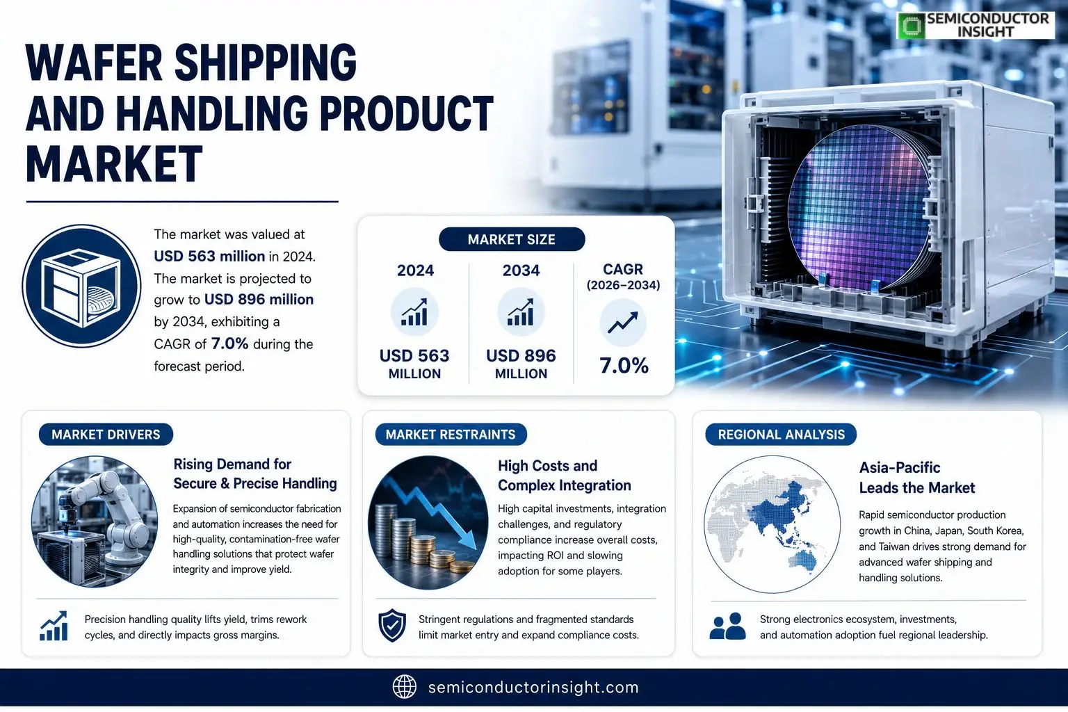
Wafer Shipping and Handling Product market size was valued at USD 563 million in 2024. The market is projected to grow from USD 563 million in 2024 to USD 896 million by 2034, exhibiting a CAGR of 7.0% during the forecast period.
Wafer Shipping and Handling Products comprise containers, transfer boxes, transport cassettes, carrier tapes, and protective fixtures engineered to store, move, and safeguard silicon wafers across fabrication stages and inter‑plant logistics. Front‑opening wafer transfer boxes (FOUPs) are employed within cleanroom manufacturing lines; front‑opening wafer transport boxes (FOSBs) enable inter‑facility movement; wafer flower cassettes support cleaning operations; carrier tapes facilitate automated handling on conveyor systems.
MARKET DRIVERS
Technology Advancement and Reliability Demands
In semiconductor fabrication, even a single micro‑crack can invalidate thousands of devices. Advanced packaging solutions now require protective carriers that preserve wafer integrity during transport across distributed fabs and suppliers. The rise of high‑frequency RF products has amplified the need for carriers that maintain stack‑up precision, driving adoption of engineered polymer blends and engineered thermoplastic composites.
High‑Purity Environments and Shrinkage of Interfaces
Cleanroom certification levels have tightened as photolithography shifts toward EUV lithography, demanding more stringent particulate control. Wafer carriers that incorporate modular dust‑gate technology reduce rework rates by up to 30 % and lock in first‑pass yield, a metric executives now plot against portfolio profitability. Coupled with the industry’s trend toward single‑use, recyclable packaging, these forces are converging to raise the baseline cost of handling products.
➤ Precision handling quality lifts yield, trims rework cycles, and directly impacts gross margins.
Capital expenditures for new shipping lines and equipment are offset by lean manufacturing drives and programmable logistics. Decision makers are increasingly skewing budgets toward modular solutions that can scale with production bursts, ensuring that Wafer Shipping and Handling Product Market continues to evolve.
MARKET CHALLENGES
Complex Integration and Cost Pressures
Integrating new carrier modules into legacy cleanroom lines demands training, tooling updates and downtime. These “overhead” costs compel plant operators to justify spending against hard ROI figures, often shortening the payback window for new handling systems. The incremental cost of specialized packaging varies regionally, making sourcing a complicated calculus.
Other Challenges
Supply Chain Instability
Volatility in polymer raw material pricing and lead times disrupt production planning, limiting the ability to lock in volume discounts and meet aggressive shipment schedules.In addition, the fragmented nature of compliance standards across jurisdictions forces firms to double‑up on certification, eroding the economies of scale that most companies depend on.
MARKET RESTRAINTS
Regulatory Hurdles and Market Fragmentation
Stringent safety and environmental regulations covering flammable materials, hazardous waste handling and shipment labeling impose tight margins on packaging manufacturers. The lack of a standard for wafer carrier certification further complicates market entry for new players, especially those focused on niche or regional solutions.High upfront capital requirements for design, testing and manufacturing of compliant carriers mean that only well‑capitalised enterprises can sustain long‑term growth, constraining broader market participation.
MARKET OPPORTUNITIES
Emerging Markets and Green Shipping Innovations
Rapid industrialisation in Asia‑Pacific and Eastern Europe is creating new fabs that increasingly demand modern, reliable handling infrastructure. Smart sensing embedded in carrier modules is producing a data‑driven service layer that streams real‑time conditions to plant analytics platforms—a trend that opens lucrative aftermarket revenue streams for providers.Parallel to economic forces, investors and governments are championing sustainability metrics. Carriers that boast lower carbon footprints, recyclable materials and zero‑waste manufacturing are poised to capture subsidies and differentiation in buyer portfolios, granting early pioneers a competitive moat.
Wafer Shipping and Handling Product Market Trends
Rising Demand for Front-Opening Wafer Transfer Boxes
Across the semiconductor value chain, the push toward larger‑diameter wafers and tighter yield curves has amplified the need for high‑precision transfer solutions. Front‑opening wafer transfer boxes (FOUPs) now dominate the handling landscape because they allow sealed, dry transfer between fabrication steps and inter‑plant logistics. The interplay of increased wafer size and stricter cleanliness requirements has made FOUPs indispensable in cleanroom environments, propelling demand for more robust, lightweight designs that reduce handling time while maintaining contamination control. Over recent years, FOUPs have expanded from 200mm to 300mm footprints, trimming cycle times by roughly twenty percent and enabling higher throughput on advanced process nodes. Lightweight polymer composites have replaced traditional steel frames, delivering weight reductions of up to fifteen percent that significantly cut transportation costs and lower the environmental footprint of inter‑factory flows. Furthermore, newer sealing technologies employ advanced polymers and micro‑sealants that mitigate particulate ingress, a crucial safeguard for sub‑seven‑nanometre nodes where even trace contamination can throttle yield. Together, these innovations demonstrate that Wafer Shipping and Handling Product Market’s evolution is tightly coupled to the escalating complexity of semiconductor fabrication.
Other Trends
Automation of Wafer Transport Using Robotics
Leveraging stationary and mobile robotic platforms, many OEMs are integrating automated wafer transport into production lines to mitigate human error and improve throughput. The use of vibration‑isolated gantries and vision‑based pick‑and‑place robots ensures precise positioning within micron tolerances while reducing the need for manual intervention. This shift toward automation not only shortens cycle times but also lowers contamination incidents, which is critical for high‑yield production of 300mm wafers used in photonics and advanced logic nodes. In addition, real‑time condition monitoring embedded in robotic arms detects subtle shifts in load distribution or wrist speed, allowing proactive maintenance that precludes spillage or wafer misplacement. The integration of AI‑driven scheduling systems further optimises routing across multiple fabs, balancing load and reserving high‑priority items for tighter deadlines. As a consequence, overall handling reliability climbs while maintenance windows shrink, giving fabs a competitive edge in scheduling and cost control.
Regional Divergence in Adoption Rates
North America and Europe maintain the highest penetration of FOUPs and automated handling, driven by entrenched photolithography and high‑performance computing fabs. In contrast, the Asia Pacific region, despite its massive floor space, still grapples with fragmented supply chains and uneven regulatory compliance, leading to a modest 2 % decline in handling efficiency between 2021 and 2022. Manufacturers that invest in localized packaging expertise and build end‑to‑end supply resilience can capture growing share in emerging markets, especially as demand for 200mm wafer re‑use and edge‑device manufacturing accelerates. The ripple effect is evident in logistics cost structures: fabs that standardise on FOUPs experience lower freight expenditures and benefit from reduced downtime associated with manual handling. For suppliers, this trend translates into a premium on modular, scalable handling solutions that can be tailored to regional design rules and compliance frameworks, positioning those with rapid prototyping and local assembly capabilities at a competitive advantage as the wafer ecosystem transitions toward more diversified node architectures.
COMPETITIVE LANDSCAPE
Key Industry Players
Wafer Shipping and Handling Product Market Competitive Landscape
Entegris dominates the wafer shipping and handling arena, commanding roughly one‑third of revenue despite a highly fragmented supply chain. Its strategy of bundling FOUPs, FOSBs and wafer‑flower cassettes within a single, scalable platform has driven a lift in margin and customer lock‑in. The firm’s geographic footprint spans the entire semiconductor ecosystem, with a sizeable presence in North America, Europe and Asia‑Pacific, enabling it to capture the most lucrative equipment‑linked contracts. In addition, Entegris’ investment in 3‑D packaging and advanced photolithography use‑cases has expanded the relevance of its handling products beyond traditional logic and memory fabs, cultivating new revenue streams. This concentration of sales power is clearly reflected in the company’s upward‑trending revenue trajectory, its position as the most cited supplier in industry surveys, and its ability to negotiate premium pricing for OEM modules. Combined, these dynamics cement Entegris as the de facto benchmark in both performance and scale for wafer shipping solutions. Additionally, Entegris’ recent acquisition of a wafer‑handling tech start‑up has broadened its product palette, enabling rapid prototyping for sub‑10 nm processes, thereby locking in early‑adopter clients.Shin‑Etsu Polymer continues to carve out a niche in high‑temperature wafer carriers, while Miraial’s lightweight FOSB designs attract memory fabs that prioritize throughput over cost. In the small‑batch segment, Chuang King Enterprise and Gudeng Precision deliver custom flower cassettes for 300 mm wafer cleaning, catering to AI and automotive semiconductor nodes. The ePAK group offers value‑added ancillary services such as RF shielding and moisture control, which are increasingly demanded by an ever‑shifting supply chain landscape. In contrast, the Korean conglomerate 3S Korea excels in cost‑effective, high‑volume transport boxes for emerging Middle‑East and African fabs. Dainichi Shoji, Fuji Bakelite, Seyang Electronics and Shenzhen Dong Hong Xin Industrial round out the competitive field, each focusing on specific subsegments such as cleanroom compliance, environmental protection and tie‑in with fifth‑generation (5G) equipment suppliers. Together, these players construct a mosaic of specialized solutions that not only meet divergent fab needs but also expose geographic concentration risks as the industry recycles around the most advanced nodes, creating strategic opportunities for vertical integration and niche differentiation. Their relatively lightweight capital structures and agility allow them to respond rapidly to regional demand shifts, particularly in Latin America and Southeast Asia, where fab expansion is accelerating.
List of Key Wafer Shipping and Handling Product Companies Profiled
- Entegris
- Shin‑Etsu Polymer
- Miraial
- Chuang King Enterprise
- Gudeng Precision
- ePAK
- 3S Korea
- Dainichi Shoji
- Fuji Bakelite
- Seyang Electronics
- Shenzhen Dong Hong Xin Industrial
- Amkor Technology
- ASE Group
Segment Analysis:
| Segment Category | Sub-Segments | Key Insights |
| By Type |
|
Wafer Transport Boxes
|
| By Application |
|
300mm Wafer
|
| By End User |
|
Semiconductor OEM
|
| By Wafer Size |
|
400mm Wafer
|
| By Handling Equipment |
|
FOUP
|
Regional Analysis: Wafer Shipping and Handling Product Market
Europe
Capital expenditure trends in Europe have shifted toward modular, scalable handling platforms that can be upgraded as fabs mature to newer nodes. Firms favour contract‑based procurement to tame upfront costs while seeking financing solutions that allow rapid deployment of clean‑room compatible carriers. This shift indicates that investors prioritise flexibility and long‑term cost savings over sheer volume procurement.
Logistics for wafer carriers in Europe has become increasingly differentiated, with a move toward ultra‑reliable, low‑latency transportation networks integrated with on‑site handling systems. The region’s dense industrial corridors and high‑speed rail networks provide an infrastructure advantage, yet they impose strict schedule constraints that manufacturers must meet to avoid runaway downtime. End‑to‑end planning is finalised close to operational launch to synchronize with process changes.
Regulatory expectations across the EU tighten regarding chemical use, waste disposal, and energy efficiency in wafer handling processes. Manufacturers must document cradle‑to‑grave lifecycle assessments for each handling unit, pushing suppliers to adopt green materials and circular business models. The result is a preference for reusable metal trays with embedded sensors that reduce single‑use plastics while enabling real‑time monitoring of contamination levels.
Innovation has pivoted around digital twins and predictive analytics. By simulating the transport cycle in a virtual environment, SME operators can identify bottlenecks before they occur, saving time and controlling defect rates. Suppliers increasingly incorporate AI‑based fault alerts into carrier firmware, which feeds directly into plant management dashboards, assuring compliance and continuous improvement.
North America
The North American wafer shipping and handling product market exhibits a mature supply chain underpinned by advanced fabrication hubs in California, Texas, and Arizona. Precision handling systems demand sub‑nanometer tolerances, prompting the adoption of CMMS‑integrated racks that automate wafer transport within cleanrooms. Regulatory frameworks around hazardous materials disposal and radiation safety drive procurement toward ISO‑certified carriers that meet environmental and safety mandates. Suppliers must innovate in blendable photon‑scalable carriers and AI‑guided route planning to align with a compliance‑heavy, technology‑savvy market.
Asia‑Pacific
Asia‑Pacific remains the most dynamic hotspot for wafer shipping and handling solutions, largely due to rapid fab expansion in China, Japan, and South Korea. Market participants face a dual imperative: accommodating high‑volume production while maintaining stringent contamination controls. This drives a shift toward automated, scalable handling lines that re‑target to new process nodes. Local regulations on particulate monitoring and chemical usage compel manufacturers to adopt smart carriers with embedded sensors that feed data to plant dashboards. Vendors focus on modular, AI‑enhanced systems that deploy quickly and comply with local and international standards. Wafer Shipping and Handling Product Market in this region rewards speed and adaptability.
South America
South American wafer handling dynamics are characterised by growing investment in semiconductor export clusters, especially in Chile and Brazil. Growth is propelled by a push for localized production to reduce import dependence and enhance resilience. Limited local expertise and harsh climate conditions create unique handling challenges, prompting a preference for rugged, climate‑controlled carriers that operate reliably across temperature swings. The evolving regulatory framework enforces stricter particulate and chemical safety thresholds, driving operators toward suppliers offering certified, low‑contamination routing equipment. Tiered handling solutions that expand with plant growth provide scalability without substantial capital outlays.
Middle East & Africa
Middle East and Africa’s wafer handling market is shifting from reactive to proactive as integrated fab projects increase in Saudi Arabia, UAE, and emerging African nations. High ambient temperatures and dust‑laden environments steer operators toward hermetically sealed carriers with HEPA‑grade filtration, ensuring wafer integrity during transport. Policy focus on local manufacturing and technology transfer mandates supplier compliance with regional safety and sustainability standards. Consequently, manufacturers gravitate toward modular carrier platforms featuring data logging and low‑energy consumption, enabling them to meet operational efficiency targets and ESG reporting requirements.
Report Scope
This market research report provides a comprehensive analysis of the Wafer Shipping and Handling Product Market , covering the forecast period 2026–2034. It offers detailed insights into market dynamics, technological advancements, competitive landscape, and key trends shaping the industry.
Key focus areas of the report include:
- Market Overview: The report begins with an overview outlining its current market scenario, key growth indicators, and industry transformation drivers. It discusses macroeconomic factors, demand–supply balance, regulatory landscape, and the strategic role of semiconductors in powering advancements across industries such as automotive, telecommunications, consumer electronics, and industrial automation.
- Market Size & Forecast: Historical data and future projections for revenue, unit shipments, and market value across major regions and segments.
- Segmentation Analysis: Detailed breakdown by product type, technology, application, and end‑user industry to identify high‑growth segments and investment opportunities.
- Regional Insights: Insights into market performance across North America, Europe, Asia-Pacific, Latin America, and the Middle East & Africa, including country‑level analysis where relevant.
- Competitive Landscape: Profiles of leading market participants, including their product offerings, R&D focus, manufacturing capacity, pricing strategies, and recent developments such as mergers, acquisitions, and partnerships.
- Technology Trends & Innovation: Assessment of emerging technologies, integration of AI/IoT, semiconductor design trends, fabrication techniques, and evolving industry standards.
- Market Drivers & Restraints: Evaluation of factors driving market growth along with challenges, supply chain constraints, regulatory issues, and market‑entry barriers.
- Stakeholder Insights: Insights for component suppliers, OEMs, system integrators, investors, and policymakers regarding the evolving ecosystem and strategic opportunities.
Primary and secondary research methods are employed, including interviews with industry experts, data from verified sources, and real‑time market intelligence to ensure the accuracy and reliability of the insights presented.
FREQUENTLY ASKED QUESTIONS:
What is the current market size of Wafer Shipping and Handling Product Market?
-> Wafer Shipping and Handling Product Market was valued at USD 563 million in 2024 and is projected to reach USD 896 million by 2034, at a CAGR of 7.0%
Which key companies operate in Wafer Shipping and Handling Product Market?
-> Key players include Entegris, Shin‑Etsu Polymer, Miraial, Chuang King Enterprise, Gudeng Precision, ePAK, 3S Korea, Dainichi Shoji, Fuji Bakelite, Seyang Electronics, and Shenzhen Dong Hong Xin Industrial.
What are the key growth drivers?
-> Key growth drivers include expanding semiconductor manufacturing, advanced wafer handling technologies, demand for high‑quality protection, and increasing automation in supply chains.
Which region dominates the market?
-> Asia‑Pacific remains the dominant region, driven by rapid semiconductor production and strong industry activity in China, Japan, and South Korea.
What are the emerging trends?
-> Emerging trends include automation and robotics, advanced packaging materials, streamlined logistics solutions, and sustainable packaging practices for wafers.

Get Sample Report PDF for Exclusive Insights
Report Sample Includes
- Table of Contents
- List of Tables & Figures
- Charts, Research Methodology, and more...
 Download Sample Report PDF