
Key Statistics
Key Takeaways
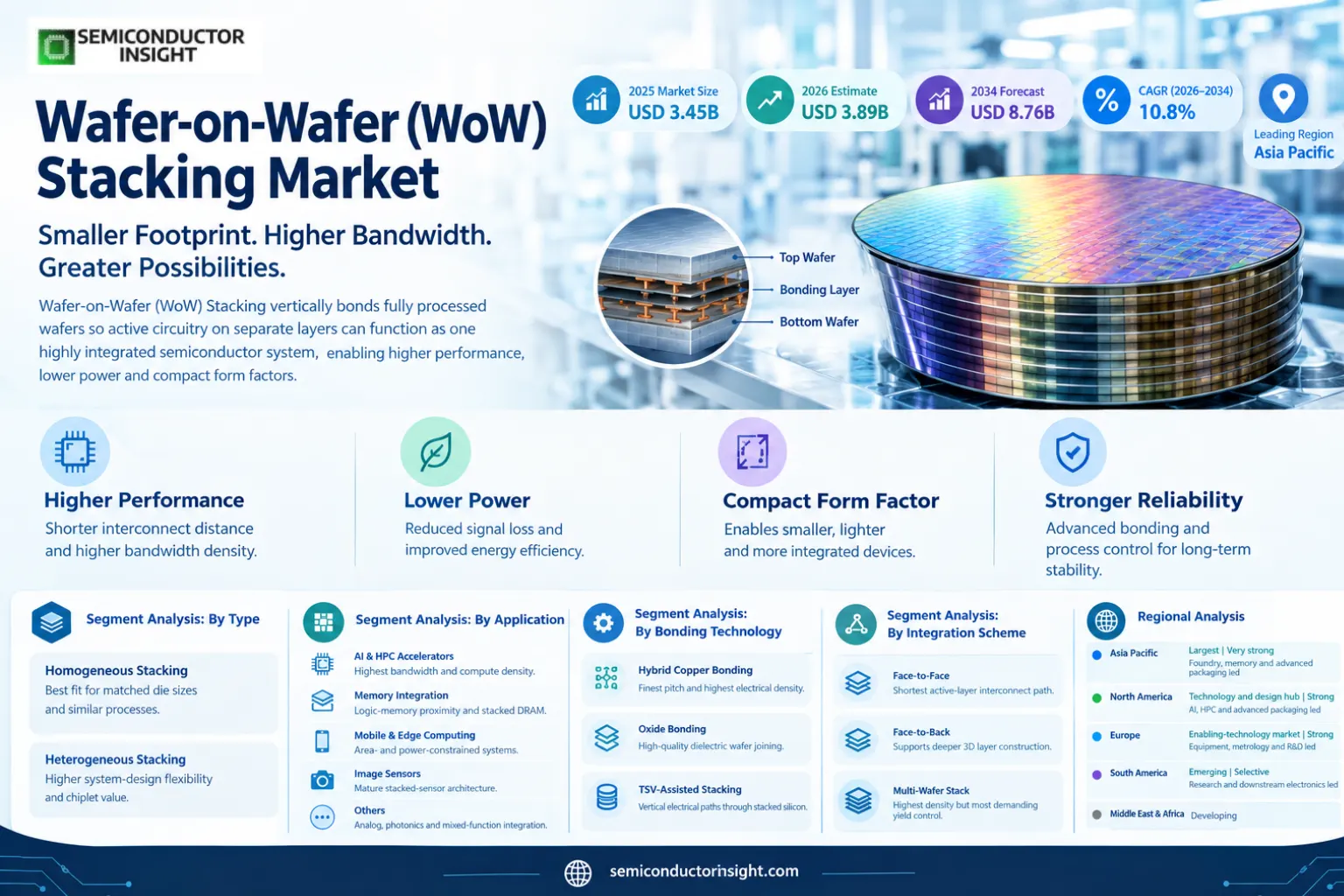
- The market is valued at USD 3.45 billion in 2025 and is projected to reach USD 8.76 billion by 2034, representing a 10.8% CAGR over 2026–2034.
- Homogeneous Wafer Stacking is a major product segment, while adjacent variants are expanding as performance, integration and cost requirements evolve.
- AI & HPC Accelerators is a leading application area, supported by demand across Memory Integration, Mobile & Edge Computing.
- Asia Pacific is the largest market in 2025 based on current demand, manufacturing concentration and ecosystem maturity.
Wafer-on-Wafer (WoW) Stacking Market Overview
Wafer-on-Wafer (WoW) Stacking vertically bonds fully processed wafers so active circuitry on separate layers can function as one highly integrated semiconductor system. The approach shortens interconnect distance, raises bandwidth density and reduces package footprint, making it particularly valuable where monolithic scaling no longer delivers sufficient performance or energy efficiency. Commercial adoption of Wafer-on-Wafer (WoW) Stacking products therefore depends on system-level productivity, integration requirements, reliability expectations and the economics of replacing established alternatives in real operating environments.
Commercial adoption is accelerating as hybrid bonding matures and AI, HPC and advanced-memory systems require much denser chip-to-chip connectivity. WoW is most economical when wafers have compatible die sizes and high known-good yield, while chip-on-wafer alternatives are often preferred when die size or process mix differs substantially. Suppliers that translate technical improvements into measurable gains in efficiency, uptime, cost, throughput or workflow simplicity are better positioned to win long-duration programs and repeat purchases.
Segment Analysis: By Type
Homogeneous stacking is attractive when wafers use compatible die sizes and process technologies, while heterogeneous stacking creates greater system value by combining logic, memory, analog, sensor or I/O functions manufactured on different nodes. Heterogeneous architectures are the stronger long-term growth area because they let designers optimize each layer independently rather than forcing every function onto one monolithic process.
| Segment | Market Relevance |
|---|---|
| Homogeneous Wafer Stacking | Best fit for matched die sizes and similar processes. |
| Heterogeneous Wafer Stacking | Highest system-design flexibility and chiplet value. |
Segment Analysis: By Application
AI and HPC accelerators are the most important high-value applications because model size and memory traffic make short vertical interconnects economically valuable. Memory integration, mobile compute and image sensors also benefit from smaller footprint, lower latency and higher bandwidth. Image-sensor stacking is a mature proof point that helps validate broader wafer-bonding infrastructure.
| Segment | Market Relevance |
|---|---|
| AI & HPC Accelerators | Highest bandwidth and compute-density demand. |
| Memory Integration | Logic-memory proximity and stacked DRAM use. |
| Mobile & Edge Computing | Area- and power-constrained systems. |
| Image Sensors | Established commercial stacked-sensor architecture. |
| Others | Specialty analog, photonics and mixed-function integration. |
Segment Analysis: By Bonding Technology
Hybrid copper bonding is the central technology trend because direct Cu-to-Cu connections can achieve much finer pitch than solder microbumps while reducing electrical resistance. Oxide bonding provides mechanical alignment and dielectric connection, while TSV-assisted stacks move signals and power vertically across wafers and enable multi-layer architectures. Within this segment, customers increasingly compare lifecycle support, qualification requirements, integration effort and total ownership cost rather than relying on a single specification or upfront price.
| Segment | Market Relevance |
|---|---|
| Hybrid Copper Bonding | Finest pitch and highest electrical density. |
| Oxide Bonding | High-quality dielectric wafer joining. |
| TSV-Assisted Stacking | Vertical electrical paths through stacked silicon. |
Segment Analysis: By Integration Scheme
Face-to-face bonding minimizes interconnect length between active layers, face-to-back stacking enables additional vertical layers, and multi-wafer stacks create the highest integration density. Yield management becomes more important as stack depth increases because one defective wafer can affect the economics of the entire bonded structure. Within this segment, customers increasingly compare lifecycle support, qualification requirements, integration effort and total ownership cost rather than relying on a single specification or upfront price.
| Segment | Market Relevance |
|---|---|
| Face-to-Face | Shortest active-layer interconnect path. |
| Face-to-Back | Supports deeper 3D layer construction. |
| Multi-Wafer Stack | Highest density but most demanding yield control. |
Regional Analysis
Asia Pacific leads because Taiwan, South Korea and Japan combine the largest advanced foundry, memory and packaging ecosystems. North America remains a key architecture and technology-development region, while Europe contributes bonding equipment, metrology and research capability. Regional share also reflects supplier depth, engineering support, manufacturing concentration and the speed at which new Wafer-on-Wafer (WoW) Stacking designs can move from evaluation into repeat deployment.
| Region | Position | Growth | Profile |
|---|---|---|---|
| Asia Pacific | Largest | Very strong | Foundry, memory and advanced packaging led |
| North America | Technology and design hub | Strong | AI, HPC and advanced packaging led |
| Europe | Enabling-technology market | Strong | Equipment, metrology and R&D led |
| South America | Emerging | Selective | Research and downstream electronics led |
| Middle East & Africa | Developing | Selective | Technology investment and research led |
Detailed Regional Blocks
Why does Asia Pacific matter in this market?
Asia Pacific leads because TSMC, Samsung and regional packaging suppliers operate the most advanced 3D-integration manufacturing ecosystems. AI accelerators and stacked memory create strong demand for hybrid bonding, TSVs and high-precision wafer alignment. In Asia Pacific, procurement decisions also depend on service coverage, qualification resources, logistics and long-term availability, so ecosystem maturity can materially influence adoption even when core technology performance is similar.
| Country / Market | Role | Context |
|---|---|---|
| Taiwan | Global foundry hub | TSMC SoIC and advanced packaging drive commercial adoption. |
| South Korea | Memory and foundry hub | Samsung combines HBM, logic and 3D integration capability. |
| Japan | Materials and equipment hub | Bonding, metrology and specialty materials support scale-up. |
- TSMC states that SoIC-X wafer-on-wafer integrates homogeneous or heterogeneous wafers using tight bonding pitch and thin TSVs.
- TSMC’s 2025 annual report says 3 nm SoIC stacking entered volume production in 2025.
- Samsung’s 3D Packaging roadmap includes hybrid copper bonding for denser vertical integration.
Why does North America matter in this market?
North America is strategically important because leading AI and processor companies design systems that need ultra-dense die-to-die links. Intel Foundry’s Foveros Direct architecture also demonstrates direct copper hybrid bonding for stacked chiplets and wafers. In North America, procurement decisions also depend on service coverage, qualification resources, logistics and long-term availability, so ecosystem maturity can materially influence adoption even when core technology performance is similar.
| Country / Market | Role | Context |
|---|---|---|
| United States | Largest regional technology base | AI, processor and foundry R&D drive adoption. |
| Canada | Research niche | 3D integration and packaging research support development. |
- Intel Foundry positions Foveros Direct 3D around copper-to-copper hybrid bonding for high-density, low-resistance interconnects.
- Intel states first-generation Foveros Direct uses 9 µm copper pitch, with later generations moving toward 3 µm.
- AI/HPC workloads create the strongest economic incentive for short high-bandwidth vertical links.
Why does Europe matter in this market?
Europe plays an enabling role through semiconductor-equipment, bonding and research organizations. Regional value capture is concentrated in process equipment, inspection, materials and collaborative 3D-integration development rather than the largest production wafer volumes. In Europe, procurement decisions also depend on service coverage, qualification resources, logistics and long-term availability, so ecosystem maturity can materially influence adoption even when core technology performance is similar.
| Country / Market | Role | Context |
|---|---|---|
| Netherlands | Semiconductor equipment hub | Advanced equipment ecosystem supports 3D integration. |
| Belgium | R&D hub | imec supports hybrid-bonding research and process development. |
| Germany | Materials and equipment | Precision manufacturing supports packaging infrastructure. |
- European research programs are focused on fine-pitch bonding, alignment accuracy and thermal management.
- Hybrid bonding requires extremely flat, clean and defect-free wafer surfaces.
- Metrology becomes more critical as bonding pitch moves into single-digit micrometers.
Why does South America matter in this market?
South America remains a small direct market because advanced wafer-level 3D integration requires major foundry and packaging infrastructure. Current participation is mainly through imported advanced semiconductors and research collaboration. In South America, procurement decisions also depend on service coverage, qualification resources, logistics and long-term availability, so ecosystem maturity can materially influence adoption even when core technology performance is similar.
| Country / Market | Role | Context |
|---|---|---|
| Brazil | Largest regional research base | Academic semiconductor programs create limited direct activity. |
| Argentina | Research niche | Commercial WoW manufacturing is absent. |
- Most regional value is consumed inside imported advanced devices.
- High capital intensity limits local WoW manufacturing.
- Research partnerships are more realistic than independent high-volume deployment.
Why does Middle East & Africa matter in this market?
Middle East and Africa are early-stage direct markets. Israel contributes semiconductor design and research, while Gulf technology initiatives could support future advanced-packaging investment if local fabrication ecosystems deepen. In Middle East & Africa, procurement decisions also depend on service coverage, qualification resources, logistics and long-term availability, so ecosystem maturity can materially influence adoption even when core technology performance is similar.
| Country / Market | Role | Context |
|---|---|---|
| Israel | Semiconductor design hub | Advanced chip design creates indirect demand. |
| United Arab Emirates | Technology-investment niche | Long-term packaging initiatives could develop. |
| Saudi Arabia | Emerging semiconductor strategy | Current direct WoW demand is limited. |
- WoW requires high-yield wafer fabrication before bonding economics become attractive.
- Supplier proximity is important because alignment and bonding processes are tightly controlled.
- Near-term regional demand is primarily indirect through imported AI and high-performance processors.
Competitive Landscape
TSMC, Samsung Electronics, Intel Foundry, ASE, GlobalFoundries, STMicroelectronics and specialized bonding-equipment suppliers compete through hybrid-bonding pitch, yield, TSV integration, thermal design and compatibility with broader advanced-packaging platforms.
| Company | Competitive Context |
|---|---|
| TSMC | SoIC supports both chip-on-wafer and wafer-on-wafer integration with hybrid bonding and TSVs. |
| Samsung Electronics | 3D Packaging / former X-Cube roadmap includes micro-bump and hybrid copper bonding architectures. |
| Intel Foundry | Foveros Direct 3D provides direct Cu-to-Cu hybrid-bonded stacked integration. |
| ASE Group | Relevant participant with products, IP or system-level presence in this market. |
| GlobalFoundries | Relevant participant with products, IP or system-level presence in this market. |
| STMicroelectronics | Relevant participant with products, IP or system-level presence in this market. |
| Amkor Technology | Relevant participant with products, IP or system-level presence in this market. |
| Besi | Relevant participant with products, IP or system-level presence in this market. |
Production Capacity Analysis
WoW capacity depends on front-end wafer yield, wafer thinning, TSV formation, CMP flatness, hybrid-bonding equipment, precision alignment and post-bond test. Unlike conventional packaging, the economic loss from bonding low-yield wafers can be severe, so known-good-wafer strategies and mature process control are essential. Scaling output without degrading consistency requires stable upstream materials, disciplined process control and final testing that catches performance drift before products reach high-value customer systems.
Capacity is concentrated at leading foundries and advanced-packaging facilities because sub-10-micron bonding demands specialized tools and metrology. Expansion therefore requires coordinated investment across wafer fabrication, bonding and inspection rather than adding only package-assembly equipment. Second-source planning and regional technical support therefore become increasingly important as deployments expand and buyers seek supply continuity without repeating lengthy qualification work.
Market Dynamics
The market is moving from microbump-based stacking toward hybrid copper bonding because pitch reduction improves bandwidth density and lowers interconnect resistance. This change is especially important for AI and memory systems where electrical links between layers can number in the thousands or millions. This is changing competitive behavior because vendors increasingly sell system-level value, workflow integration and lifecycle economics rather than an isolated component specification.
WoW competes with chip-on-wafer and chiplet packaging rather than replacing them. Wafer-on-wafer offers superior throughput when die size and yield match, while die-level assembly provides greater flexibility for heterogeneous die sizes and known-good-die selection. Buyers consequently evaluate total ownership cost, qualification effort and roadmap stability across the life of a program instead of focusing only on initial purchase price.
Market Drivers
AI and HPC bandwidth
Advanced packaging demand
Hybrid bonding maturity
Memory integration
Market Restraints
Yield multiplication
Thermal management
Capital intensity
Die-size matching
Market Opportunities
Sub-5µm hybrid bonding
AI accelerator stacks
3D sensor systems
Multi-wafer integration
Supply Chain Analysis
The value chain combines leading-edge wafer fabrication, TSV processing, CMP and surface preparation, precision wafer alignment, hybrid bonding, thinning, test and final package integration. Yield control connects every stage. Traceability and coordination between component suppliers, integrators and end users are important because failures found late in the chain can be far more expensive than the underlying part itself.
| Stage | Role |
|---|---|
| Processed wafers | Logic, memory or sensor wafers are completed and electrically characterized. |
| Surface preparation and TSVs | Wafers are planarized, metallized and prepared for vertical links. |
| Hybrid wafer bonding | Wafers are aligned and bonded at fine pitch. |
| Post-bond thinning and package integration | The stack is thinned, tested and integrated into final advanced packages. |
Recent Developments
Report Scope & Segmentation
| Base Year | 2025 |
| Estimated Year | 2026 |
| Forecast Year | 2034 |
| Forecast Period | 2026–2034 |
| Market Size, 2025 | USD 3.45 billion |
| Projected Market Size, 2034 | USD 8.76 billion |
| CAGR, 2026–2034 | 10.8% |
| Largest Market in 2025 | Asia Pacific |
| Segmentation Coverage | By Type, By Application, By Bonding Technology, By Integration Scheme |
Frequently Asked Questions
What is the Wafer-on-Wafer (WoW) Stacking market size in 2025?
The market is valued at USD 3.45 billion in 2025.
What is the projected Wafer-on-Wafer (WoW) Stacking market size by 2034?
The market is projected to reach USD 8.76 billion by 2034.
What is the CAGR for the Wafer-on-Wafer (WoW) Stacking market from 2026 to 2034?
The market is projected to expand at a 10.8% CAGR from 2026 to 2034.
Which region leads the Wafer-on-Wafer (WoW) Stacking market?
Asia Pacific is the largest market in 2025.
What are the main types in the Wafer-on-Wafer (WoW) Stacking market?
Key types include Homogeneous Wafer Stacking, Heterogeneous Wafer Stacking.
What are the main applications for Wafer-on-Wafer (WoW) Stacking?
Major applications include AI & HPC Accelerators, Memory Integration, Mobile & Edge Computing, Image Sensors, Others.
What is driving growth in the Wafer-on-Wafer (WoW) Stacking market?
Dense vertical interconnect reduces latency and power between compute and memory layers.
What is a key restraint for the Wafer-on-Wafer (WoW) Stacking market?
A defective wafer can reduce the value of the bonded stack.
Which companies are important in the Wafer-on-Wafer (WoW) Stacking market?
Important participants include TSMC, Samsung Electronics, Intel Foundry, ASE Group, GlobalFoundries, STMicroelectronics.
What opportunity is emerging in the Wafer-on-Wafer (WoW) Stacking market?
Finer pitch can unlock much higher vertical bandwidth.
Research Sources & Evidence Base
View research sources used for this overview.
- TSMC — TSMC-SoIC: Wafer-on-wafer and chip-on-wafer 3D integration architecture and benefits.
- Intel Foundry — Advanced Packaging: Foveros Direct 3D hybrid bonding and stacked integration.
- Samsung Semiconductor — Advanced Packaging: Current 3D Packaging and hybrid copper bonding roadmap.

Get Sample Report PDF for Exclusive Insights
Report Sample Includes
- Table of Contents
- List of Tables & Figures
- Charts, Research Methodology, and more...
 Download Sample Report PDF

