
Wafer Bonding (Hybrid, Direct, Adhesive) Services Market Insights
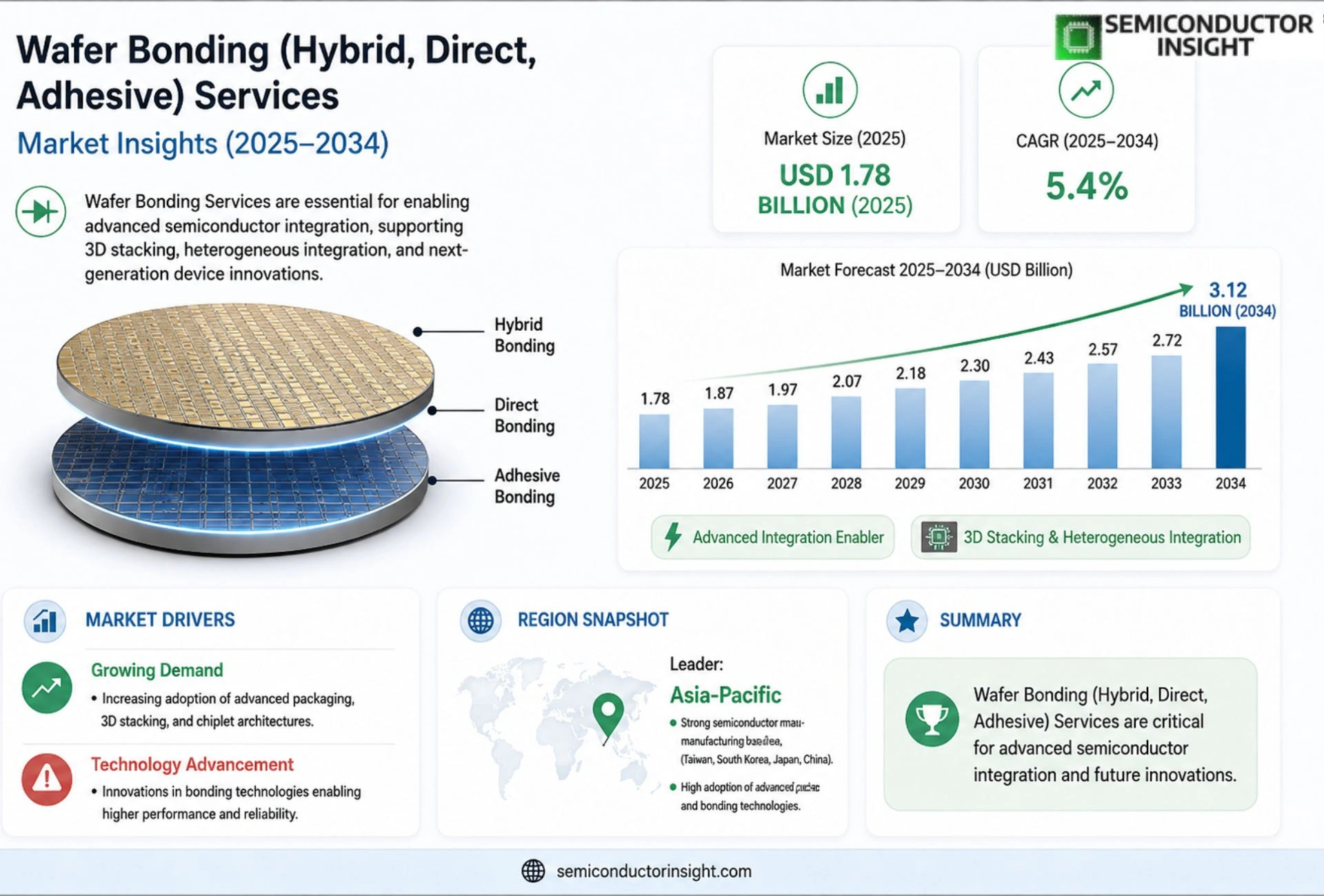
Global Wafer Bonding (Hybrid, Direct, Adhesive) Services Market size was valued at USD 1.78 billion in 2025. The market is projected to grow from USD 1.78 billion in 2025 to USD 3.12 billion by 2034, exhibiting a CAGR of 5.4% during the forecast period.
Wafer bonding services comprise three principal techniques: hybrid bonding, which merges dielectric and metal interconnects at the atomic level; direct bonding, a silicon‑to‑silicon process that requires no intermediate layers; and adhesive bonding, which utilizes polymeric adhesives for low‑temperature attachment. These methods enable high‑density integration of MEMS sensors, advanced logic chips, and heterogeneous semiconductor packages.
The market is experiencing rapid growth because demand for heterogeneous integration in smartphones, automotive electronics, and IoT devices is soaring; however, high capital expenditure for precision equipment remains a challenge. Furthermore, increased R&D spending by leading foundries and the rollout of 5G/6G networks are accelerating adoption of advanced wafer bonding processes.
MARKET DRIVERS
Demand from Advanced Semiconductor Devices
The rapid expansion of 5G infrastructure and AI‑enabled edge computing is fueling higher demand for advanced semiconductor packaging. Wafer Bonding (Hybrid, Direct, Adhesive) Services Market benefits from the need for miniaturized, high‑performance modules that require reliable interconnects and thermal management.
Cost‑Effective Manufacturing Strategies
Manufacturers are adopting hybrid and direct bonding techniques to reduce cycle time and eliminate the need for costly intermediate materials. This shift improves yield and lowers total cost of ownership, making wafer bonding services an attractive option for high‑volume production.
➤ Industry surveys indicate that over 60% of fab operators plan to increase investment in wafer bonding equipment within the next two years.
In addition, government incentives for domestic semiconductor fabs are strengthening the supply chain, further accelerating adoption of comprehensive wafer bonding solutions.
MARKET CHALLENGES
Technical Complexity and Integration
Integrating hybrid, direct, and adhesive bonding processes into existing production lines often requires significant re‑engineering. The steep learning curve can delay time‑to‑market for new device architectures, especially for smaller players lacking dedicated R&D resources.
Other Challenges
Material Compatibility
Achieving reliable bonds across diverse substrate materials—such as silicon, glass, and compound semiconductors—remains a critical hurdle. Mismatched coefficients of thermal expansion can lead to stress‑induced failures if not carefully managed.
MARKET RESTRAINTS
Regulatory and Environmental Constraints
Stringent environmental regulations on chemical usage and waste disposal limit the adoption of certain adhesive bonding formulations. Compliance costs can deter smaller fabs from scaling up their wafer bonding capabilities.
MARKET OPPORTUNITIES
Emerging Applications in Photonics and MEMS
Growth in photonic integrated circuits, micro‑electromechanical systems, and quantum computing devices presents new avenues for wafer bonding service providers. These segments demand ultra‑precise alignment and low‑defect bonding, creating premium‑price opportunities for specialized service offerings.
Trends
Rapid Adoption in Heterogeneous Integration
Wafer Bonding (Hybrid, Direct, Adhesive) Services Market is witnessing accelerated uptake as manufacturers target higher levels of functional density in advanced semiconductor packages. Hybrid bonding delivers atomic‑level interconnects, while direct bonding eliminates intermediate layers, and adhesive bonding supports low‑temperature assembly. Together, these techniques enable seamless stacking of MEMS sensors, high‑performance logic dies, and heterogeneous modules that meet the bandwidth demands of 5G and forthcoming 6G networks. The confluence of smartphone miniaturization, automotive radar expansion, and IoT edge computing is creating a sustained pipeline of design projects that rely on these bonding processes.
Other Trends
Capital Intensity of Precision Equipment
Investments in wafer bonding tools remain a critical barrier for many fab operators. The equipment required for hybrid and direct bonding demands sub‑nanometer surface preparation, inline metrology, and high‑vacuum environments, driving up upfront costs. As a result, only large foundries and specialized service providers are able to amortize the capital efficiently, while smaller players increasingly seek outsourced bonding services to avoid prohibitive expenditures.
Emerging Applications in Automotive and IoT
Automotive electronic control units and advanced driver‑assistance systems are adopting wafer‑bonded solutions to achieve ruggedness and high thermal performance. The need for reliable, compact sensor arrays in autonomous vehicles pushes suppliers toward direct and hybrid bonding for improved signal integrity. Simultaneously, IoT devices benefit from adhesive bonding’s low‑temperature processing, which protects temperature‑sensitive components and shortens time‑to‑market. These sectoral shifts reinforce the strategic importance of Wafer Bonding (Hybrid, Direct, Adhesive) Services Market as a foundational enabler for next‑generation electronic ecosystems.
COMPETITIVE LANDSCAPE
Key Industry Players
Wafer Bonding (Hybrid, Direct, Adhesive) Services Market – Competitive Landscape
Wafer Bonding (Hybrid, Direct, Adhesive) Services Market is currently dominated by a handful of technologically advanced firms that command the majority of high‑volume capacity. ASM International stands out as the market leader, leveraging its patented Hybrid Bond technology and a global network of R&D collaborations with leading foundries such as TSMC and Intel. Toray Industries follows closely, distinguished by its large‑scale Direct Bond facilities and an extensive polymer‑adhesive portfolio that supports low‑temperature assembly for automotive and IoT chips. This concentration of capabilities creates a tiered structure where a few multinational corporations supply end‑to‑end bonding solutions, while a secondary layer of specialized equipment manufacturers and contract service providers feed niche demand from MEMS and sensor manufacturers.
Beyond the top tier, a diverse set of niche players adds depth to the competitive landscape. SUSS MicroTec and Miyachi offer precision wafer‑bonding tools that enable small‑batch and prototype production. Nikon and Applied Materials provide complementary metrology and surface‑preparation services that are critical for defect‑free bonding. Regional specialists such as JX Nippon Mining & Metals, Shindengen, and Shin‑Etsu Chemical focus on adhesive formulations and dielectric bonding for specific market segments, including aerospace and medical devices. The collective presence of these firms sustains innovation while keeping entry barriers moderate for emerging semiconductor manufacturers.
List of Key Wafer Bonding (Hybrid, Direct, Adhesive) Services Companies Profiled
- ASM International
- Toray Industries
- SUSS MicroTec
- Miyachi
- Nikon Corporation
- Applied Materials
- JX Nippon Mining & Metals
- Shin‑Etsu Chemical
- TSMC (Taiwan Semiconductor Manufacturing Company)
- GlobalFoundries
- Intel Corporation
- Samsung Electronics
- SK Hynix
- Broadcom Inc.
- Cambridge Microelectronics
Segment Analysis:
| Segment Category | Sub-Segments | Key Insights |
| By Type |
|
Hybrid Bonding
|
| By Application |
|
MEMS Sensors
|
| By End User |
|
Smartphone Manufacturers
|
| By Technology Maturity |
|
Emerging
|
| By Device Category |
|
RF Modules
|
Regional Analysis:
The North American market is witnessing a surge in demand for advanced wafer bonding techniques to support the development of next-generation semiconductor devices. Hybrid bonding, in particular, is gaining traction for its ability to integrate diverse chiplets with varying process technologies.
The competitive landscape in the US is characterized by a mix of established players and emerging specialists. Key players are focused on expanding their service offerings and enhancing their technological capabilities to meet the evolving needs of the semiconductor industry. Strategic partnerships and acquisitions are common strategies for gaining market share.
The growth of the automotive industry, with its increasing reliance on electronic control units (ECUs) and advanced driver-assistance systems (ADAS), is a significant driver for wafer bonding services. Furthermore, the expansion of data centers and the demand for high-bandwidth communication infrastructure contribute to the market’s growth.
The future outlook for the Wafer Bonding Services Market in North America remains positive, driven by continuous innovation and the increasing complexity of semiconductor devices. The adoption of 3D integration technologies and the integration of advanced materials are expected to further propel market growth in the coming years.
Europe
The European Wafer Bonding Services Market is poised for steady growth, driven by a strong foundation in microelectronics research and development, particularly within countries like Germany, France, and the Netherlands. The region’s focus on sustainable technologies and industrial digitalization is creating demand for advanced packaging solutions that enhance device performance while minimizing power consumption. Several initiatives are underway to bolster Europe’s semiconductor manufacturing capabilities, which is expected to positively impact the wafer bonding services market. The emphasis on high-performance computing and automotive electronics further contributes to the market’s potential. However, challenges related to supply chain disruptions and geopolitical uncertainties could pose obstacles to growth. Collaboration between research institutions, startups, and established companies is crucial for fostering innovation and accelerating the adoption of new technologies.
Asia-Pacific
Asia-Pacific represents the largest and fastest-growing market for Wafer Bonding Services globally. Countries like Taiwan, South Korea, and China are key drivers of this growth, fueled by their dominance in semiconductor manufacturing. The region’s robust ecosystem, characterized by a high density of semiconductor foundries and fabless design houses, creates significant demand for advanced packaging technologies. The increasing adoption of 5G, AI, and IoT applications in Asia-Pacific further contributes to the market’s expansion. Government support for the semiconductor industry in several Asian countries is expected to sustain this growth trajectory. Competitive pressures are intense, with numerous players vying for market share. Focus on cost-effectiveness and technological leadership are key competitive advantages in this region.
South America
The Wafer Bonding Services Market in South America is currently in its nascent stages but holds significant long-term potential. The growth of the electronics industry in countries like Brazil and Chile, coupled with increasing investments in telecommunications infrastructure and automotive manufacturing, are expected to drive demand for advanced packaging solutions. While the market is relatively fragmented, there is growing interest in establishing local wafer bonding capabilities. The region presents opportunities for international service providers to expand their footprint and cater to the growing local demand. However, challenges related to infrastructure development and regulatory hurdles need to be addressed to unlock the market’s full potential.
Middle East & Africa
The Wafer Bonding Services Market in the Middle East & Africa is characterized by emerging opportunities, primarily driven by investments in infrastructure development, renewable energy, and the expansion of digital technologies. The growing demand for electronics in countries like Saudi Arabia, the UAE, and South Africa is creating a nascent market for advanced packaging services. While the current market size is relatively small, the long-term growth potential is significant, particularly with increased government initiatives to promote technological advancement and diversify economies. The focus on smart city initiatives and the development of advanced industrial sectors are expected to further fuel market growth in the coming years.
Report Scope
This market research report provides a comprehensive analysis of the Wafer Bonding (Hybrid, Direct, Adhesive) Services Market , covering the forecast period 2026–2034. It offers detailed insights into market dynamics, technological advancements, competitive landscape, and key trends shaping the industry.
Key focus areas of the report include:
- Market Overview: The report begins with an overview outlining its current market scenario, key growth indicators, and industry transformation drivers. It discusses macroeconomic factors, demand–supply balance, regulatory landscape, and the strategic role of semiconductors in powering advancements across industries such as automotive, telecommunications, consumer electronics, and industrial automation.
- Market Size & Forecast: Historical data and future projections for revenue, unit shipments, and market value across major regions and segments.
- Segmentation Analysis: Detailed breakdown by product type, technology, application, and end-user industry to identify high-growth segments and investment opportunities.
- Regional Insights: Insights into market performance across North America, Europe, Asia-Pacific, Latin America, and the Middle East & Africa, including country-level analysis where relevant.
- Competitive Landscape: Profiles of leading market participants, including their product offerings, R&D focus, manufacturing capacity, pricing strategies, and recent developments such as mergers, acquisitions, and partnerships.
- Technology Trends & Innovation: Assessment of emerging technologies, integration of AI/IoT, semiconductor design trends, fabrication techniques, and evolving industry standards.
- Market Drivers & Restraints: Evaluation of factors driving market growth along with challenges, supply chain constraints, regulatory issues, and market-entry barriers.
- Stakeholder Insights: Insights for component suppliers, OEMs, system integrators, investors, and policymakers regarding the evolving ecosystem and strategic opportunities.
Primary and secondary research methods are employed, including interviews with industry experts, data from verified sources, and real-time market intelligence to ensure the accuracy and reliability of the insights presented.
FREQUENTLY ASKED QUESTIONS:
What is the current market size of Wafer Bonding (Hybrid, Direct, Adhesive) Services Market?
-> Wafer Bonding (Hybrid, Direct, Adhesive) Services Market size was valued at USD 1.78 billion in 2025. The market is projected to grow from USD 1.78 billion in 2025 to USD 3.12 billion by 2034, exhibiting a CAGR of 5.4% during the forecast period.
Which key companies operate Wafer Bonding (Hybrid, Direct, Adhesive) Services Market?
-> Key players include Axalta Coating Systems, AkzoNobel, BASF SE, PPG, Sherwin-Williams, and 3M, among others.
What are the key growth drivers?
-> Key growth drivers include railway infrastructure investments, urbanization, and demand for durable coatings.
Which region dominates the market?
-> Asia-Pacific is the fastest-growing region, while Europe remains a dominant market.
What are the emerging trends?
-> Emerging trends include bio-based coatings, smart coatings, and sustainable rail solutions.

Get Sample Report PDF for Exclusive Insights
Report Sample Includes
- Table of Contents
- List of Tables & Figures
- Charts, Research Methodology, and more...
 Download Sample Report PDF


