
Through Silicon Via (TSV) Etch & Fill Market Insights
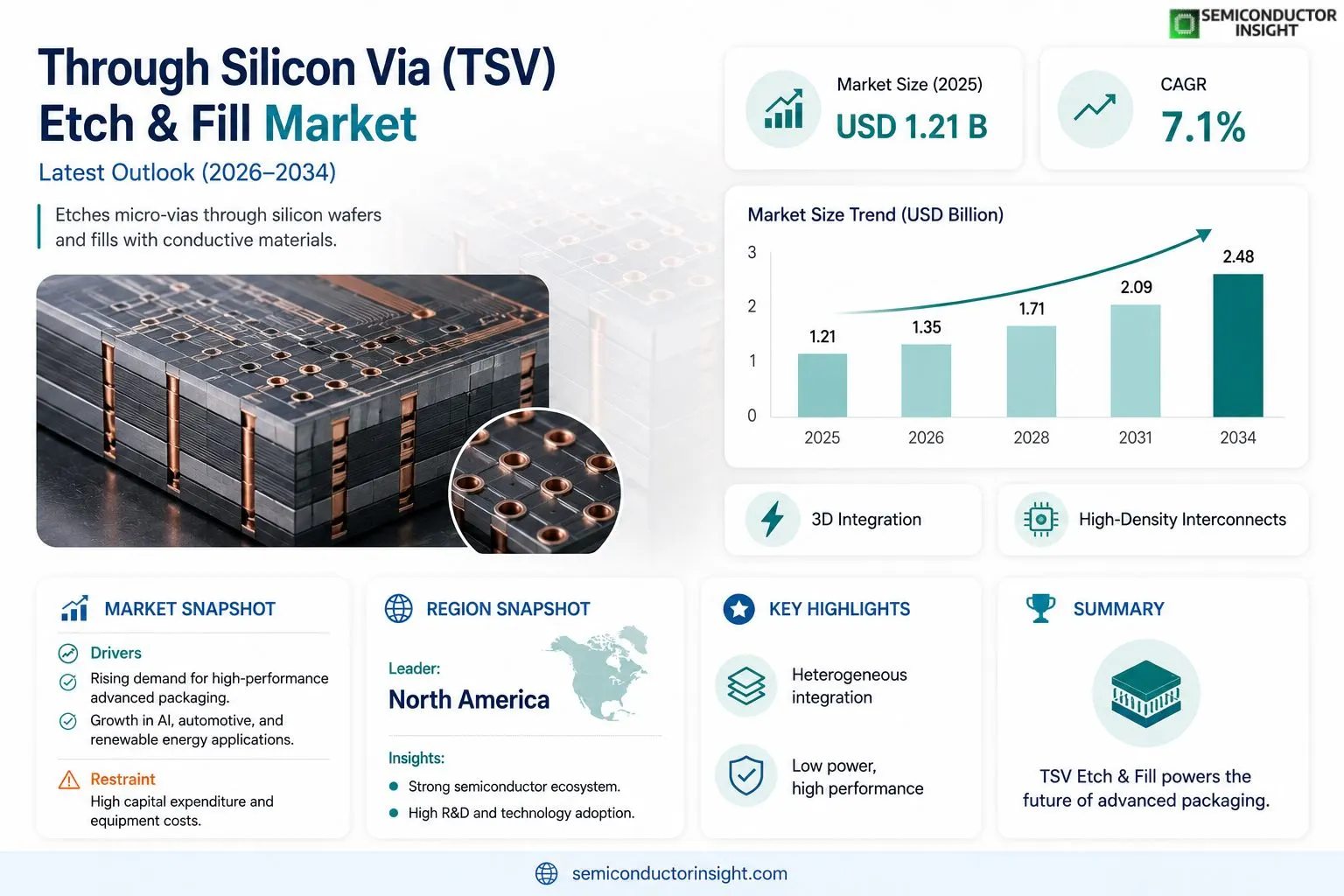
Global TSV Etch & Fill market size was valued at USD 1.21 billion in 2025. The market is projected to grow from USD 1.35 billion in 2026 to USD 2.48 billion by 2034, exhibiting a CAGR of 7.1% during the forecast period.
Through Silicon Via (TSV) Etch & Fill technology enables high‑density vertical interconnections by etching precise micro‑holes through silicon wafers and subsequently filling them with conductive materials such as copper or tungsten. This process is critical for advanced packaging solutions, including heterogeneous integration and three‑dimensional IC stacking.
The market is gaining momentum because semiconductor manufacturers are accelerating adoption of heterogeneous integration to meet demand for higher performance and lower power consumption in AI, automotive, and mobile applications. Furthermore, ongoing investments in advanced lithography and material science are reducing defect rates, while leading vendors are expanding their TSV portfolios through strategic collaborations and technology roadmaps.
MARKET DRIVERS
Increasing Demand for High‑Performance Packaging
Through Silicon Via (TSV) Etch & Fill Market is being propelled by the surge in advanced semiconductor packaging required for AI, 5G, and automotive applications. Manufacturers seek higher interconnect density and lower signal loss, driving adoption of TSV technologies.
Advancements in Etch and Fill Materials
Recent innovations in dielectric and copper fill chemistries have improved yield and reduced cycle time, making TSV Etch & Fill processes more cost‑effective for volume production.
➤ Integration of TSV with heterogeneous integration platforms is unlocking new device form factors and boosting market momentum.
Furthermore, the push for miniaturization in mobile devices is creating a strong incentive for fabless companies to adopt TSV solutions, reinforcing market growth.
MARKET CHALLENGES
Complexity of Process Integration
Integrating TSV Etch & Fill steps with existing front‑end and back‑end flows demands precise thermal budgets and strict contamination control, increasing engineering overhead.
Other Challenges
Yield Management
Maintaining high yield across large wafer volumes remains a critical issue, as defects in etch depth or fill voids can lead to costly rework.
MARKET RESTRAINTS
High Capital Expenditure
Establishing TSV Etch & Fill lines requires significant investment in specialized equipment and cleanroom upgrades, which can deter medium‑size fabs from entering the market.Additionally, the lack of standardized process modules leads to variable cost structures, limiting broader adoption among cost‑sensitive manufacturers.Regulatory scrutiny over material safety, especially for new dielectric compounds, adds compliance costs that can further restrain market expansion.
MARKET OPPORTUNITIES
Emerging Applications in Neuromorphic Computing
Neuromorphic chips require ultra‑dense vertical interconnects, presenting a significant growth avenue for Through Silicon Via (TSV) Etch & Fill Market as designers seek 3‑D integration solutions.Another promising segment is the automotive sensor market, where high‑reliability TSV structures enable compact radar and lidar modules, driving demand for robust etch and fill processes.Finally, collaborations between equipment vendors and foundries to develop modular TSV platforms are expected to lower entry barriers, creating new revenue streams for service providers.
Through Silicon Via (TSV) Etch & Fill Market Trends
Accelerating Adoption of Heterogeneous Integration
The Through Silicon Via (TSV) Etch & Fill process continues to gain traction as semiconductor manufacturers prioritize three‑dimensional (3D) integration to meet escalating performance demands. By precisely etching micro‑holes through silicon wafers and filling them with conductive materials, the technology enables high‑density vertical interconnects that reduce package footprint and signal latency. Recent advances in lithography and process control have improved alignment accuracy, allowing designers to embed TSVs in increasingly complex heterogeneous stacks without compromising yield. This momentum is driven primarily by the need for higher bandwidth and lower power consumption in emerging AI accelerators, advanced driver‑assistance systems (ADAS), and next‑generation mobile platforms.
Other Trends
Materials Innovation Reducing Defect Rates
Innovation in barrier and fill materials is a critical sub‑trend shaping the TSV Etch & Fill landscape. Copper remains the dominant fill material due to its excellent conductivity, yet recent research into tungsten and novel alloy compositions is addressing reliability concerns such as electromigration and thermal expansion mismatch. Simultaneously, low‑k dielectric barriers and plasma‑enhanced deposition techniques are lowering defect densities during the etch phase. These material improvements are supported by collaborative R&D programs among leading foundries and equipment suppliers, resulting in tighter process windows and higher overall throughput.
Expansion into AI, Automotive, and Mobile Applications
Market participants are extending TSV Etch & Fill capabilities to address the specific needs of AI, automotive, and mobile segments. In AI hardware, dense TSV arrays enable multi‑chip module (MCM) configurations that combine logic, memory, and analog blocks within a single package, delivering the computational density required for deep‑learning workloads. Automotive manufacturers are leveraging TSV‑enabled 3D packages to consolidate power management, sensor integration, and safety‑critical functions, thereby meeting stringent reliability and thermal specifications. Mobile device designers benefit from the size reductions and signal integrity improvements offered by TSVs, allowing thinner form factors without sacrificing performance. Strategic alliances between silicon designers and TSV equipment vendors are accelerating product roadmaps, ensuring that the technology remains aligned with the rapid evolution of these high‑growth markets.
COMPETITIVE LANDSCAPE
Key Industry Players
Through Silicon Via (TSV) Etch & Fill Market Competitive Overview
TSV Etch & Fill Market is dominated by a handful of vertically integrated semiconductor manufacturers that control both wafer processing and advanced packaging capabilities. Intel maintains a leading position through its aggressive investment in 3‑D stacking for data‑center and AI workloads, leveraging in‑house TSV expertise to reduce interconnect resistance and improve thermal performance. TSMC and Samsung follow closely, offering TSV‑enabled foundry services that enable customers to adopt heterogeneous integration without building dedicated etch lines. These tier‑one players benefit from scale economies, extensive R&D budgets, and strategic collaborations with equipment suppliers, which together shape the market’s supply‑side dynamics and drive the projected 7.1% CAGR toward 2034.
Beyond the dominant firms, a diverse ecosystem of specialized equipment, materials, and packaging providers fuels innovation in niche segments. Applied Materials and Lam Research supply the critical plasma etch and deposition tools that define TSV hole geometry and fill quality, while Tokyo Electron provides high‑throughput lithography solutions that improve defect yields. Packaging specialists such as ASE Technology, Amkor Technology, and STMicroelectronics integrate TSV processes into advanced‑pack services for automotive, AI, and mobile applications. Regional players including Infineon, NXP, Hitachi High‑Tech, and SPTS Technologies focus on particular material chemistries or wafer‑size niches, creating competitive pressure that encourages continuous technology road‑mapping across the value chain.
List of Key TSV Etch & Fill Companies Profiled
- Intel
- TSMC
- Samsung Electronics
- Applied Materials
- Lam Research
- Tokyo Electron
- ASE Technology Holding
- Amkor Technology
- STMicroelectronics
- Infineon Technologies
- NXP Semiconductors
- Hitachi High‑Tech
- SPTS Technologies
- GlobalFoundries
- IBM
Segment Analysis:
| Segment Category | Sub-Segments | Key Insights |
| By Type |
|
Copper Fill TSV is widely regarded as the leading segment because it offers superior electrical conductivity and thermal performance.
|
| By Application |
|
AI Accelerators dominate the application landscape as designers seek ultra‑high bandwidth pathways for data‑intensive workloads.
|
| By End User |
|
Semiconductor Foundries emerge as the primary end‑user segment, driving demand for robust TSV solutions.
|
| By Technology |
|
Dry Etch Process is considered the leading technology due to its superior control over via geometry and reduced sidewall damage.
|
| By Process Stage |
|
Dielectric Filling stands out as the critical stage because it directly influences electrical reliability and mechanical stability.
|
Regional Analysis: North America
United States
The US boasts a thriving foundry ecosystem, with major players continuously investing in advanced process technologies to accommodate TSV integration. This competitive landscape drives innovation and helps to reduce costs associated with TSV manufacturing.
North America is at the forefront of packaging innovations utilizing TSV technology. Companies are exploring different TSV materials and architectures to improve signal integrity and thermal dissipation in advanced chips.
Key applications driving TSV adoption in the US include high-performance computing, data centers, and automotive electronics, where the demand for increased processing power and connectivity is paramount.
Significant investments are being directed towards TSV research, development, and manufacturing infrastructure in the United States, indicating strong long-term growth potential.
Europe
European markets are witnessing steady growth in Through Silicon Via (TSV) Etch & Fill Market. While not as dominant as North America, the region benefits from a strong foundation in automotive, industrial, and consumer electronics. European manufacturers are increasingly adopting TSV technology to enhance the performance and efficiency of their products. Business strategies in Europe often emphasize collaboration within the European Union to foster innovation and address supply chain concerns. There’s a growing emphasis on sustainable manufacturing practices within the European TSV market.
Asia-Pacific
Asia-Pacific represents a rapidly expanding market for Through Silicon Via (TSV) Etch & Fill. Driven by the immense growth of the electronics manufacturing industry in countries like China, Japan, and South Korea, the demand for advanced packaging solutions is surging. The region is seeing significant investments in TSV infrastructure and a rise in local TSV providers. Business strategies in Asia-Pacific are often characterized by aggressive pricing and a focus on high-volume production. The automotive sector in Asia-Pacific is also a key driver for TSV adoption.
South America
Through Silicon Via (TSV) Etch & Fill Market in South America is currently in its early stages of development. However, with the growing adoption of electronics in various sectors, including telecommunications and industrial automation, the market is expected to witness gradual growth in the coming years. Initial adoption is focused on specific high-end applications. Business strategies in this region are primarily centered around introducing and educating potential customers about the benefits of TSV technology.
Middle East & Africa
The Middle East & Africa region presents a nascent market for Through Silicon Via (TSV) Etch & Fill Market. While the electronics industry is developing, the demand for advanced packaging technologies is still relatively low. However, with increasing investments in infrastructure and technology across the region, there is potential for future growth. Early adoption is likely to be driven by specific niche applications in sectors like aerospace and defense.
Report Scope
This market research report provides a comprehensive analysis of the Through Silicon Via (TSV) Etch & Fill Market , covering the forecast period 2026–2034. It offers detailed insights into market dynamics, technological advancements, competitive landscape, and key trends shaping the industry.
Key focus areas of the report include:
- Market Overview: The report begins with an overview outlining its current market scenario, key growth indicators, and industry transformation drivers. It discusses macroeconomic factors, demand–supply balance, regulatory landscape, and the strategic role of semiconductors in powering advancements across industries such as automotive, telecommunications, consumer electronics, and industrial automation.
- Market Size & Forecast: Historical data and future projections for revenue, unit shipments, and market value across major regions and segments.
- Segmentation Analysis: Detailed breakdown by product type, technology, application, and end-user industry to identify high-growth segments and investment opportunities.
- Regional Insights: Insights into market performance across North America, Europe, Asia-Pacific, Latin America, and the Middle East & Africa, including country-level analysis where relevant.
- Competitive Landscape: Profiles of leading market participants, including their product offerings, R&D focus, manufacturing capacity, pricing strategies, and recent developments such as mergers, acquisitions, and partnerships.
- Technology Trends & Innovation: Assessment of emerging technologies, integration of AI/IoT, semiconductor design trends, fabrication techniques, and evolving industry standards.
- Market Drivers & Restraints: Evaluation of factors driving market growth along with challenges, supply chain constraints, regulatory issues, and market-entry barriers.
- Stakeholder Insights: Insights for component suppliers, OEMs, system integrators, investors, and policymakers regarding the evolving ecosystem and strategic opportunities.
Primary and secondary research methods are employed, including interviews with industry experts, data from verified sources, and real-time market intelligence to ensure the accuracy and reliability of the insights presented.
FREQUENTLY ASKED QUESTIONS:
What is the current market size of Through Silicon Via (TSV) Etch & Fill Market?
-> Through Silicon Via (TSV) Etch & Fill Market was valued at USD 1.21 billion in 2025 and is expected to reach USD 2.48 billion by 2034. The market is projected to grow at a CAGR of 7.1% during the forecast period.
Which key companies operate in Through Silicon Via (TSV) Etch & Fill Market?
-> Key players include TSMC, Intel, Samsung, Applied Materials, ASML, GlobalFoundries, among others.
What are the key growth drivers?
-> Key growth drivers include heterogeneous integration, AI-driven applications, automotive electronics, and mobile device demand.
Which region dominates the market?
-> Asia-Pacific is expected to be the fastest‑growing region, while North America remains a significant market.
What are the emerging trends?
-> Emerging trends include 3D IC stacking, advanced lithography techniques, and the use of copper and tungsten conductive fillings.

Get Sample Report PDF for Exclusive Insights
Report Sample Includes
- Table of Contents
- List of Tables & Figures
- Charts, Research Methodology, and more...
 Download Sample Report PDF


