Silicon-on-Sapphire Wafers Market Insights
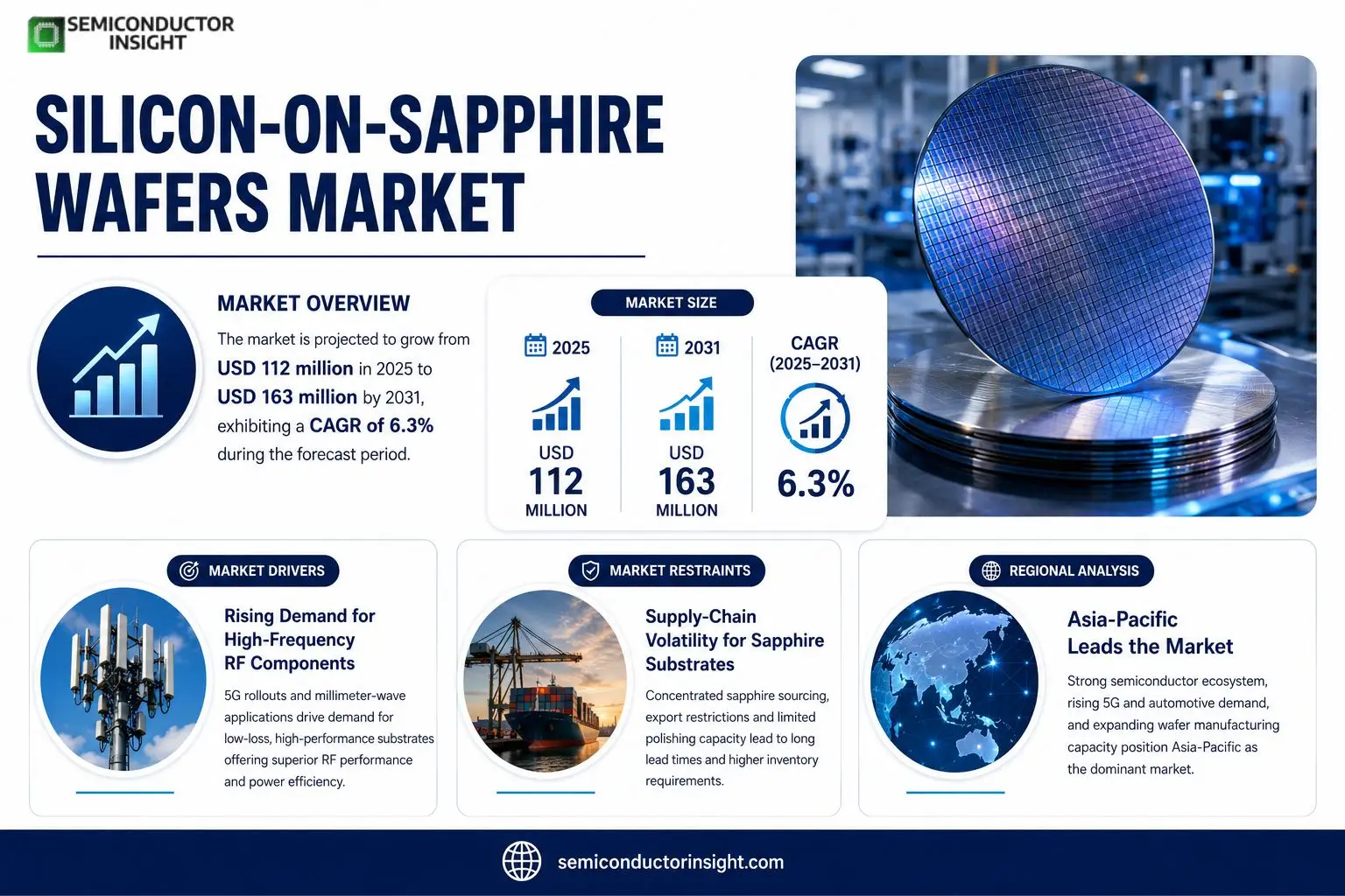
Silicon-on-Sapphire Wafers Market size was valued at USD 108 million in 2024. The market is projected to grow from USD 112 million in 2025 to USD 163 million by 2031, exhibiting a CAGR of 6.3% during the forecast period.
Silicon‑on‑Sapphire is a hetero‑epitaxial process employed for integrated‑circuit manufacturing. Wafer diameters span from 3 inches up to 200 mm, and they are commonly offered in small‑lot sizes that suit research and development applications.The sector is advancing because semiconductor designers value the high‑frequency performance and radiation tolerance that sapphire substrates provide. Recent activity includes Epiel’s capacity expansion announced early 2024, Soitec’s collaboration with Cryscore on low‑defect production techniques, and ongoing portfolio enhancements by these leading suppliers.
MARKET DRIVERS
Rising Demand for High‑Frequency RF Components
Silicon-on-Sapphire Wafers Market is being propelled by telecom operators’ rollout of millimeter‑wave antennas for 5G. Sapphire’s superior dielectric loss makes it ideal for front‑end modules that must operate above 30 GHz while maintaining low insertion loss. Manufacturers that can integrate silicon circuitry directly on sapphire are gaining a pricing premium because their products enable smaller, lighter base stations that meet stringent power‑efficiency targets.
Advancements in Integrated Photonics
Parallel to RF growth, photonic‑engineered devices are exploiting sapphire’s optical transparency and thermal stability. Recent wafer‑scale demonstrations of silicon‑on‑sapphire waveguides show propagation losses under 0.5 dB/cm, a benchmark that positions the platform for data‑center interconnects and LIDAR. Companies that leverage this capability can differentiate their portfolios from conventional silicon‑on‑insulator lanes, reducing the need for separate substrate inventories.
➤ By aligning wafer design with both RF and photonic specifications, suppliers can capture cross‑segment revenue that would otherwise remain fragmented.
In practice, the convergence of these two technology streams is encouraging OEMs to consolidate their supplier base. This consolidation reduces procurement overhead and creates a feedback loop where higher volume orders lower per‑unit costs, further stimulating market adoption.
MARKET CHALLENGES
Cost Sensitivity in High‑Volume Production
Although sapphire offers unrivaled performance, its raw material cost remains 30‑40 % higher than standard silicon substrates. For commodity‑grade devices, this premium can erode margins, especially when buyers apply aggressive price‑negotiation tactics. End‑users therefore scrutinize each design iteration for cost‑saving opportunities, often favoring hybrid approaches that combine sapphire only where performance gains justify the expense.
Other Challenges
Yield Management
Achieving consistent crystalline quality across 8‑inch wafers is technically demanding. Defect densities above 1 cm⁻² translate into chip‑level yield losses that inflate overall project budgets. Suppliers are investing in epitaxial growth controls, yet the learning curve continues to affect short‑term supply reliability.
MARKET RESTRAINTS
Supply‑Chain Volatility for Sapphire Substrates
Sapphire mining is concentrated in a handful of regions, making the upstream supply susceptible to geopolitical tensions and logistics bottlenecks. Recent export restrictions in key producing countries have introduced lead‑times that can exceed eight weeks for premium‑grade boules, compelling manufacturers to hold larger safety stocks and consequently tie up capital.Moreover, the limited number of polishing facilities capable of delivering sub‑nanometer surface flatness constrains the pace at which new capacity can be brought online. This bottleneck curtails the ability of Silicon-on-Sapphire Wafers Market to respond swiftly to sudden demand spikes in emerging applications such as satellite‑based communications.In the longer term, the scarcity of skilled labor for crystal growth and wafer processing adds another layer of operational risk. Companies that fail to secure reliable talent pipelines may experience production slowdowns, further tightening market supply.
MARKET OPPORTUNITIES
Emerging Applications in 5G and Space
Space‑grade transceivers and ground‑station modules for 5G are increasingly demanding substrates that can endure radiation while maintaining low dielectric loss. Sapphire’s inherent radiation hardness makes it a natural fit, and early adopters are reporting up to 20 % improvements in signal integrity compared with traditional silicon platforms.Additionally, the advent of quantum‑sensing devices that rely on low‑noise microwave resonators presents a niche yet high‑value segment. Silicon‑on‑sapphire’s ability to host superconducting circuits with minimal parasitic coupling is attracting interest from defense contractors and research labs, opening a premium revenue stream for specialized wafer providers.Finally, strategic partnerships between fabless designers and specialty wafer foundries are emerging to co‑develop application‑specific processes. Such collaborations can accelerate time‑to‑market for next‑generation products, allowing participants to capture market share before broader industry adoption becomes mainstream.
Silicon-on-Sapphire Wafers Market Trends
Increasing Deployment in RF and Sensor Modules
Silicon-on-Sapphire Wafers Market is experiencing a noticeable uptick as designers of radio‑frequency (RF) front‑ends and high‑precision sensors seek the superior dielectric isolation that sapphire substrates provide. Recent product launches in 5G smartphones and automotive lidar systems have highlighted the material’s low parasitic capacitance, which translates into better signal integrity at millimeter‑wave frequencies. This technical advantage has prompted several fabless firms to prioritize sapphire‑on‑silicon platforms for prototype runs, thereby generating a modest but persistent demand pull across the research‑development segment.
Other Trends
Shift Toward Smaller Wafer Diameters for R&D
Manufacturers are increasingly offering 3‑inch and 4‑inch sapphire wafers to accommodate niche applications that do not require high‑volume production. The smaller lot sizes enable universities and start‑ups to experiment with heterogeneous integration without incurring the overhead associated with larger 200‑mm runs. As a result, the supply chain has adjusted by expanding low‑volume tooling, which in turn reduces lead times for experimental batches and encourages faster iteration cycles.
Geographic Realignment of Supply Chains
While Asia‑Pacific remains the dominant region for semiconductor output, Silicon-on-Sapphire Wafers Market is seeing a subtle redistribution of sourcing strategies. Heightened geopolitical scrutiny and recent capacity constraints have motivated North American and European OEMs to diversify away from single‑source suppliers. Companies based in the United States and Germany are now securing shelf stock of sapphire wafers to mitigate the risk of disruption, a move that also supports local job creation in specialty crystal growth facilities. This realignment not only cushions end‑users against supply shocks but also opens avenues for regional pricing differentiation, prompting competitors to revisit their distribution models.
COMPETITIVE LANDSCAPE
Key Industry Players
Silicon-on-Sapphire Wafer Market: Competitive Positioning and Strategic Outlook
Soitec commands the largest share of the silicon‑on‑sapphire wafer market, leveraging its deep expertise in hetero‑epitaxial processes and a broad portfolio that spans 3‑inch to 200‑mm diameters. The French firm’s vertically integrated modelcovering crystal growth, wafer polishing, and thin‑film depositionallows it to capture premium pricing for high‑performance substrates used in RF, photonics and aerospace sensors. Soitec’s recent expansion of a 150‑mm production line in France reflects a strategic push to serve larger‑scale volume customers while maintaining the low‑lot flexibility prized by research labs. Competitors such as Cryscore and Epitel have carved out niche positions by focusing on ultra‑thin sapphire substrates for MEMS and pressure‑sensor applications, where cost sensitivity and fast turnaround outweigh economies of scale. Their agility in offering custom orientations and rapid prototyping reinforces a fragmented market structure in which a handful of large suppliers coexist with specialized boutique firms catering to emerging sensor and quantum‑device segments.Beyond the incumbents, a cohort of Asian manufacturersWafers, Shin‑Etsu Hand, Sumitomo, and United Siliconhas accelerated capacity investment in response to rising demand from automotive radar and 5G infrastructure. These companies benefit from proximity to major semiconductor fabs, enabling tighter supply chain coordination and lower freight expenses. The entry of United Silicon into the 100‑mm sapphire wafer space illustrates how rising sensor adoption is diluting the historical dominance of analog‑focused players. Meanwhile, firms such as NIPPON and AIXTRON, though primarily known for equipment, are influencing the competitive dynamics by offering advanced crystal‑growth tools that lower entry barriers for new entrants. The resulting landscape is a mix of scale‑driven price competition, technology‑centric differentiation, and strategic partnerships aimed at unlocking new applications in harsh‑environment electronics.
List of Key Silicon-on-Sapphire Companies Profiled
- Soitec
- Wafers
- Cryscore
- Shin-Etsu Hand
- Epitel
- Sumitomo
- United Silicon
- NIPPON
- IQE
- AIXTRON
- Skyworks Solutions
- Qorvo
- ROHM Semiconductor
Segment Analysis:
| Segment Category | Sub-Segments | Key Insights |
| By Type |
|
150 mm wafers are emerging as the preferred type for most research‑driven projects.
|
| By Application |
|
RF components dominate application discussions.
|
| By End User |
|
Defense and aerospace remain the leading end‑user segment.
|
| By Process Technology |
|
Hetero‑epitaxial growth is the dominant process route.
|
| By Market Role |
|
Research & development drives the current market dynamics.
|
Regional Analysis: Silicon-on-Sapphire Wafers Market
Asia‑Pacific
China leverages its extensive fab capacity to offset supply constraints elsewhere, integrating sapphire growth lines with mature silicon processing. The strategic focus on vertical integration permits tighter control over wafer thickness and defect density, delivering products that meet the exacting specifications of advanced RF modules.
Japanese research institutes continue to pioneer epitaxial techniques that improve crystalline uniformity. Their collaborations with equipment vendors accelerate the adoption of low‑temperature deposition methods, which in turn lowers energy consumption across the supply chain.
Korean automakers are embedding Silicon‑on‑Sapphire wafers into next‑generation radar sensors, valuing the material’s resilience to temperature swings. This partnership drives bespoke wafer sizes that align with compact module designs, reinforcing regional demand.
Taiwan’s ecosystem benefits from rapid scaling of wafer handling equipment, allowing quick pivots between volume orders and niche prototypes. The nimble logistics network shortens lead times for multinational chip designers seeking flexible sourcing options.
North America
In North America, the Silicon‑on‑Sapphire wafers market is anchored by a handful of legacy manufacturers that cater to defense and aerospace clients requiring high‑performance optics. The region’s emphasis on stringent qualification standards sustains a premium pricing tier, compelling suppliers to differentiate through superior defect management. Concurrently, venture capital is channeling funds into niche start‑ups exploring photonic integration, which could broaden the addressable market beyond traditional radar applications. However, the reliance on imported sapphire substrates introduces a vulnerability that many firms are attempting to mitigate through strategic partnerships with Asian growers.
Europe
European stakeholders view Silicon‑on‑Sapphire wafers as a critical component for emerging quantum communication prototypes and satellite‑grade RF hardware. Policy frameworks that prioritize sovereign technology development encourage local fabs to adopt sapphire substrates despite higher material costs. Collaboration between research consortia and equipment manufacturers accelerates the rollout of low‑defect epitaxy, supporting countries that aim to retain a competitive edge in high‑frequency communications. The market remains modest in volume but benefits from strong intellectual property generation that fuels downstream innovation.
South America
South American interest in Silicon‑on‑Sapphire wafers is currently driven by telecom operators upgrading to 5G infrastructure. While local fabrication capabilities are limited, regional distributors are establishing tighter links with Asian suppliers to guarantee a steady flow of wafers for base‑station modules. Governments are beginning to outline incentives for domestic assembly plants, hinting at a gradual shift from pure import reliance toward a more localized value chain.
Middle East & Africa
The Middle East & Africa region exhibits nascent demand for Silicon‑on‑Sapphire wafers, primarily within defense procurement programmes that value the material’s thermal robustness. Several Gulf states are investing in research parks that partner with Asian suppliers to explore high‑frequency radar applications for maritime surveillance. In Africa, limited industrial activity keeps market size modest, yet emerging satellite initiatives present a potential catalyst for future adoption of sapphire‑based photonic components.
Report Scope
This market research report provides a comprehensive analysis of the Silicon-on-Sapphire Wafers Market , covering the forecast period 2026–2034. It offers detailed insights into market dynamics, technological advancements, competitive landscape, and key trends shaping the industry.
Key focus areas of the report include:
- Market Overview: The report begins with an overview outlining its current market scenario, key growth indicators, and industry transformation drivers. It discusses macroeconomic factors, demand–supply balance, regulatory landscape, and the strategic role of semiconductors in powering advancements across industries such as automotive, telecommunications, consumer electronics, and industrial automation.
- Market Size & Forecast: Historical data and future projections for revenue, unit shipments, and market value across major regions and segments.
- Segmentation Analysis: Detailed breakdown by product type, technology, application, and end-user industry to identify high-growth segments and investment opportunities.
- Regional Insights: Insights into market performance across North America, Europe, Asia-Pacific, Latin America, and the Middle East & Africa, including country-level analysis where relevant.
- Competitive Landscape: Profiles of leading market participants, including their product offerings, R&D focus, manufacturing capacity, pricing strategies, and recent developments such as mergers, acquisitions, and partnerships.
- Technology Trends & Innovation: Assessment of emerging technologies, integration of AI/IoT, semiconductor design trends, fabrication techniques, and evolving industry standards.
- Market Drivers & Restraints: Evaluation of factors driving market growth along with challenges, supply chain constraints, regulatory issues, and market-entry barriers.
- Stakeholder Insights: Insights for component suppliers, OEMs, system integrators, investors, and policymakers regarding the evolving ecosystem and strategic opportunities.
Primary and secondary research methods are employed, including interviews with industry experts, data from verified sources, and real-time market intelligence to ensure the accuracy and reliability of the insights presented.
FREQUENTLY ASKED QUESTIONS:
What is the current market size of Silicon-on-Sapphire Wafers Market?
-> Silicon-on-Sapphire Wafers Market was valued at USD 108 million in 2024 and is projected to reach USD 163 million by 2031, growing at a CAGR of 6.3% during the forecast period.
Which key companies operate in Silicon-on-Sapphire Wafers Market?
-> Key players include Epiel, Cryscore, Soitec, among others.
What are the key growth drivers?
-> Key growth drivers include increasing demand for advanced integrated circuits, expanding applications in pressure sensors and ICs, and the availability of small‑lot wafer sizes that support research and development activities.
Which region dominates the market?
-> Asia-Pacific remains the largest region by revenue, although it experienced a slight decline of 2.0 % in 2022, while the Americas showed strong growth with a 17.0 % increase in sales.
What are the emerging trends?
-> Emerging trends include the development of larger wafer diameters (up to 200 mm), diversification into pressure‑sensor and IC applications, and heightened focus on hetero‑epitaxial processes for next‑generation semiconductor devices.
Get Sample Report PDF for Exclusive Insights
Report Sample Includes
- Table of Contents
- List of Tables & Figures
- Charts, Research Methodology, and more...
 Download Sample Report PDF