Silicon Nitride Film Window Market Insights
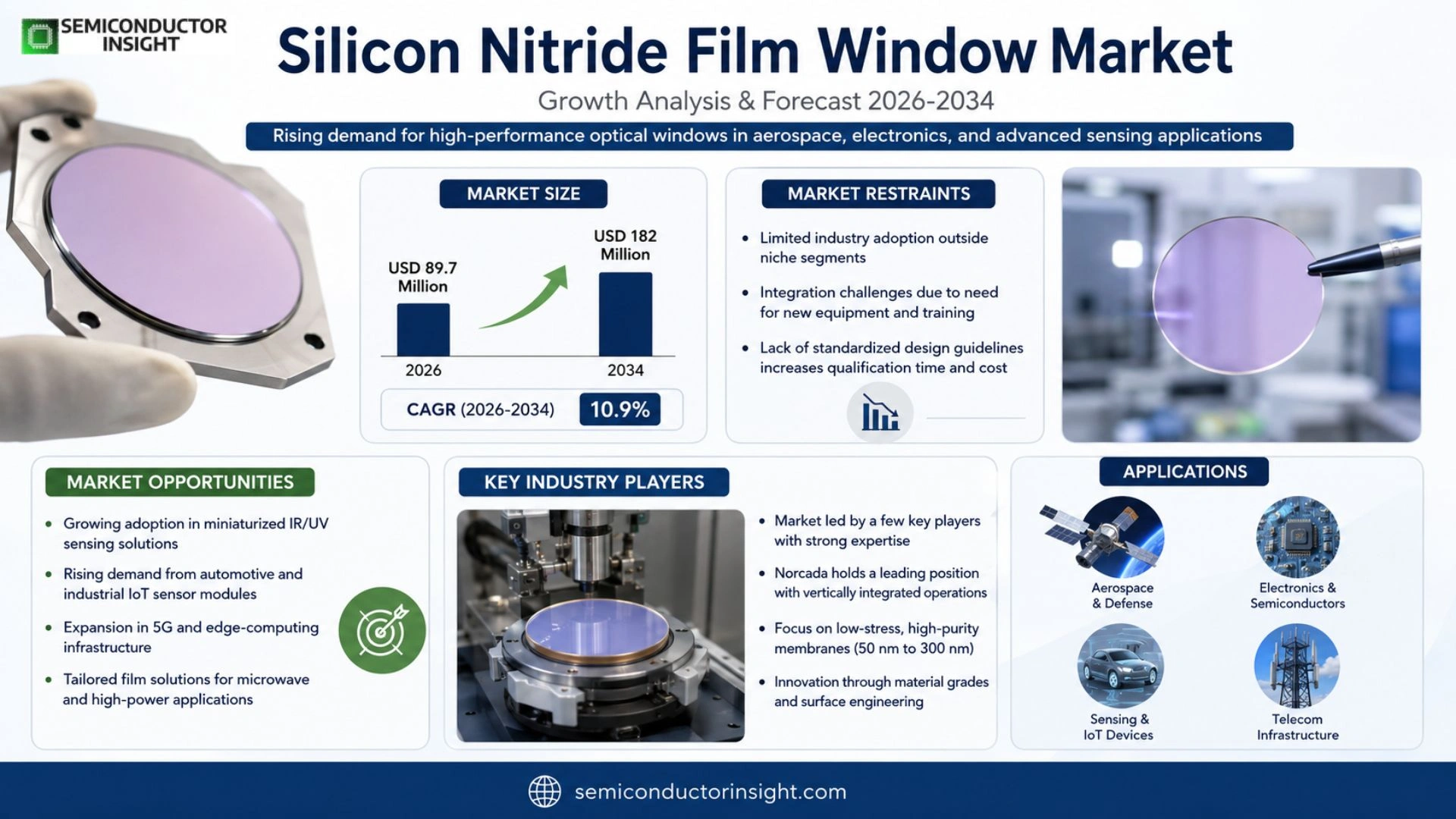
Global Silicon Nitride Film Window market is projected to grow from USD 89.7 million in 2026 to USD 182 million by 2034, exhibiting a CAGR of 10.9% during the forecast period.
Silicon Nitride Film Window refers to ultra‑thin Si₃N₄ membranes that serve as support windows for high‑resolution analytical techniques. These films are integral to Transmission Electron Microscopy (TEM) – especially low‑stress Si₃N₄ TEM grids – and are also employed in X‑Ray microscopy where their mechanical stability and low background scattering enhance image quality.
The expansion of this niche market stems from rising demand for advanced microscopy in semiconductor failure analysis, materials science research, and biomedical imaging. Manufacturers such as Norcada, Ted Pella, YW MEMS and Beike 2D Materials have broadened their portfolios to address specific thickness requirements (e.g., 50 nm, 100 nm) while improving film uniformity. Concurrently, increasing investment in R&D across North America and Asia fuels adoption of silicon nitride windows for next‑generation analytical platforms.
MARKET DRIVERS
Rising Demand in High‑Temperature Environments
Silicon Nitride Film Window Market is benefitting from a surge in applications where thermal resilience is non‑negotiable. Aerospace engine components, turbo‑charged automotive exhaust systems, and next‑generation power electronics all require transparent barriers that can survive temperatures above 800 °C without compromising optical clarity. Manufacturers are therefore prioritizing silicon nitride films to replace conventional glass, a shift that translates into steadier order books for specialty coating providers.
Advances in Deposition and Patterning Technologies
Recent breakthroughs in plasma‑enhanced chemical vapor deposition (PECVD) and atomic layer deposition (ALD) have lowered defect densities and improved uniformity across large substrates. These process gains reduce scrap rates and enable thinner windows that still meet mechanical strength criteria, opening up cost‑effective pathways for mass‑market adoption. Companies that have integrated these tools are reporting shorter lead times and higher yields, which fuels confidence across the supply chain.
➤ Industry insiders note that every 10 % improvement in deposition throughput can unlock a comparable increase in market penetration for silicon nitride windows.
Overall, the combination of stringent performance requirements and more efficient manufacturing is creating a virtuous cycle: higher demand justifies investment in tooling, and the resulting economies of scale make Silicon Nitride Film Window Market increasingly attractive to new entrants.
MARKET CHALLENGES
Cost Competitiveness with Conventional Materials
While silicon nitride offers unmatched thermal and mechanical properties, its raw material cost and processing expense remain higher than those of soda‑lime glass or polymeric alternatives. End‑users often face internal budgeting pressures that force a trade‑off between performance and price, limiting the willingness to adopt premium windows for low‑margin products. This price sensitivity dampens volume growth in sectors where cost is the primary purchase driver.
Other Challenges
Supply Chain Constraints
The specialty gases and high‑purity silicon sources required for thin‑film deposition are sourced from a narrow supplier base. Recent geopolitical tensions and logistical bottlenecks have sporadically disrupted deliveries, prompting manufacturers to hold larger safety stocks and thereby increasing overall inventory costs.
MARKET RESTRAINTS
Limited Industry Adoption Outside Niche Segments
Beyond aerospace and high‑performance electronics, many traditional optics manufacturers remain hesitant to redesign product lines around silicon nitride films. The perceived integration risk, requiring new equipment, staff training, and redesign of assembly fixtures, creates a barrier that slows diffusion into broader markets such as consumer electronics or architectural glazing.
The inertia is compounded by the lack of standardized design guidelines for silicon nitride windows. Without widely accepted specifications, engineering teams must allocate additional resources to perform custom qualification testing, which discourages speculative adoption.
MARKET OPPORTUNITIES
Emerging Sensing Solutions
Miniaturized infrared and ultraviolet sensors increasingly rely on windows that transmit specific wavelengths while blocking harsh environmental factors. Silicon nitride’s selective transparency and abrasion resistance make it an ideal candidate, positioning Silicon Nitride Film Window Market to capture a growing share of next‑generation sensor modules used in autonomous vehicles and industrial IoT devices.
Another promising avenue lies in the rollout of 5G and edge‑computing infrastructure, where high‑power microwave components benefit from robust protective windows. Companies that can tailor film thickness to balance insertion loss with mechanical shielding stand to secure contracts with telecommunications equipment makers.
Finally, defense procurement programs are earmarking budgets for durable optical enclosures capable of withstanding shock and temperature extremes. Early engagement with defense contractors could translate into long‑term supply agreements, providing a stable revenue stream for firms that have mastered high‑reliability silicon nitride production.
Silicon Nitride Film Window Market Trends
Growing Adoption in Advanced Microscopy
Silicon Nitride Film Window has become a preferred substrate for transmission electron microscopy (TEM) and X‑ray microscopy because its low‑stress architecture preserves specimen integrity while delivering high‑resolution imaging. Laboratories focused on nanostructure analysis are replacing traditional carbon films with silicon nitride alternatives, citing superior mechanical stability and reduced background scattering. This shift is not merely technical; it translates into faster throughput for research projects, allowing service providers to offer premium analysis packages that command higher price points. Consequently, demand for ultra‑thin (50 nm) and moderately thin (100–200 nm) windows is outpacing growth in larger‑thickness segments, steering supplier inventories toward more refined production lines.
Other Trends
Regional Shifts Toward Asian Production
China’s expanding semiconductor ecosystem is fostering a cluster of silicon nitride film manufacturers that benefit from localized supply chains and government incentives for high‑tech materials. While the United States still hosts several legacy producers, cost differentials and the rapid scaling of Chinese fabs are prompting some U.S. customers to source components from Asian vendors. This geographic rebalancing is prompting incumbents to consider joint ventures or capacity expansions in the Asia‑Pacific to retain market share and meet tighter lead‑time expectations from downstream users.
Material Engineering Innovations
Recent advances in plasma‑enhanced chemical vapor deposition (PECVD) have enabled tighter control over film stress and thickness uniformity, opening opportunities for custom‑specification windows tailored to niche applications such as cryo‑TEM and in‑situ X‑ray spectroscopy. Leading players like Norcada and Ted Pella are investing in R&D pipelines that integrate nanofabrication techniques with silicon nitride coatings, aiming to reduce defect rates and improve batch yields. For end‑users, these innovations mean more reliable performance and lower total cost of ownership, which in turn fuels a virtuous cycle of adoption across academic, industrial, and defense research sectors. The overall trajectory suggests that Silicon Nitride Film Window Market will continue to be shaped by technology‑driven differentiation rather than price competition alone.
COMPETITIVE LANDSCAPE
Key Industry Players
Competitive Dynamics of Silicon Nitride Film Window Suppliers
Silicon Nitride Film Window market is anchored by a handful of firms that control the bulk of high‑purity membrane production for transmission electron microscopy and X‑ray applications. Norcada, with its legacy of precision silicon‑based components, commands the largest share by leveraging a vertically integrated supply chain that spans substrate preparation, thin‑film deposition, and post‑fabrication testing. Its ability to offer low‑stress membranes across the 50 nm to 300 nm range has made it a preferred source for research institutions that demand reproducible performance. The concentration around a core group of providers forces smaller entrants to differentiate through niche material grades or specialized surface treatments, reinforcing a market structure that balances scale economies with targeted innovation.
Beyond the dominant tier, a diverse set of specialists broadens the competitive field. Ted Pella, known for its microscopy consumables, supplies pre‑mounted windows that appeal to laboratories seeking turnkey solutions. YW MEMS and Beike 2D Materials have accelerated development of ultra‑thin, high‑strength films tailored for next‑generation X‑ray microscopy, positioning themselves as technology challengers. Regional manufacturers in China, Japan and South Korea are expanding capacity to meet domestic demand, often competing on price while investing in incremental performance improvements. These players collectively enrich the supplier ecosystem, providing customers with alternatives that span price points, customization options, and geographic proximity.
List of Key Silicon Nitride Film Window Companies Profiled
- Norcada
- Ted Pella
- YW MEMS
- Beike 2D Materials
- Nanofabrication Ltd
- Advanced NanoTech
- China National Thin Film
- Micron Advanced Materials
- NanoView Instruments
- Silicon Power Technologies
- UltraThin Membranes Inc.
- Precision Nanostructures Co.
Segment Analysis:
| Segment Category | Sub-Segments | Key Insights |
| By Type |
|
Ultra‑Thin (50nm)
|
| By Application |
|
Transmission Electron Microscopy (TEM)
|
| By End User |
|
Research Laboratories
|
| By Thickness |
|
Ultra‑Thin
|
| By Functional Requirement |
|
Low‑Stress
|
Regional Analysis: Silicon Nitride Film Window Market
Asia‑Pacific
Leading fabs are upgrading deposition chambers to accommodate larger wafer diameters, thereby improving throughput without sacrificing film integrity. This shift reflects a strategic move to meet rising demand from both consumer electronics and automotive optics, while preserving the precise stress profiles required for high‑performance windows.
Regional suppliers have diversified raw‑material sources, mitigating single‑point failures. Collaborative inventory management platforms enable real‑time visibility across the value chain, ensuring that silicon nitride precursors reach end‑users promptly even during logistical disruptions.
Environmental standards increasingly incentivise low‑emission processes. Companies adopting plasma‑based deposition gain compliance credits, positioning themselves favorably with government bodies that prioritize sustainable manufacturing practices.
Beyond traditional optics, the film is finding roles in quantum‑dot displays and high‑temperature sensor housings. These niche uses demand exceptional thermal stability, prompting vendors to tailor nitride formulations for specialized performance envelopes.
North America
The United States continues to drive innovation in Silicon Nitride Film Window Market through aggressive R&D spending in advanced packaging and defense‑related optics. Research institutions collaborate with equipment makers to push the envelope on film thickness control, fostering a pipeline of next‑generation photonic devices. While cost pressures remain, the region offsets them with premium pricing justified by superior reliability in aerospace and high‑frequency communications applications. Companies that align product roadmaps with governmental procurement cycles stand to benefit from stable demand.
Europe
European manufacturers leverage stringent quality standards to differentiate their silicon nitride offerings, especially in automotive lighting and industrial laser systems. The EU’s emphasis on circular‑economy principles encourages recyclability of deposition equipment, prompting firms to design modular solutions that extend service life. Collaborative projects funded by Horizon initiatives accelerate the transfer of laboratory breakthroughs into scalable processes, reinforcing the continent’s reputation for precision engineering.
South America
In South America, emerging consumer‑electronics assemblers are beginning to integrate silicon nitride film windows into mid‑range smartphones and IoT devices. Local cost advantages attract multinational suppliers seeking to establish footholds without the expense of high‑volume Asian production. The market is still maturing, but early adopters benefit from relatively low entry barriers and a growing skilled labor pool trained in thin‑film technologies.
Middle East & Africa
Investment in telecom infrastructure across the Middle East and select African nations is sparking interest in silicon nitride film windows for ruggedized antenna modules. Government‑driven broadband expansion programs create a steady demand curve, encouraging regional distributors to stock a broader portfolio of high‑performance coatings. Partnerships with Asian manufacturers enable technology transfer, allowing local firms to offer competitive lead times while adhering to international performance benchmarks.
Report Scope
This market research report provides a comprehensive analysis of the Silicon Nitride Film Window Market , covering the forecast period 2026–2034. It offers detailed insights into market dynamics, technological advancements, competitive landscape, and key trends shaping the industry.
Key focus areas of the report include:
- Market Overview: The report begins with an overview outlining its current market scenario, key growth indicators, and industry transformation drivers. It discusses macroeconomic factors, demand–supply balance, regulatory landscape, and the strategic role of semiconductors in powering advancements across industries such as automotive, telecommunications, consumer electronics, and industrial automation.
- Market Size & Forecast: Historical data and future projections for revenue, unit shipments, and market value across major regions and segments.
- Segmentation Analysis: Detailed breakdown by product type, technology, application, and end-user industry to identify high-growth segments and investment opportunities.
- Regional Insights: Insights into market performance across North America, Europe, Asia-Pacific, Latin America, and the Middle East & Africa, including country-level analysis where relevant.
- Competitive Landscape: Profiles of leading market participants, including their product offerings, R&D focus, manufacturing capacity, pricing strategies, and recent developments such as mergers, acquisitions, and partnerships.
- Technology Trends & Innovation: Assessment of emerging technologies, integration of AI/IoT, semiconductor design trends, fabrication techniques, and evolving industry standards.
- Market Drivers & Restraints: Evaluation of factors driving market growth along with challenges, supply chain constraints, regulatory issues, and market-entry barriers.
- Stakeholder Insights: Insights for component suppliers, OEMs, system integrators, investors, and policymakers regarding the evolving ecosystem and strategic opportunities.
Primary and secondary research methods are employed, including interviews with industry experts, data from verified sources, and real-time market intelligence to ensure the accuracy and reliability of the insights presented.
FREQUENTLY ASKED QUESTIONS:
What is the current market size of Silicon Nitride Film Window Market?
-> Silicon Nitride Film Window market is projected to grow from USD 89.7 million in 2026 to USD 182 million by 2034, exhibiting a CAGR of 10.9%
Which key companies operate in Silicon Nitride Film Window Market?
-> Key players include Norcada, Ted Pella, YW MEMS, Beike 2D materials, among others.
What are the key growth drivers?
-> Key growth drivers include rising demand for Transmission Electron Microscopy (TEM) grids, low‑stress silicon nitride films, and expanding applications in X‑Ray microscopy.
Which region dominates the market?
-> North America (United States) and Asia (China) are the largest regional markets, with strong adoption in the United States and rapid growth observed in China.
What are the emerging trends?
-> Emerging trends include development of low‑stress TEM grids, integration of silicon nitride films in X‑Ray microscopy, and advanced thin‑film manufacturing techniques.

Get Sample Report PDF for Exclusive Insights
Report Sample Includes
- Table of Contents
- List of Tables & Figures
- Charts, Research Methodology, and more...
 Download Sample Report PDF