Semiconductor X-ray Diffractometers Market Insights
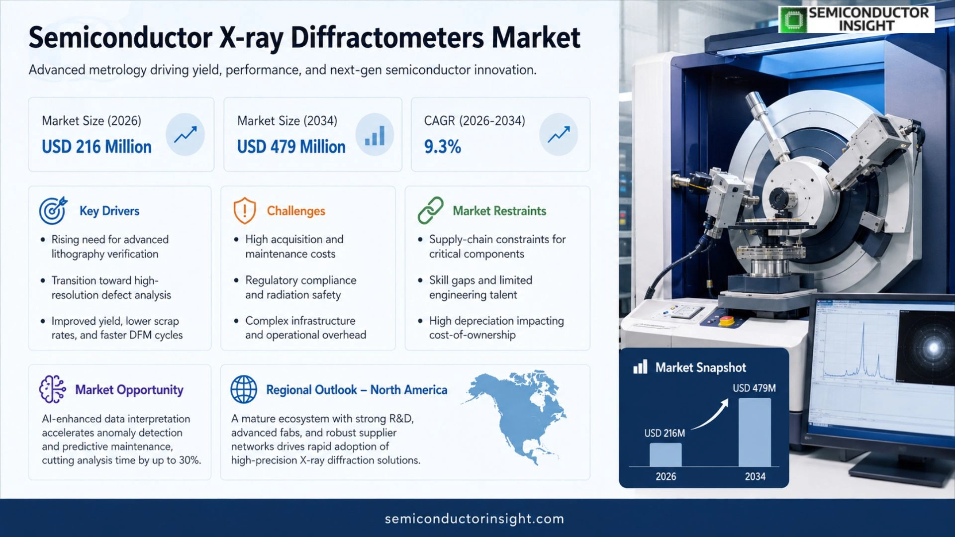
Global Semiconductor X-ray Diffractometers market size was valued at USD 216 million in 2025 and will grow to USD 479 million by 2034, exhibiting a CAGR of 9.3% during the forecast period.
X‑ray diffraction (XRD) remains one of the most reliable non‑destructive techniques for characterising matter ranging from fluids and powders to crystalline wafers. In semiconductor manufacturing, high‑resolution XRD reveals layer parameters such as composition, thickness, roughness and density of thin‑film structures, enabling tighter process control and yield improvement.
The market’s expansion is underpinned by rising investment in advanced node fabrication and increased demand for research‑grade analytical tools in academia and R&D labs. Recent activity includes Malvern Panalytical’s launch of an upgraded high‑resolution diffractometer platform in late 2023, Bruker’s introduction of a compact low‑resolution model aimed at cost‑sensitive fabs, and Rigaku’s partnership with a major foundry to integrate inline XRD monitoring on production lines. Thermo Fisher and Dezisemi continue to broaden their portfolios through software upgrades that enhance data analytics capabilities.
MARKET DRIVERS
Rising need for advanced lithography verification
Semiconductor X-ray Diffractometers Market is being propelled by manufacturers’ push to validate sub‑10 nm pattern fidelity. As node dimensions shrink, traditional optical metrology loses resolution, compelling fabs to adopt X‑ray diffraction techniques that can discern lattice‑scale variations. This shift not only safeguards yield but also shortens cycle time for design‑for‑manufacturing (DFM) loops.
Transition toward high‑resolution defect analysis
Customers are increasingly requiring instruments capable of detecting dislocation densities below 10⁴ cm⁻². Modern diffractometers now combine micro‑focused beams with fast area detectors, delivering sub‑picometer precision. The ability to spot crystalline defects early translates directly into lower scrap rates and higher equipment utilization, making the technology a strategic asset for fabs targeting >70 % production efficiency.
➤ “Investments in next‑generation X‑ray diffraction are delivering a measurable 5‑point improvement in wafer‑level defect yield.”
Beyond yield, the technology supports material‑process innovation, especially for strained‑silicon and germanium channels. By providing real‑time feedback on epitaxial strain, diffractometers enable design teams to push performance envelopes while maintaining reliability, thereby reinforcing the market’s growth trajectory.
MARKET CHALLENGES
High acquisition and maintenance costs
State‑of‑the‑art X‑ray diffractometers command price tags ranging from $800 k to $2 M, and annual service contracts can exceed 10 % of the purchase price. For midsize fabs, such capital intensity strains balance‑sheet flexibility, prompting hesitation even when the analytical benefits are clear.
Other Challenges
Regulatory compliance and safety
Stringent radiation‑safety regulations require dedicated shielding rooms and continuous monitoring, adding both construction overhead and operational complexity. Facilities lacking compliant infrastructure must allocate additional resources, which can delay deployment cycles.
MARKET RESTRAINTS
Supply‑chain constraints for critical components
The limited number of manufacturers for high‑purity germanium crystals and ultra‑stable goniometers creates lead times of six to nine months. When demand spikes, fab managers often face postponed projects, eroding confidence in the technology’s scalability.
Another limiting factor is the scarcity of engineers proficient in both diffraction physics and semiconductor process integration. Training programs are nascent, and talent pipelines have not kept pace with equipment roll‑outs, causing skill gaps that hamper effective utilization.
Finally, the steep depreciation schedule for these instruments can affect cost‑of‑ownership calculations, especially for fabs operating under thin‑margin pressures. The need to amortize multi‑year investments may deter capital‑budget approvals in cost‑sensitive environments.
MARKET OPPORTUNITIES
AI‑enhanced data interpretation
Embedding machine‑learning algorithms into diffraction data pipelines is unlocking faster anomaly detection and predictive maintenance. Early pilots show a 30 % reduction in analysis turnaround, allowing fabs to integrate diffraction insights directly into real‑time process control loops.
Emerging thin‑film applications
As flexible electronics and advanced power‑device architectures adopt ultra‑thin epitaxial layers, the demand for precise lattice‑parameter measurement intensifies. Diffractometers optimized for low‑angle incidence are uniquely positioned to serve this niche, creating a revenue stream that extends beyond traditional silicon fabs.
Geographic expansion in Asia‑Pacific
Investment plans from leading foundries in Taiwan, South Korea, and China forecast a combined addition of 15 new X‑ray diffraction lines over the next three years. This regional momentum, coupled with government incentives for advanced manufacturing, offers suppliers a clear pathway to capture incremental market share.
Semiconductor X-ray Diffractometers Market Trends
High‑Resolution Diffraction Becomes Core to Advanced Node Production
The adoption of high‑resolution diffraction instruments is reshaping wafer‑scale quality control. As device geometries shrink below ten nanometres, subtle variations in lattice strain or interface roughness translate directly into yield losses. Manufacturers are therefore replacing legacy low‑resolution tools with precision systems that can resolve sub‑angstrom deviations. This shift is not merely a matter of accuracy; it reduces re‑work cycles, shortens time‑to‑market, and aligns metrology budgets with the economics of premium‑grade silicon. For Semiconductor X-ray Diffractometers Market, the practical benefit is a tighter feedback loop between process engineers and equipment suppliers, prompting a wave of service contracts and firmware upgrades that lock in recurring revenue streams.
Other Trends
Integration of Metrology Platforms with AI‑Assisted Data Analytics
Vendors are bundling diffraction hardware with cloud‑based analytics that apply machine‑learning models to raw spectra. The rationale is straightforward: raw diffraction patterns contain latent features that seasoned analysts can miss, especially when production volumes demand rapid decision‑making. By automating anomaly detection and correlating diffraction signatures with downstream performance metrics, suppliers create a value‑added proposition that transcends equipment sales. This integration encourages customers to adopt subscription‑style licensing for the software layer, thereby diversifying income beyond the traditional one‑off hardware purchase. The resulting ecosystem also fuels collaborative R&D, as OEMs gain insight into user‑specific process nuances.
Regional Adoption Accelerated by Chip‑Scale Innovation
North America and East Asia are leading the rollout of next‑generation diffraction tools, driven by the concentration of fab facilities that are transitioning to 3‑nm and beyond. In these regions, the pressure to meet strict defect density targets is prompting early adoption, while European players focus on niche research applications linked to photonic and quantum devices. The ripple effect is visible in supply chain dynamics: component manufacturers are scaling production of high‑purity germanium detectors, and service providers are establishing localized calibration labs. For participants in Semiconductor X-ray Diffractometers Market, the geographic disparity translates into differentiated go‑to‑market strategies, where proximity to end‑users becomes a competitive lever.
COMPETITIVE LANDSCAPE
Key Industry Players
Semiconductor X‑ray Diffractometers – Competitive Outlook 2024‑2031
Malvern Panalytical dominates the high‑resolution segment, leveraging its extensive portfolio of laboratory‑grade XRD systems that are routinely integrated into leading wafer‑fab cleanrooms. The company’s strategic focus on modular instrumentation enables customers to upgrade detector arrays without replacing the entire platform, fostering long‑term lock‑in. Bruker and Rigaku trail closely, each commanding a sizable share of the low‑resolution tier where cost‑sensitive fabs prioritize throughput over sub‑ångström precision. Both firms have cultivated dense dealer networks across North America and Europe, a factor that reinforces their ability to service rapid expansion in emerging semiconductor hubs. Thermo Fisher, traditionally strong in analytical instrumentation for the life‑science sector, has translated its expertise in precision optics to the X‑ray diffractometer arena, positioning itself as a cross‑industry bridge and capturing a niche among research institutions that demand hybrid capability.
Beyond the tier‑one conglomerates, a diverse set of specialists enriches the competitive fabric. Dezisemi, headquartered in Japan, differentiates itself through ultra‑compact, in‑situ measurement heads that can be mounted directly on lithography tracks, a solution particularly attractive for advanced node development. Hitachi High‑Tech and JEOL supply bespoke high‑throughput systems tailored for large‑scale wafer inspection, often bundling software suites that automate crystallographic mapping. Shimadzu and PerkinElmer target the research market with flexible configurations that allow rapid switching between thin‑film and bulk crystal analysis. Oxford Instruments and Bruker Nano focus on nanoscale diffraction, an increasingly critical capability as device geometries shrink below 10 nm. Smaller innovators such as KLA‑Tencor’s X‑ray analytics division and NanoFocus further push the envelope with AI‑driven data interpretation, creating a fertile ground for collaborations or acquisition interest among the larger players.
List of Key Semiconductor X‑ray Diffractometers Companies Profiled
- Malvern Panalytical
- Bruker
- Rigaku
- Thermo Fisher Scientific
- Dezisemi
- Hitachi High‑Tech
- JEOL
- Shimadzu
- PerkinElmer
- Oxford Instruments
- KLA‑Tencor
- NanoFocus
- Bruker Nano
- Nanometrics
- Advanced Photonix
Segment Analysis:
| Segment Category | Sub-Segments | Key Insights |
| By Type |
|
High Resolution is the primary growth driver as manufacturers seek finer layer characterization for advanced nodes. • Enables precise measurement of film thickness and strain, supporting tighter process windows. • Aligns with the shift toward heterogeneous integration and 3‑D stacking, where accuracy is critical. • Preferred by R&D labs focused on novel material systems, thereby influencing downstream adoption. |
| By Application |
|
Semiconductor Fabrication Plant leverages X‑ray diffractometers to ensure wafer quality during process development. • Provides real‑time feedback on epitaxial layer uniformity, reducing defect rates. • Supports integration of emerging materials such as germanium and III‑V compounds. • Plays a strategic role in cost‑effective yield improvement initiatives across fabs. |
| By End User |
|
Research Laboratories drive innovation by exploring new diffraction techniques and material systems. • Focus on high‑resolution mapping of strain gradients in advanced devices. • Collaborate with equipment vendors to tailor instrument capabilities. • Influence industry standards through publication of best‑practice methodologies. |
| By Technology Integration |
|
Automation & AI‑Enabled Data Analysis is reshaping user workflows. • Reduces manual interpretation time, allowing faster decision cycles. • Enhances pattern recognition for complex multilayer structures. • Supports predictive maintenance of the instrument, improving uptime. |
| By Service Model |
|
Equipment‑as‑a‑Service (EaaS) gains traction among fab operators. • Provides flexibility to upgrade to newer resolutions without large capital outlay. • Enables access to expert support and software upgrades within the service contract. • Aligns with the industry’s shift toward operational expense models. |
Regional Analysis: Semiconductor X-ray Diffractometers Market
North America
Equipment vendors are aligning diffractometer software with extreme‑ultraviolet lithography data streams, enabling engineers to verify line‑edge roughness directly after exposure. This tighter feedback loop shortens validation periods and supports tighter process windows for leading‑edge nodes.
Recent geopolitical shifts have prompted North American firms to diversify component sourcing. Strategic stockpiles and local manufacturing of critical optics mitigate disruptions, reassuring end‑users that instrument availability will not become a bottleneck.
Federal programs targeting quantum‑enabled devices earmark resources for high‑precision characterization tools. Universities and national labs receive grants that explicitly mention diffractometry, reinforcing the pipeline of skilled operators and early adopters.
Novel approaches such as 3‑D‑integrated photonics and neuromorphic chips rely on crystal‑quality verification. Customers are commissioning customized diffractometer modules to address unique substrate geometries, expanding the market’s scope beyond traditional silicon.
Europe
European players leverage a strong tradition of precision engineering to differentiate their diffractometer offerings. Collaborative projects between instrument makers and chip designers focus on modular architectures that can be re‑configured for diverse material systems. Policy frameworks that incentivize sustainable manufacturing also encourage adoption of tools that reduce waste during the characterization phase. As the continent pushes toward heterogeneous integration, the need for versatile X‑ray analysis intensifies, prompting vendors to embed AI‑driven pattern recognition within the user interface.
Asia‑Pacific
In Asia‑Pacific, rapid expansion of semiconductor fabrication capacity fuels interest in advanced metrology. Local manufacturers are investing heavily in in‑house R&D to tailor diffractometer optics for emerging wide‑bandgap materials. The region’s cost‑sensitive market drives competitive pricing, yet buyers remain uncompromising about measurement fidelity. Partnerships between global equipment leaders and regional foundries accelerate technology transfer, ensuring that the latest diffraction capabilities become accessible to mid‑tier fabs.
South America
South American interest is shaped by a growing academic sector and modest but steady expansion of niche semiconductor niches, such as power electronics. Universities are establishing dedicated diffraction labs, creating a pipeline of technically proficient engineers. While overall market size remains modest, the region benefits from export‑oriented foundries that adopt international standards, prompting a gradual uptick in demand for high‑performance analysis tools.
Middle East & Africa
The Middle East & Africa region witnesses incremental adoption driven primarily by government‑backed technology parks and research institutes. Initiatives to diversify economies away from hydrocarbons include funding for semiconductor research, where X‑ray diffractometry serves as a cornerstone for material validation. Although infrastructure gaps persist, targeted investments in training programs are cultivating a new cohort of specialists who can operate sophisticated instrumentation, laying the groundwork for future market growth.
Report Scope
This market research report provides a comprehensive analysis of the Semiconductor X-ray Diffractometers Market , covering the forecast period 2026–2034. It offers detailed insights into market dynamics, technological advancements, competitive landscape, and key trends shaping the industry.
Key focus areas of the report include:
- Market Overview: The report begins with an overview outlining its current market scenario, key growth indicators, and industry transformation drivers. It discusses macroeconomic factors, demand–supply balance, regulatory landscape, and the strategic role of semiconductors in powering advancements across industries such as automotive, telecommunications, consumer electronics, and industrial automation.
- Market Size & Forecast: Historical data and future projections for revenue, unit shipments, and market value across major regions and segments.
- Segmentation Analysis: Detailed breakdown by product type, technology, application, and end-user industry to identify high-growth segments and investment opportunities.
- Regional Insights: Insights into market performance across North America, Europe, Asia-Pacific, Latin America, and the Middle East & Africa, including country-level analysis where relevant.
- Competitive Landscape: Profiles of leading market participants, including their product offerings, R&D focus, manufacturing capacity, pricing strategies, and recent developments such as mergers, acquisitions, and partnerships.
- Technology Trends & Innovation: Assessment of emerging technologies, integration of AI/IoT, semiconductor design trends, fabrication techniques, and evolving industry standards.
- Market Drivers & Restraints: Evaluation of factors driving market growth along with challenges, supply chain constraints, regulatory issues, and market-entry barriers.
- Stakeholder Insights: Insights for component suppliers, OEMs, system integrators, investors, and policymakers regarding the evolving ecosystem and strategic opportunities.
Primary and secondary research methods are employed, including interviews with industry experts, data from verified sources, and real-time market intelligence to ensure the accuracy and reliability of the insights presented.
FREQUENTLY ASKED QUESTIONS:
What is the current market size and forecast of Semiconductor X-ray Diffractometers Market?
-> Semiconductor X-ray Diffractometers market will grow to USD 479 million by 2034, exhibiting a CAGR of 9.3%
Which key companies operate in Semiconductor X-ray Diffractometers Market?
-> Key players include Malvern Panalytical, Bruker, Rigaku, Thermo Fisher, and Dezisemi, among others.
What are the key growth drivers for the market?
-> Growth is driven by the critical role of X‑ray diffraction in non‑destructive analysis of semiconductor thin films, increasing demand for high‑resolution layer‑parameter measurement, and expanding semiconductor fabrication activities worldwide.
Which regions are covered in the market analysis?
-> The study provides detailed coverage of North America, Europe, Asia, South America, and Middle East & Africa, with country‑level breakdowns for major markets.
What emerging trends are influencing the market?
-> Emerging trends include the adoption of high‑resolution X‑ray diffraction systems, integration of advanced data analytics for material characterization, and growing research activities in semiconductor research laboratories.

Get Sample Report PDF for Exclusive Insights
Report Sample Includes
- Table of Contents
- List of Tables & Figures
- Charts, Research Methodology, and more...
 Download Sample Report PDF