Semiconductor Suede Polishing Pad Market Insights
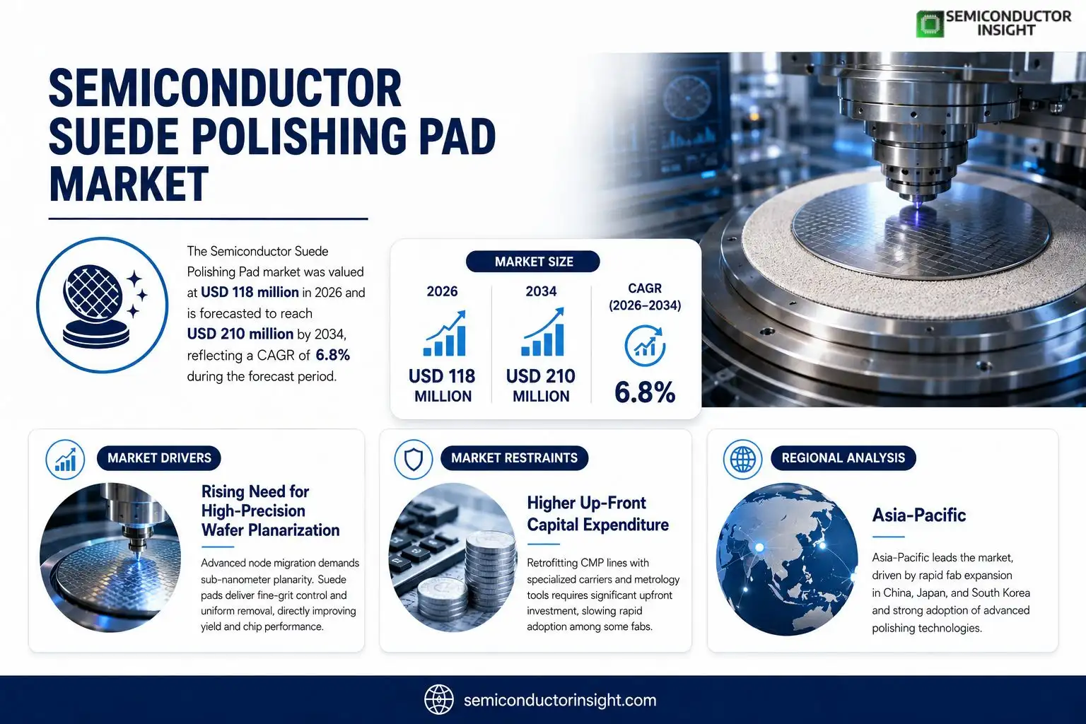
Semiconductor Suede Polishing Pad Market size was valued at USD 118 million in 2026 and is forecasted to reach USD 210 million by 2034, reflecting a compound annual growth rate of approximately 6.8% over the projection horizon.
Semiconductor suede polishing pads are engineered composite media used for fine‑grit planarization of silicon, sapphire and compound wafers during advanced node fabrication. Their porous suede surface combined with a resilient base enables uniform material removal while minimizing defect generation, making them essential for high‑yield semiconductor manufacturing.The Market expansion is underpinned by rising demand for higher‑density chips, increased capital spending on fab upgrades, and ongoing process‑optimization initiatives across leading foundries. Key manufacturers such as Chiyoda, Fujibo Holdings, Spartan Felt Company, Baikowski and FILWEL continue to invest in material innovations and capacity enhancements to meet evolving customer specifications.
Market DRIVERS
Rising Need for High‑Precision Wafer Planarization
Manufacturers of advanced logic and memory chips are increasingly constrained by surface uniformity requirements. Semiconductor Suede Polishing Pad Market solutions provide the fine‑grit control essential for sub‑nanometer planarity, directly influencing yield and performance. The trend stems from the migration toward nodes below 10 nm, where any residual topography translates into electrical variability.
Shift Toward Low‑Defect Polishing Materials
Traditional abrasive carriers generate particulate contamination that can impair device reliability. Suede‑based pads, characterized by their soft, non‑abrasive substrate, reduce defect introduction while maintaining material removal rates. This balance has prompted fabs to replace conventional pads with suede variants, especially in critical polishing steps such as CMP of copper interconnects.
➤ Operators report up to a 15 % reduction in defect density when transitioning to suede polishing pads, accelerating time‑to‑Market for cutting‑edge products.
The cumulative effect of tighter tolerances and lower defectivity is fostering a steady investment cycle in suede‑pad technology, encouraging both original equipment manufacturers and specialty chemical firms to broaden their product portfolios.
Market CHALLENGES
Material Compatibility Issues
While suede pads excel in minimizing scratches, they can exhibit excess compliance on harder dielectric layers, leading to uneven material removal. Engineers must carefully match pad hardness to specific stack compositions, a process that adds cycle‑time and calibration overhead.
Other Challenges
Supply Chain Constraints
The proprietary polymer blends used in suede pad cores are sourced from a limited number of suppliers. Recent geopolitical tensions have intermittently disrupted raw‑material shipments, prompting fabs to maintain higher safety stocks and potentially inflating operational costs.Additionally, the learning curve associated with optimal pad conditioning protocols can slow adoption in facilities that have entrenched legacy processes, limiting the speed at which the Market expands.
Market RESTRAINTS
Higher Up‑Front Capital Expenditure
Implementing suede‑based polishing stations often requires retrofitting existing CMP lines with specialized carriers and metrology tools. The initial outlay can be substantial, especially for mid‑size fabs operating under tight CAPEX budgets. This financial hurdle discourages some players from rapid migration, slowing overall Market momentum.
Market OPPORTUNITIES
Emergence of 3D‑Stacked Architectures
Three‑dimensional integration demands repetitive planarization of tightly packed layers. Suede pads, with their ability to deliver consistent removal across diverse material stacks, are uniquely positioned to support this architectural shift. Companies that can tailor pad formulations to the nuanced demands of TSV (through‑silicon‑via) polishing stand to capture a growing share of the high‑value segment.
Semiconductor Suede Polishing Pad Market Trends
Shift Toward Soft‑Base Materials
The Semiconductor Suede Polishing Pad Market is witnessing a measurable transition from traditional hard‑base formulations toward soft‑base constructions. Customers in advanced wafer processing have reported higher uniformity and reduced defect rates when employing pads with compliant substrates, prompting equipment manufacturers to redesign polishing kits. This movement is reinforced by the growing adoption of 300‑mm silicon wafer platforms, where surface integrity commands premium pricing. As a result, suppliers are reallocating R&D budgets to enhance pad elasticity while maintaining removal efficiency, a balance that directly influences factory throughput. The shift also aligns with tighter specifications from leading fabs that prioritize low‑particle generation. Vendors that can deliver a soft‑base product meeting these criteria are gaining access to higher‑margin contracts, especially in regions where new fabs are being commissioned.
Other Trends
Regional Demand Realignment
In North America, the United States continues to dominate demand, supported by investment in legacy and leading‑edge fabs. Meanwhile, Chinese manufacturers are expanding capacity, reflected in their projected multi‑million‑unit purchases over the next decade. This divergent growth pattern forces players to calibrate supply chains, often establishing localized production hubs to mitigate lead‑time pressures. Europe displays moderate growth, with Germany and the United Kingdom maintaining steady orders, while emerging Asian economies such as South Korea and India are beginning to place initial volumes, indicating a gradual broadening of the Market footprint.
Competitive Consolidation Emerging
Competitive dynamics are sharpening as the top five players command a sizable share of revenue. Recent M&A activity illustrates a strategic push to secure specialty polymer lines and broaden product portfolios. At the same time, environmental regulations are nudging firms to develop pads with recyclable backings, a development that could reshape cost structures and open niche Markets for eco‑focused suppliers. Companies that combine advanced material engineering with sustainable design are likely to capture the most attractive opportunities as customer expectations evolve toward both performance and responsibility.
COMPETITIVE LANDSCAPE
Key Industry Players
Semiconductor Suede Polishing Pad Market: Competitive Overview
Chiyoda Corporation dominates the high‑performance segment of the semiconductor suede polishing pad Market, leveraging its deep expertise in advanced ceramics and long‑standing relationships with leading wafer fabs. The company’s ability to co‑develop custom pad formulations with equipment OEMs has entrenched its position as a preferred supplier for 300‑mm silicon wafer lines. This strategic alignment translates into a sizeable share of revenue and gives Chiyoda leverage in pricing negotiations, as buyers often tie pad procurement to broader wafer‑processing contracts. The Market structure therefore reflects a classic “top‑heavy” configuration where a few large integrators control the bulk of volume, while smaller, specialist firms chase niche applications such as sapphire and compound wafers. The concentration encourages consolidation activity, as mid‑size players seek scale to meet the increasing demand for thinner, defect‑free substrates.Beyond Chiyoda, a cadre of specialized manufacturers sustains competitive pressure. Fujibo Holdings distinguishes itself through a diversified portfolio that pairs suede pads with proprietary backing materials, enabling rapid cycle‑time reductions for thin‑film processes. Spartan Felt Company exploits its historic know‑how in textile engineering to offer pads with superior wear‑uniformity, a trait prized by fabs targeting sub‑10 nm nodes. Baikowski and FILWEL focus on medium‑hard and PET‑based pads, respectively, serving customers that prioritize surface‑finish consistency over outright throughput. Regional players such as Nitto Denko (Japan), Tokuyama Corporation (Japan), and Advanced Materials Ltd. (UK) provide localized support and faster logistics, which become decisive factors for fabs operating in Asia‑Pacific. Collectively, these niche firms inject innovation into the supply chain, compelling the incumbents to continuously upgrade their product lines and maintain service excellence.
List of Key Semiconductor Suede Polishing Pad Companies Profiled
- Chiyoda Corporation
- Fujibo Holdings
- Spartan Felt Company
- Baikowski
- FILWEL
- Nitto Denko
- Tokuyama Corporation
- Advanced Materials Ltd.
- 3M Precision Polishing
- Sumitomo Chemical Co.
- Kureha Corporation
- Sunon International
Segment Analysis:
| Segment Category | Sub-Segments | Key Insights |
| By Type |
|
Soft Base dominates due to its superior conformity and low‑damage characteristics.
|
| By Application |
|
Silicon Wafer remains the primary application driver.
|
| By End User |
|
Semiconductor Fabricators lead adoption because of the direct impact on product yield.
|
| By Process Stage |
|
Fine Polishing is gaining traction as device geometries shrink.
|
| By Material Compatibility |
|
Oxide Wafer remains the cornerstone of compatibility considerations.
|
Regional Analysis: Semiconductor Suede Polishing Pad Market
North America
Declining transistor dimensions and the rise of heterogeneous integration push fab operators to seek pads that deliver uniform material removal while preserving surface integrity, directly boosting demand for specialised suede formulations.
A concentrated network of both legacy and emerging pad manufacturers serves North America, with many firms establishing local R&D hubs to accelerate prototyping cycles and reduce lead times.
Stringent environmental regulations around abrasive waste encourage suppliers to develop recyclable pad substrates, aligning compliance needs with cost‑efficiency goals for end users.
Market participants differentiate through bespoke pad textures and hybrid bonding agents, creating niche advantages that are often protected by patents and exclusive supply agreements.
Europe
European fabs are increasingly orientated toward sustainability, prompting a gradual transition to suede pads that incorporate bio‑based binders. This environmental focus dovetails with the region’s strong engineering talent pool, which fuels collaborative projects between pad makers and research institutes. Consequently, Europe is witnessing a subtle re‑allocation of R&D spend toward low‑defect polishing chemistries that support advanced packaging formats such as fan‑out wafer‑level packaging. The ripple effect is a modest but steady expansion of niche supplier networks that cater to high‑mix, low‑volume production lines typical of the region’s specialty semiconductor sector.
Asia‑Pacific
Asia‑Pacific’s rapid capacity expansion, driven by both established foundries and new entrants, creates a fertile ground for adoption of high‑performance suede pads. Operators are confronted with the dual challenge of scaling output while maintaining tight defect budgets, a scenario that elevates the importance of pad consistency across large wafer volumes. Local manufacturers are responding by scaling up pilot lines that trial innovative abrasive blends, often in partnership with equipment OEMs. The region’s cost‑sensitive environment also encourages the development of hybrid pads that balance performance with price, ensuring that emerging players can access technology without prohibitive upfront expenditure.
South America
South American semiconductor activity remains concentrated around assembly, testing, and modest fabrication capabilities, yet the Market is beginning to feel the influence of fab upgrades. Companies are importing suede pads to support retro‑fit polishing stations, aiming to improve throughput on legacy process nodes. As regional investment in advanced manufacturing zones gathers pace, the demand for pads that can adapt to a range of wafer sizes and materials is expected to rise, prompting a gradual diversification of the local supplier base.
Middle East & Africa
The Middle East & Africa region, while still nascent in semiconductor production, is leveraging its strategic logistics hubs to become a redistribution corridor for premium polishing pads. Emerging technology parks are attracting multinational fab operators seeking cost‑effective expansion outside traditional hubs. In response, pad vendors are establishing regional service centers to provide rapid technical support and spare‑part logistics, a move that mitigates downtime risks for customers operating in less‑developed industrial ecosystems.
Report Scope
This Market research report provides a comprehensive analysis of the Semiconductor Suede Polishing Pad Market , covering the forecast period 2026–2034. It offers detailed insights into Market dynamics, technological advancements, competitive landscape, and key trends shaping the industry.
Key focus areas of the report include:
- Market Overview: The report begins with an overview outlining its current Market scenario, key growth indicators, and industry transformation drivers. It discusses macroeconomic factors, demand–supply balance, regulatory landscape, and the strategic role of semiconductors in powering advancements across industries such as automotive, telecommunications, consumer electronics, and industrial automation.
- Market Size & Forecast: Historical data and future projections for revenue, unit shipments, and Market value across major regions and segments.
- Segmentation Analysis: Detailed breakdown by product type, technology, application, and end-user industry to identify high-growth segments and investment opportunities.
- Regional Insights: Insights into Market performance across North America, Europe, Asia-Pacific, Latin America, and the Middle East & Africa, including country-level analysis where relevant.
- Competitive Landscape: Profiles of leading Market participants, including their product offerings, R&D focus, manufacturing capacity, pricing strategies, and recent developments such as mergers, acquisitions, and partnerships.
- Technology Trends & Innovation: Assessment of emerging technologies, integration of AI/IoT, semiconductor design trends, fabrication techniques, and evolving industry standards.
- Market Drivers & Restraints: Evaluation of factors driving Market growth along with challenges, supply chain constraints, regulatory issues, and Market-entry barriers.
- Stakeholder Insights: Insights for component suppliers, OEMs, system integrators, investors, and policymakers regarding the evolving ecosystem and strategic opportunities.
Primary and secondary research methods are employed, including interviews with industry experts, data from verified sources, and real-time Market intelligence to ensure the accuracy and reliability of the insights presented.
FREQUENTLY ASKED QUESTIONS:
What is the current Market size of Semiconductor Suede Polishing Pad Market?
-> Semiconductor Suede Polishing Pad Market was valued at USD million in 2026 and is projected to reach USD million by 2034, at a CAGR of % during the forecast period.
Which key companies operate in Semiconductor Suede Polishing Pad Market?
-> Key players include Chiyoda, Fujibo Holdings, Spartan Felt Company, Baikowski, FILWEL, among others.
What are the key growth drivers?
-> Key growth drivers include rising demand for high‑precision wafer polishing, expansion of semiconductor manufacturing capacity, and adoption of advanced materials such as silicon, sapphire and compound wafers.
Which region dominates the Market?
-> Asia dominates the Market, with China projected as the largest contributor while the U.S. Market is estimated at USD million in 2025.
What are the emerging trends?
-> Emerging trends include growth of the Soft Base segment, development of PET Base and medium‑hard base technologies, and increasing focus on sustainable polishing solutions.
Get Sample Report PDF for Exclusive Insights
Report Sample Includes
- Table of Contents
- List of Tables & Figures
- Charts, Research Methodology, and more...
 Download Sample Report PDF