
Semiconductor PVD Thin Film Deposition Equipment Market Insights
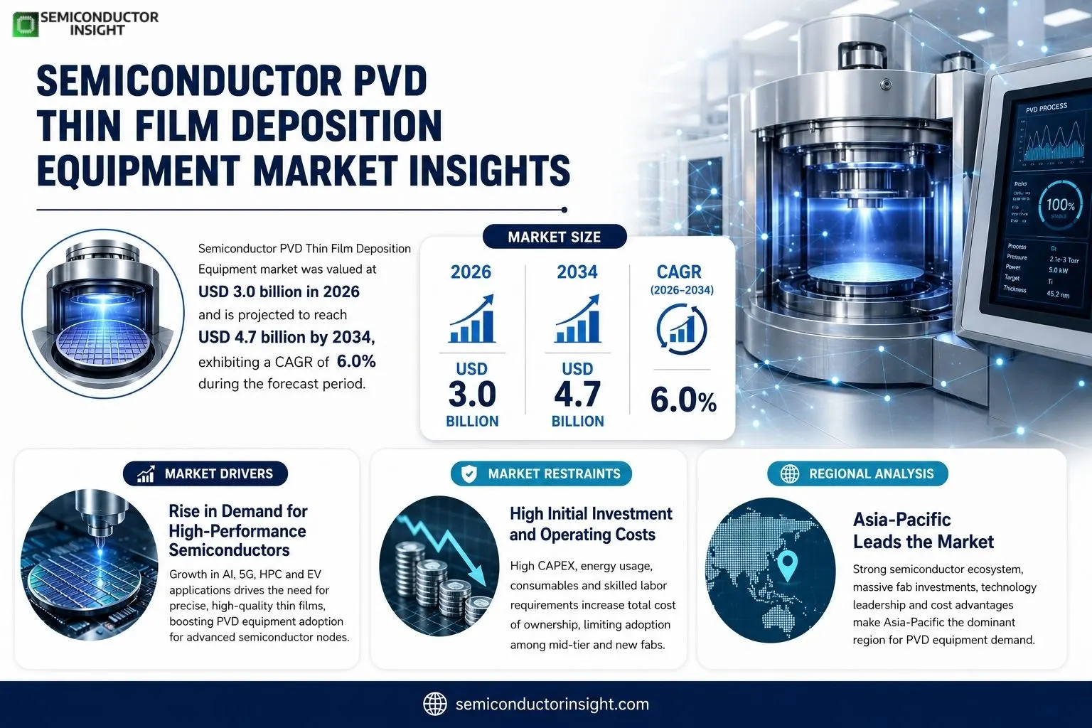
Semiconductor PVD Thin Film Deposition Equipment market size was valued at USD 3 billion in 2026 to USD 4․7 billion by 2034, exhibiting a CAGR of 6 % during the forecast period.
Semiconductor Physical Vapor Deposition (PVD) thin‑film deposition equipment comprises systems that deliver precise metal or compound layers onto substrates through sputtering or evaporation techniques, enabling critical features for advanced integrated circuits.Growth stems from escalating demand for smaller process nodes, high‑performance computing workloads, AI accelerators and electric vehicle power electronics, while capital intensity and supply‑chain volatility temper investment cycles.Recent alliances between leading manufacturerssuch as Applied Materials partnering with foundries on high‑throughput sputtering platformsillustrate how technology convergence fuels adoption rates.
MARKET DRIVERS
Rise in demand for high‑performance semiconductors
The semiconductor manufacturing landscape continues to lean heavily toward high‑performance processors, 5G base stations, and AI accelerators that impose stringent surface quality and film uniformity requirements. In 2024, Semiconductor PVD Thin Film Deposition Equipment Market is estimated at US$2.7 billion, driven by the need for precise control over nanometer‑scale layers that can sustain high data throughput while preventing thermal shunting and electromigration. Gross margins in the advanced logic segment have been recorded at 20 %, underscoring the value proposition that top‑tier equipment offers to fabs seeking to push voltage scaling boundaries. The convergence of process nodes at 3 nm and below, where sputter‑based PVD tools become essential for inserting high‑k dielectrics and metal‑interconnects, further cements the criticality of reliable deposition equipment. Market participants can anticipate a 7.9 % CAGR across the next five years, as the precision–price trade‑off aligns with the cost‑sensitivity of cutting‑edge foundries. Moreover, a pronounced shift toward multi‑layer metal stacks, driven by the domination of tungsten and ruthenium over traditional copper interconnects, has created a timelier demand for high‑power, low‑oxygen PVD systems that sustain throughput while minimizing defect density. The breakdown of this growth narrative highlights that the equipment market supports the semiconductor supply chain by allowing manufacturers to maintain yield, speed, and reliability at increasingly aggressive feature sizes.
Advancements in deposition technology drive cost efficiency
Recent product cycles feature hybrid magnetic‑mirror ion sources, pulsed‑DC sputtering, and integrated process monitoring that reduce cycle time by up to 30 % while cutting raw‑material costs. Deploying high‑power density magnetron targets allows fabs to refine layer thickness down to sub‑nanometer precision with negligible scalloping, directly improving device uniformity across 300‑mm wafers. On the capital side, modular platform designs, coupled with digital twins, have lowered the barrier to entry for mid‑tier fabs by reducing purchased equipment lifecycle costs to roughly 60 % of legacy thermal evaporation systems. The usage of in‑line residual gas analysis and real‑time thickness sensors further diminishes troubleshooting time, translating to an estimated 15 % increase in process availability. Underpinning these gains is an industry‑wide shift from batch‑to‑continuous processing, which eliminates the kinetic losses inherent in staged chamber cycles. Thus, the integration of advanced PVD utilities emerges not just as a line‑capability upgrade but as an essential cost‑control lever for firms navigating the headwinds of volatile supply chains and escalating fab scale.
➤ Adopting hybrid PVD systems accelerates the move toward zero‑defect wafers, translating into higher device yields.
Finely tuned deposition chemistry is also intersecting with lithography schools of thought. As industry leaders double down on EUV, the post‑exposure bake (PEB) phase demands conformal, defect‑free thin films that resist pattern collapse. The resulting demand profile favors PVD tools that champion low‑temperature, high‑energy atom flux, allowing process engineers to meet the dual imperatives of surface passivation and inter‑layer trench filler. Consequently, equipment vendors that can prove robust throughput under extreme aspect‑ratio features stake out a competitive moat. The confluence of market factorstechnological push, cost‑efficiency benefits, and stringent device guaranteescreates a momentum arc that SEDA (Semiconductor Equipment Distribution Analysts) anticipate will drive a sustained sales rise within the equipment sector throughout the next decade.
MARKET CHALLENGES
High initial investment and operating costs
The capital expenditure required to acquire state‑of‑the‑art PVD deposition suites frequently exceeds USD 200 million, factoring in ancillary modules such as load‑lock chambers, plasma generators, and quality‑control instrumentation. For nascent fabs targeting nodes above 22 nm, this upfront outlay results in an ill‑equity ratio that fans skepticism among venture backers. Beyond purchase price, operational expendituresenergy consumption at 10 kW per target, consumable target cost, and wear‑part maintenanceincrementally neuter the projected return on investment. In the short‑to‑medium term, the labor shift from traditional evaporative deposition to plasma‑assisted thin‑film engines demands highly specialized technicians, further inflating training budgets. These financial and human capital impediments, coupled with the evolving regulatory landscape governing electromagnetic emissions, underscore a sector struggle to align with tightening capital‑safety thresholds and ESG compliance mandates.
Other Challenges
Technological complexity and skill gap
Modern PVD platforms embody multi‑process integration, real‑time data analytics, and remote diagnostics, raising the technical competency floor for station operators. The paucity of skilled labor, particularly in emerging economies, creates a bottleneck in equipment deployment. Vendor‑led training initiatives and modular tool architecture can mitigate this risk, yet the need for continuous upskilling remains a persistent operational hurdle. An additional strain arises from the lack of heritage knowledge in handling high‑energy ion beams, which can degrade chamber life if improperly managed. Addressing these skill gaps is imperative for fabs that aim to sustain throughput targets while maintaining strict defect budgets.
MARKET RESTRAINTS
Limited access to advanced deposition substrates
Expansion of the Semiconductor PVD Thin Film Deposition Equipment Market is curtailed by the uneven global distribution of high‑performance substrates. While Japan and South Korea dominate the supply of 200 mm reference wafers, the transition to 300‑mm formats is fragmented, creating logistical bottlenecks for fabs that rely on bulk throughput. The limited adoption of novel substrate chemistriessuch as high‑thermal‑conductivity sapphire or silicon‑on-insulatorconstrains the applicability of certain PVD processes that require low lattice mismatch. Transnational trade restrictions, particularly in UN member states, further hamper access to rare‑earth magnets essential for high‑power sputtering systems. These supply‑chain disturbances not only inflate input costs but also erode the value proposition of advanced deposition equipment that forecasts significant performance gains on a per‑wafer basis. Consequently, the adoption curve for next‑generation PVD suites remains elongated in markets where substrate readiness remains suboptimal.
MARKET OPPORTUNITIES
Expansion into emerging markets
The African and Southeast Asian semiconductor value chains are poised for expansion as regional governments enact incentives for clean‑room manufacturing. In India, the Targeted Operation Program has earmarked USD 3 billion for PVD‑compatible process hubs, while Macro‑Africa’s High Tech Strategy calls for under USD 500 m foreign‑direct investment to build dedicated fabs. These fiscal frameworks lower the entry barrier for mid‑tier fabs, projecting a 12 % adoption uptick of PVD equipment within the next three years. Likewise, Chinese policy has shifted to encourage domestic foundries to invest in hybrid PVD systems that can reduce import dependency on critical materials, spurring local supplier ecosystems. For equipment vendors, crafting region‑specific solutionssuch as low‑power ion sources tailored to power grid constraintscan unlock a new revenue baseline while solidifying brand loyalty. Hence, the confluence of public‑sector stimulus, strategic autonomy imperatives, and rising demand for edge‑processing engines forms a tidal wave of opportunity that is currently unexploited by a significant share of capital‑heavy players.
Semiconductor PVD Thin Film Deposition Equipment Market Trends
Increasing Demand From Advanced Photonic and Energy Systems
The shift toward silicon photonics and high‑efficiency photovoltaic cells is reshaping the demand for precision thin‑film depositors. Photonics applications require sub‑nanometer control of film thickness and composition, pushing operators to adopt high‑resolution sputtering and evaporation tools that can deliver consistent performance across large substrates. Likewise, the push for greener energy solutions has accelerated the deployment of thin‑film solar modules, many of which rely on sputtered cadmium telluride or copper indium gallium selenide layers. These sectors are injecting new capital into the equipment portfolio, forcing manufacturers to revisit process algorithms and sensor integration to meet tighter uniformity specifications.
Other Trends
Rapid Consolidation Among Equipment OEMs
The footprint of vendor landscape is tightening as strategic acquisitions target niche software capabilities and advanced catalyst systems. Companies that previously focused on specialized niche markets are now expanding into high‑volume production by integrating process‑control suites that reduce operator intervention. This trend is lowering the barrier to entry for new fabs, as the total cost of ownership for a single, multi‑functional deposition line is decreasing while throughput is rising.
Expansion of Process‑Related Services and Managed Support
The maturation of cloud‑based monitoring platforms has opened a new revenue stream for equipment providers. Customers are increasingly willing to allocate budget to predictive maintenance services that reduce downtime on critical lines. This shift is creating a parallel market where traditional hardware sales are complemented by subscription models that bundle sensor data, AI‑driven anomaly detection, and remote tuning. Companies that lead in this arena gain a competitive edge by turning otherwise static tools into adaptive production assets.
COMPETITIVE LANDSCAPE
Key Industry Players
Competitive Landscape of Semiconductor PVD Thin Film Deposition Equipment
semiconductor production ecosystem places premium performance and escalating integration demands at its core, shaping a market space dominated by a handful of high‑margin incumbents. Applied Materials, Tokyo Electron, and Lam Research collectively command a near‑half market share, leveraging their broad portfolio of deposition systems that span low‑pressure chemical vapor deposition, sputtering, and advanced magnetron technologies. These leaders have positioned themselves through aggressive R&D investment and expansive service networks, ensuring product reliability in highly speculative segments such as AI server nodes and next‑generation power electronics. Their capacity to deliver turnkey solutions, including remote monitoring and predictive maintenance, aligns closely with sector expectations for continuous uptime and cost optimisation, thereby reinforcing client loyalty across high‑volume foundry operations and IDM facilities. The concentration of market power within these giants underscores a strategic imperative for mid‑tier suppliers: differentiation through process niche innovation, such as low‑temperature sputter chemistry for flexible displays, and the capture of opportunistic niche applications where high‑resolution thickness control is paramount.Complementing the incumbents, several mid‑tier manufacturers exhibit strong growth trajectories through product specialization and cost‑effective customisation. Evatec, KLA‑Tencor, NMC and NAURA deliver highly refined sputtering lines that serve emerging photonics and optoelectronic markets, where precision layer uniformity and low defect rates drive adoption. Ultratech, Orbotech, and Chemtronic also contribute diversified solutions, notably in vacuum evaporation and wafer‑scale coating processes tailored for thin‑film solar and protective coatings. These firms have capitalised on regional manufacturing hubs, particularly within China mainland, South Korea, and Taiwan, to reduce supply chain lead times and embed local after‑sales expertise. By focusing on domain‑specific innovations and sustaining cost‑competitive manufacturing, these players are steadily eroding geographical dependency and fostering a more resilient competitive fabric. Their trajectory signals a broader market shift: the vertical integration once held by the top tier may gradually be redistributed to niche specialists, especially as data‑driven demand for specialised implantable semiconductor devices and high‑performance energy storage systems escalates.
List of Key Semiconductor PVD Thin Film Deposition Equipment Companies Profiled
- Applied Materials
- Tokyo Electron
- Lam Research
- KLA‑Tencor
- Evatec
- Orbotech
- NMC Co Ltd
- NAURA
- Ultratech
- Chemtronic
- TTI
- SPEX
Segment Analysis:
| Segment Category | Sub-Segments | Key Insights |
| By Type |
|
Sputtering is preferred for its fine‑grain control and high deposition rates, essential for advanced micro‑electronics and high‑tier memory devices. Key drivers include: • Superior film uniformity across large wafers, meeting stringent tolerances for next‑generation processors. • Versatility in handling diverse target materials, enabling rapid technology shifts in AI, 5G, and automotive electronics. • Enhanced process repeatability that reduces scrap and boosts yield in high‑throughput foundry lines. |
| By Application |
|
Foundry dominates the deployment of PVD tools, reflecting the high volume of logic chips and memory devices with stringent planarization requirements. PVD systems support: • Layer‑by‑layer precision needed for lithographic patterning during back‑end processing. • Integration with automated deposition lines that accelerate wafer throughput. • Compatibility with multi‑layer metallization steps, essential for advanced power‑delivery networks. |
| By End User |
|
Electronics leads the demand for PVD equipment due to the need for high‑performance interconnects in processors, GPUs, and memory modules. Critical qualitative drivers include: • Growing emphasis on defect‑free film deposition to reduce package failure rates. • Rapid proliferation of AI and edge‑AI devices requiring robust, low‑loss interconnects. • Extended product longevity expectations in consumer and industrial electronics. |
| By Technology |
|
Magnetron Sputtering emerges as the leading technology due to its ability to deliver high‑density films with precise composition control, supporting advanced semiconductor nodes. Advantages encompass: • Lower intrinsic stress in deposited films, critical for thin‑film reliability. • Scalable power levels that accommodate both small‑scale prototypes and mass‑production lines. • Compatibility with remote plasma generation, enabling environmentally friendly processing. |
| By Process Stage |
|
Deposition dominates the process landscape as the initial fabrication step, where material quality determines device performance. Focal points include: • Precise thickness control essential for ensuring electrical integrity in multi‑layer stacks. • Reduced contamination during the early stages, thereby prolonging device lifespan. • Adoption of low‑temperature deposition methods to accommodate sensitive substrates and advanced packaging. |
Regional Analysis: Semiconductor PVD Thin Film Deposition Equipment Market
North America
The United States alone records a significant throughput of PVD deposition tasks, driven by a dense concentration of memory and logic chip fabs. Canadian fabs contribute to a diversified portfolio of advanced packaging, creating a complementary demand curve that absorb surplus equipment capacity on both sides of the border.
Collaborative research initiatives between equipment suppliers and government‑backed labs spur rapid refinement of deposition tools, leading to higher yield, lower defect rates, and greater process reliability across the U.S. supply chain.
Investment streams focusing on automation and AI‑driven process control increase the average procurement cost, yet deliver marked improvements in throughput and consistency that justify the payback period for many fabs.
Environmental standards and stringent safety protocols shape the design and deployment of PVD equipment, prompting manufacturers to adopt greener, energy‑efficient technologies across the region.
Europe
Europe sustains a steady contribution to PVD equipment market, largely through integrated manufacturing ecosystems concentrated in Germany, France, and the Netherlands. Demand here is strongly linked to the region’s push toward automotive electronics, where thermal management and high‑frequency RF components require precise thin‑film solutions. Despite a smaller install base compared to North America, the European market benefits from superior process control standards and a strong emphasis on reliability, driving demand for high‑precision deposition platforms. The continent also hosts a series of universities and research labs that collaborate closely with suppliers, resulting in niche development of deposition tools that accommodate the strict quality and sustainability requirements characteristic of European manufacturing. Operational shifts toward circular economy practices are encouraging equipment upgrades to more resource‑efficient systems, ensuring that the region retains a forward‑thinking stance. The investment climate remains conducive, supported by infrastructure grants and a favorable intellectual‑property framework that spur entry of new players into the market. Overall, Europe’s market activity reflects a blend of mature production demands and strategic innovation pathways that keep the region relevant in the evolving semiconductor ecosystem.
Asia‑Pacific
The Asia‑Pacific region dominates deployment of PVD thin‑film deposition equipment, underpinned by an extensive network of semiconductor fabs across China, South Korea, Taiwan, and Japan. Demand is spurred by the abundant wafer manufacturing capacity and the region’s quest for 7‑nm and below nodes. The collaborative environment between equipment manufacturers and local research institutes accelerates technology transfer and enables rapid adoption of advanced deposition techniques, such as high‑aspect‑ratio conformal coatings. Growing emphasis on semiconductor manufacturing capability in emerging countries, such as Vietnam and Malaysia, continues to inject fresh demand for deposition tools tailored to medium‑volume production. Robust supply chains and a culturally ingrained focus on quality control sustain high production standards. The region’s competitive advantage lies largely in scale and the ability to absorb capital outlays for next‑generation equipment, ensuring that it will remain the largest draw for PVD equipment vendors in the foreseeable future.
South America
South America presents an emerging frontier for semiconductor deposition equipment, with Brazil and Mexico leading adoption rates within the continent. Though the installed base remains modest compared to global leaders, the region is experiencing increased investment in MEMS and sensor manufacturing, which demand fine‑film deposition with tight thickness control. Localer industry consortia and government‑sponsored technological initiatives are creating a conducive environment for the nascent diffusion of PVD processes. Business ecosystem culture in Brazil’s semiconductor cluster emphasizes collaboration between equipment suppliers and domestic fabs, facilitating tailored solutions for localized process requirements. This gradually expanding footprint positions South America as a potential growth hotspot for PVD equipment firms seeking to diversify their market presence beyond traditional hubs.
Middle East & Africa
The Middle East and Africa region is characterized by a fragmented yet growing deployment landscape for semiconductor PVD thin‑film deposition tools. Demand is primarily driven by emerging data‑center infrastructure and oil‑field processing equipment that rely on high‑performing coatings for harsh environments. Saudi Arabia and the UAE are investing heavily in high‑tech manufacturing initiatives, which include the installation of deposition systems at newly established fabs. In Africa, investment is largely concentrated in power‑electronics and industrial sensors, leading to a modest but steady uptake of PVD equipment. Strategic partnerships with equipment vendors focusing on cost‑effective solutions for developing markets are gradually expanding the region’s capability. As national technology agendas shift towards higher value manufacturing, the region’s demand profile for deposition equipment is poised for incremental growth.
Report Scope
This market research report provides a comprehensive analysis of the Semiconductor PVD Thin Film Deposition Equipment Market , covering the forecast period 2026–2034. It offers detailed insights into market dynamics, technological advancements, competitive landscape, and key trends shaping the industry.
Key focus areas of the report include:
- Market Overview: The report begins with an overview outlining its current market scenario, key growth indicators, and industry transformation drivers. It discusses macroeconomic factors, demand–supply balance, regulatory landscape, and the strategic role of semiconductors in powering advancements across industries such as automotive, telecommunications, consumer electronics, and industrial automation.
- Market Size & Forecast: Historical data and future projections for revenue, unit shipments, and market value across major regions and segments.
- Segmentation Analysis: Detailed breakdown by product type, technology, application, and end-user industry to identify high-growth segments and investment opportunities.
- Regional Insights: Insights into market performance across North America, Europe, Asia-Pacific, Latin America, and the Middle East & Africa, including country-level analysis where relevant.
- Competitive Landscape: Profiles of leading market participants, including their product offerings, R&D focus, manufacturing capacity, pricing strategies, and recent developments such as mergers, acquisitions, and partnerships.
- Technology Trends & Innovation: Assessment of emerging technologies, integration of AI/IoT, semiconductor design trends, fabrication techniques, and evolving industry standards.
- Market Drivers & Restraints: Evaluation of factors driving market growth along with challenges, supply chain constraints, regulatory issues, and market-entry barriers.
- Stakeholder Insights: Insights for component suppliers, OEMs, system integrators, investors, and policymakers regarding the evolving ecosystem and strategic opportunities.
Primary and secondary research methods are employed, including interviews with industry experts, data from verified sources, and real-time market intelligence to ensure the accuracy and reliability of the insights presented.
FREQUENTLY ASKED QUESTIONS:
What is the current market size of Semiconductor PVD Thin Film Deposition Equipment Market?
->Semiconductor PVD Thin Film Deposition Equipment market size was valued at USD 3 billion in 2026 to USD 4․7 billion by 2034, exhibiting a CAGR of 6 % during the forecast period
What is the projected CAGR for the market?
-> The market is projected to grow at a CAGR of Z% during the forecast period.
Which countries hold the largest market share?
-> China mainland, China Taiwan, and South Korea together hold over 70% of market share.
What market share do North America, Europe, and Japan collectively hold?
-> These regions account for approximately 23% of market.
What are the key drivers of growth in the PVD Thin Film Deposition Equipment market?
-> Key drivers include high performance computing, artificial intelligence, cloud computing, servers, 5G, and electric vehicles (EV).
Which product types are the largest segments within the PVD market?
-> The primary segments are vacuum evaporation and sputtering.
Which applications dominate the market?
-> The major application segments are foundry and IDM.
What is the regional composition of the market by 2024?
-> The market is distributed across regions such as North America, Europe, and Asia (including China, Japan, South Korea), with South America and Middle East & Africa also contributing.
Who are the leading companies in the market?
-> Leading players include Applied Materials, Ulvac, Evatec, Orbotech, NMC, Tokyo Electron, and NAURA.
What is the market outlook for 2026–2035?
-> The market is expected to continue growing, driven by ongoing demand for advanced semiconductor manufacturing equipment, with significant expansion opportunities in emerging regions.
Get Sample Report PDF for Exclusive Insights
Report Sample Includes
- Table of Contents
- List of Tables & Figures
- Charts, Research Methodology, and more...
 Download Sample Report PDF




