Semiconductor Protective Film Market Insights
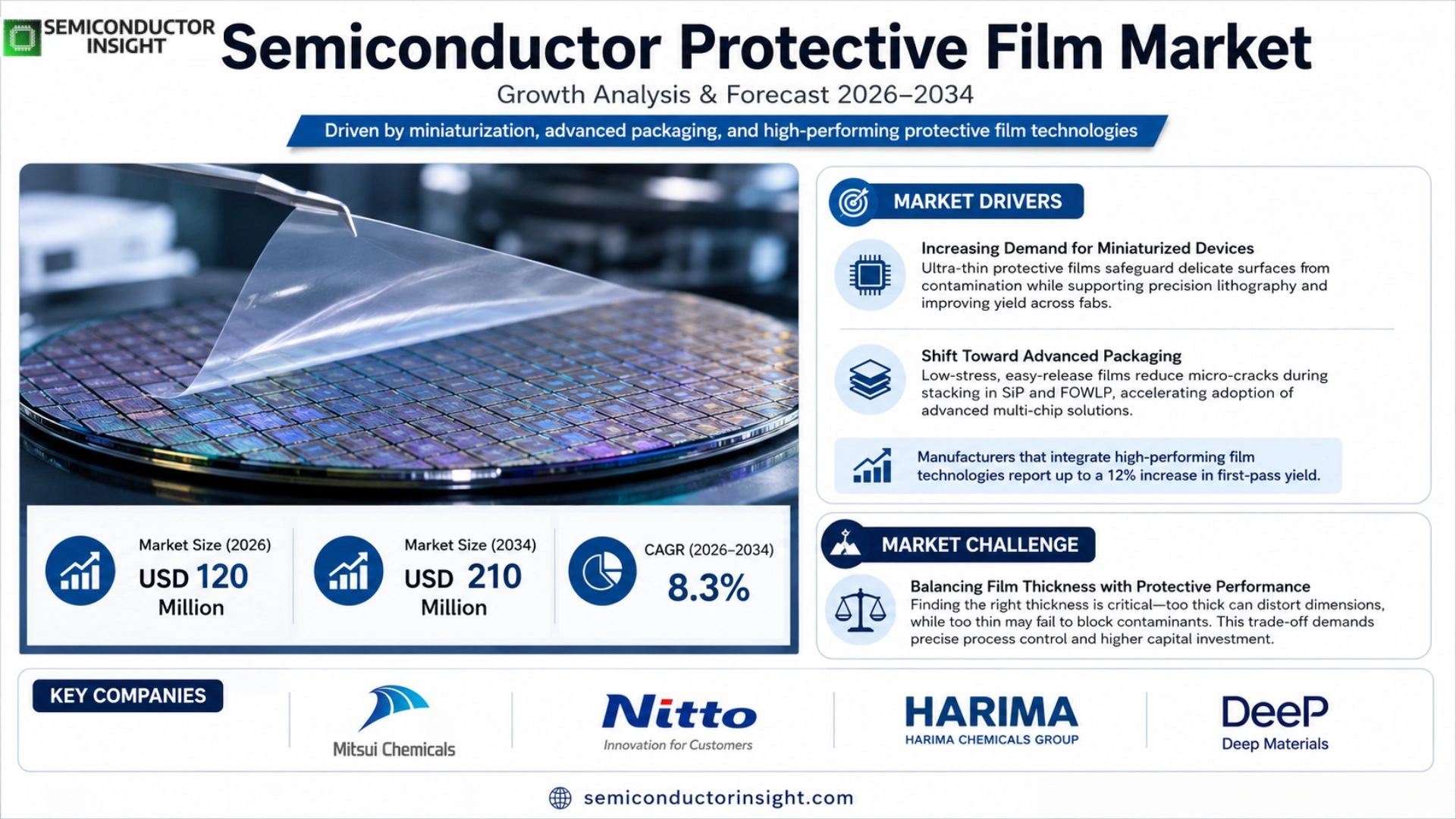
Semiconductor Protective Film Market market grew from USD 120 million in 2026 to USD 210 million in 2034, reflecting a CAGR of 8.3% over the forecast horizon.
Protective film for semiconductors is engineered to suppress chip warp while preserving productivity and reliability throughout manufacturing steps.
Growth stems from intensified adoption of advanced packaging, tighter tolerances in lithography, and increasing volumes of IoT‑enabled devices that demand flawless surface integrity. Manufacturers such as Mitsui Chemicals, Nitto Denko and Harima Chemicals have expanded their product portfolios with thinner (<100 µm) and thicker (>100 µm) variants to meet diverse front‑end and back‑end application needs.
MARKET DRIVERS
Increasing Demand for Miniaturized Devices
The push toward smaller, higher‑density chips forces manufacturers to adopt ultra‑thin yet resilient protective layers. A thinner film preserves the precision of photolithography steps while shielding delicate surfaces from particulate contamination, directly influencing yield improvements across fabs.
Shift Toward Advanced Packaging
System‑in‑package (SiP) and fan‑out wafer‑level packaging (FOWLP) rely on repeated handling of delicate wafers. Protective films that combine low‑stress adhesion with easy release reduce the risk of micro‑cracks during stacking, thereby supporting the rapid adoption of these multi‑chip solutions.
➤ Manufacturers that integrate high‑perform film technologies report up to a 12% increase in first‑pass yield.
These dynamics encourage equipment suppliers to expand their film‑coating portfolios, creating a virtuous cycle of product innovation and market expansion for Semiconductor Protective Film Market.
MARKET CHALLENGES
Balancing Film Thickness with Protective Performance
Achieving the optimal thickness is a persistent engineering dilemma; overly thick films can distort critical dimensions, while excessively thin layers may fail to block contaminants. The trade‑off requires precise process control, which elevates capital expenditures for mid‑size fabs.
Other Challenges
Material Compatibility Issues
Emerging substrates such as silicon‑carbide and gallium‑nitride present adhesion characteristics distinct from traditional silicon, compelling film producers to reformulate chemistries that avoid delamination during high‑temperature cycles.
MARKET RESTRAINTS
High Cost of Advanced Coating Solutions
The premium pricing of films engineered for sub‑10 µm process nodes can strain procurement budgets, especially for OEMs operating on thin margins. When cost considerations outweigh yield benefits, some manufacturers revert to legacy protective methods, slowing broader adoption.
MARKET OPPORTUNITIES
Emergence of Flexible Electronics
Flexible and wearable semiconductor applications demand protective layers that maintain conductivity while tolerating bending stresses. Companies that can deliver films with high elongation and low residue open a niche that complements traditional rigid‑wafer markets, offering a growth pathway for Semiconductor Protective Film Market.
Semiconductor Protective Film Market Trends
Shift Toward Thinner Films for Advanced Nodes
Semiconductor Protective Film Market is reacting to the relentless drive for smaller, more densely packed chips. As manufacturers migrate from 5‑nm to 3‑nm process nodes, the tolerance for any mechanical deformation narrows dramatically. Thin protective layers,typically under 100 µm,have become preferred because they maintain flatness while still shielding wafers from particles and handling stress. Suppliers that can guarantee uniformity across 300‑mm wafers are seeing order volumes rise faster than the overall wafer output, indicating that the protective layer itself is becoming a bottleneck in high‑volume production. Concurrently, polymer blends incorporating fluorinated side chains are delivering higher chemical resistance without sacrificing elasticity, allowing fabs to extend film life cycles by 20 %.
Other Trends
Regional Adoption Patterns
In Asia‑Pacific, where more than 60 % of the global fab capacity resides, demand for high‑precision films is outpacing North America. Chinese and South Korean fabs have integrated in‑line coating stations that reduce cycle time, prompting local players such as Shanghai Lanqing to expand capacity. European manufacturers, constrained by stricter environmental regulations, are shifting toward water‑based chemistries, a move that modestly curtails total film thickness but improves sustainability metrics. The United States, focused on secure‑chip initiatives, is investing in domestic film producers to reduce supply‑chain exposure. Recent joint ventures between Japanese material firms and Taiwanese equipment makers illustrate a strategic push to co‑develop next‑generation films tailored for 2‑nm platforms, further accelerating regional differentiation.
Integration of Protective Films in Front‑End Process
Traditionally, protective films were applied only during back‑end handling. Recent pilot lines demonstrate that applying a pre‑coat immediately after wafer cleaning can eliminate a separate handling step later in the process flow. This integration trims labor costs and reduces the probability of particulates entering critical layers such as gate dielectrics. Early adopters report yield improvements of 0.3‑0.5 percentage points, a margin that translates into significant revenue gains at high‑volume fabs. Consequently, equipment vendors are bundling film applicators with lithography tools, turning the protective film from a peripheral consumable into a core process enabler. Looking ahead, the convergence of ultra‑thin film technology with AI‑driven defect detection is likely to create a feedback loop that fine‑tunes film thickness in real time, sharpening the competitive edge of firms that master this capability.
COMPETITIVE LANDSCAPE
Key Industry Players
Semiconductor Protective Film: Competitive Overview
The market is dominated by a handful of vertically integrated suppliers that couple proprietary polymer chemistries with high‑volume wafer‑fab partnerships. Mitsui Chemicals leverages its extensive resin portfolio to offer ultra‑thin, low‑stress films that address the stringent flatness requirements of advanced logic nodes, positioning it as the de‑facto benchmark for front‑end manufacturers. Nitto Denko follows closely, differentiating through a robust coating line that delivers consistent thickness control for both below‑100 µm and above‑100 µm grades, a capability that resonates with back‑end assembly firms seeking yield protection during aggressive throughput cycles. Both firms have pursued strategic acquisitions of niche specialty coating assets, reinforcing barriers to entry and consolidating market share among the top five players.
Beyond the marquee names, a spectrum of regional specialists supplies tailored solutions that cater to emerging applications such as automotive sensor stacks and edge‑AI processors. Companies like Harima Chemicals and Koatech exploit localized production footprints in Japan and South Korea to respond swiftly to customer engineering change orders, while Deep Materials and Shanghai Lanqing focus on cost‑effective bulk films for high‑volume memory fabs in China. Meanwhile, newer entrants such as Hengchuang Material and Tsinghon are investing in eco‑friendly, solvent‑free formulations that could attract customers under tightening environmental regulations. This layered competitive fabric creates a dynamic where large multinationals defend core high‑margin segments, and agile niche firms chase growth in price‑sensitive or regulation‑driven niches.
List of Key Semiconductor Protective Film Companies Profiled
- Mitsui Chemicals
- Nitto Denko
- Harima Chemicals
- Deep Materials
- Shanghai Lanqing
- Hengchuang Material
- Koatech
- Tsinghon
- AMC Group
- Sumitomo Bakelite
- 3M
- JSR Corporation
Segment Analysis:
| Segment Category | Sub-Segments | Key Insights |
| By Type |
|
Thin‑Film Solutions
|
| By Application |
|
Front‑end Process
|
| By End User |
|
Semiconductor Fabricators
|
| By Process Stage |
|
Packaging
|
| By Performance Requirement |
|
High Transparency
|
Regional Analysis: Semiconductor Protective Film Market
Asia-Pacific
Fab operators are transitioning to extreme‑ultraviolet lithography, which places stricter demands on film flatness and defect tolerance. Suppliers respond by engineering ultra‑thin, low‑stress films that resist particle generation, thereby preserving yield on cutting‑edge layers.
Governments incentivize domestic production of critical inputs, prompting several film manufacturers to establish foundries closer to end users. This reduces lead‑time volatility and aligns capacity with regional demand spikes.
Tightening environmental standards in the region force producers to adopt greener solvents and recyclable film substrates, shifting competitive advantage toward firms with robust sustainability programs.
Research into nano‑reinforced polymers is delivering films that combine high thermal resistance with superior mechanical strength, meeting the needs of next‑generation power devices and high‑frequency modules.
North America
North America remains a focal point for premium‑grade protective film applications, driven by a concentration of fabless design houses and advanced packaging firms. The market here is characterized by a preference for high‑performance specifications that support complex 3D integration, prompting customers to prioritize films with exceptional barrier properties. While cost is a consideration, the willingness to pay for consistency and low defectivity sustains a niche of premium suppliers. Industry alliances with universities foster incremental improvements in film chemistry, especially for applications involving advanced interconnects. The overall environment encourages a balance between innovation and reliability, shaping a distinct value chain that emphasizes technical differentiation over volume‑driven pricing.
Europe
European semiconductor clusters, notably in Germany and the Netherlands, place strong emphasis on precision engineering and compliance with stringent environmental legislation. Protective film providers are adapting formulations to meet REACH directives, resulting in a gradual shift toward solvent‑free processing. The market is also influenced by a steady demand for automotive and industrial control chips, which require films that can endure harsh thermal cycles. Collaborative projects under the EU Horizon framework are exploring biodegradable substrates, positioning Europe as a leader in sustainable film solutions. This regulatory and sustainability drive creates a competitive arena where technical compliance becomes a market entry criterion.
South America
South America’s exposure to Semiconductor Protective Film Market is modest but growing, as regional governments invest in electronics assembly plants aimed at serving domestic automotive and medical device manufacturers. The principal challenge lies in limited local expertise, which drives reliance on imported films and associated technology transfer. However, emerging partnerships with Asian suppliers are introducing training programs that enhance process knowledge. As manufacturers aim to reduce import dependence, the market is beginning to see modest capacity expansion, primarily focused on standard‑grade films suitable for less demanding applications.
Middle East & Africa
In the Middle East & Africa, the market is shaped by nascent electronics manufacturing zones and a strategic focus on diversification away from oil‑centric economies. Protective film demand is anchored to telecom infrastructure projects and the rollout of 5G hardware, where durability and ease of handling are paramount. Local initiatives to develop lightweight, heat‑resistant films are underway, often in partnership with established global vendors. Although the overall scale remains limited, the region’s policy incentives for high‑tech development are fostering a gradual buildup of supply capabilities, positioning it as an emerging participant in the global value chain.
Report Scope
This market research report provides a comprehensive analysis of the Semiconductor Protective Film Market , covering the forecast period 2026–2034. It offers detailed insights into market dynamics, technological advancements, competitive landscape, and key trends shaping the industry.
Key focus areas of the report include:
- Market Overview: The report begins with an overview outlining its current market scenario, key growth indicators, and industry transformation drivers. It discusses macroeconomic factors, demand–supply balance, regulatory landscape, and the strategic role of semiconductors in powering advancements across industries such as automotive, telecommunications, consumer electronics, and industrial automation.
- Market Size & Forecast: Historical data and future projections for revenue, unit shipments, and market value across major regions and segments.
- Segmentation Analysis: Detailed breakdown by product type, technology, application, and end-user industry to identify high-growth segments and investment opportunities.
- Regional Insights: Insights into market performance across North America, Europe, Asia-Pacific, Latin America, and the Middle East & Africa, including country-level analysis where relevant.
- Competitive Landscape: Profiles of leading market participants, including their product offerings, R&D focus, manufacturing capacity, pricing strategies, and recent developments such as mergers, acquisitions, and partnerships.
- Technology Trends & Innovation: Assessment of emerging technologies, integration of AI/IoT, semiconductor design trends, fabrication techniques, and evolving industry standards.
- Market Drivers & Restraints: Evaluation of factors driving market growth along with challenges, supply chain constraints, regulatory issues, and market-entry barriers.
- Stakeholder Insights: Insights for component suppliers, OEMs, system integrators, investors, and policymakers regarding the evolving ecosystem and strategic opportunities.
Primary and secondary research methods are employed, including interviews with industry experts, data from verified sources, and real-time market intelligence to ensure the accuracy and reliability of the insights presented.
FREQUENTLY ASKED QUESTIONS:
What is the current market size of Semiconductor Protective Film Market?
-> Semiconductor Protective Film Market was valued at USD million in 2026 and is expected to reach USD million by 2034 at a CAGR of 8.3 % during the forecast period.
Which key companies operate in Semiconductor Protective Film Market?
-> Key players include Mitsui Chemicals, Nitto Denko, AMC, Harima Chemicals, Deep Materials, Shanghai Lanqing, Hengchuang Material, Koatech, Tsinghon, among others.
What are the key growth drivers?
-> Key growth drivers include the need to suppress warp of semiconductor chips without compromising productivity and reliability, growing demand from IoT-based electronics, and expanding applications in analog, sensor, and logic segments.
Which region dominates the market?
-> Asia is a major growth region, supported by strong semiconductor manufacturing bases, while North America and Europe also hold significant market shares.
What are the emerging trends?
-> Emerging trends include advanced protective film materials that enhance chip reliability, integration with smart manufacturing processes, and increasing adoption in front‑end and back‑end semiconductor fabrication.

Get Sample Report PDF for Exclusive Insights
Report Sample Includes
- Table of Contents
- List of Tables & Figures
- Charts, Research Methodology, and more...
 Download Sample Report PDF