Semiconductor Measurement Equipment Market Insights
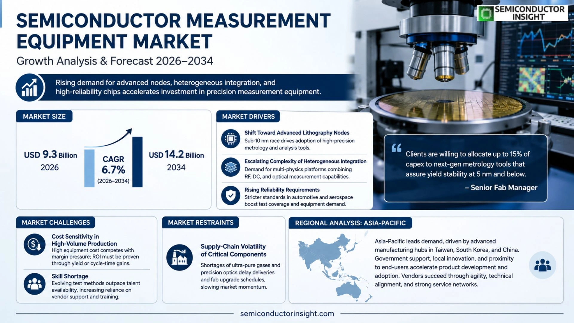
Semiconductor Measurement Equipment market size was valued at USD 8.5 billion in 2025. The market is projected to grow from USD 9.3 billion in 2026 to USD 14.2 billion by 2034, exhibiting a CAGR of 6.7% during the forecast period.
Semiconductor metrology devices are engineered for wafer‑level and thin‑film inspection after each processing step. Because modern nodes demand sub‑nanometer accuracy, these instruments provide high‑precision dimensional control, overlay measurement and defect detection essential for yield improvement.
The sector’s expansion is linked to rising demand for high‑performance computing, artificial‑intelligence accelerators, 5G infrastructure and electric‑vehicle electronics,all of which push manufacturers toward tighter process windows. Consequently, leading suppliers such as KLA, Applied Materials and Hitachi High‑Tech are accelerating R&D investments and expanding service networks across Asia‑Pacific where China mainland, Taiwan and South Korea together account for over 70% of sales.
MARKET DRIVERS
Shift Toward Advanced Lithography Nodes
Semiconductor Measurement Equipment Market is being pulled forward by manufacturers’ race to sub‑10 nm processes. As line widths shrink, traditional metrology tools lose resolution, prompting fabs to invest in high‑precision probers and scatter‑based analyzers. This transition raises equipment spend per wafer, reshaping vendor‑customer relationships and extending service contracts.
Escalating Complexity of Heterogeneous Integration
Chip‑stacking and system‑in‑package solutions compel designers to validate electrical continuity across disparate materials. Measurement platforms that combine RF, DC, and optical capabilities become essential, driving a broader portfolio demand across Semiconductor Measurement Equipment Market. Suppliers that can bundle these functions into a single workstation gain a competitive edge.
➤ “Clients are willing to allocate up to 15 % of capex to next‑gen metrology tools that assure yield stability at 5 nm and below,” notes a senior fab manager.
Beyond pure technology, regulatory pressure for higher reliability in automotive and aerospace chips forces manufacturers to adopt stricter test regimes, further inflating equipment purchases and service revenue streams.
MARKET CHALLENGES
Cost Sensitivity in High‑Volume Production
While cutting‑edge measurement tools unlock new design possibilities, their price tags remain a barrier for mid‑size fabs. Capital intensity competes with margin pressures, especially when yield improvements are incremental. Companies must justify spend through demonstrable reductions in scrap or cycle‑time.
Other Challenges
Skill Shortage
The rapid evolution of test methodologies outpaces the available talent pool. Operators need deep knowledge of nanometer‑scale physics, yet training programs lag, forcing firms to rely on vendor support contracts that add to total ownership cost.
MARKET RESTRAINTS
Supply‑Chain Volatility of Critical Components
Key consumables such as ultra‑pure gases and precision optics experience periodic shortages, inflating lead times for equipment delivery. When a fab’s upgrade schedule is delayed, the resulting idle capacity dampens overall market momentum, limiting immediate revenue spikes for equipment makers.
MARKET OPPORTUNITIES
AI‑Enabled Predictive Metrology
Machine‑learning algorithms that forecast process drift from real‑time sensor data are emerging as a high‑value add‑on. Vendors that embed AI analytics into their measurement suites can offer predictive maintenance and yield optimization as a service, opening recurring‑revenue models within Semiconductor Measurement Equipment Market.
Expansion into Emerging Applications
Quantum‑computing prototypes and mmWave 5G components require metrology beyond the scope of conventional tools. Companies that develop ultra‑low‑noise, high‑frequency probes stand to capture a niche yet growing segment, diversifying revenue beyond mainstream silicon production.
Semiconductor Measurement Equipment Market Trends
Escalating Precision Demands from Advanced Nodes
Semiconductor Measurement Equipment Market is feeling the pressure of sub‑10 nm production lines, where even nanometer‑scale variance can compromise yield. Manufacturers are investing in metrology tools that combine high‑resolution optics with real‑time data analytics, allowing wafer‑level adjustments without halting the fab. This shift is not merely technical; it translates into shorter ramp‑up times for new architectures and lower per‑unit defect costs. Asian powerhouses, which together command more than 70 % of semiconductor equipment sales, are spearheading collaborations that embed AI‑driven defect classification directly into inspection stations. For players outside the region, the imperative is to align product roadmaps with these precision‑first strategies or risk marginalisation as customers standardise on inline metrology solutions.
Other Trends
Optical Metrology Innovations
Recent advances in spectroscopic ellipsometry and scatterometry are reshaping the instrumentation landscape. By extending measurable wavelength ranges and improving signal‑to‑noise ratios, vendors are delivering devices capable of characterising both topography and material composition in a single pass. This convergence reduces capital expenditure for fabs that previously purchased separate tools for thickness and critical‑dimension assessment. Moreover, the enhanced throughput of these optical platforms dovetails with the surge in high‑performance compute workloads, where rapid feedback loops are essential to maintain production cadence. Companies that can package these capabilities with robust software ecosystems are likely to capture a larger slice of the market’s growth cycle.
Supply‑Chain Resilience and Pricing Dynamics
While demand for high‑precision measurement solutions climbs, Semiconductor Measurement Equipment Market faces headwinds from component shortages and fluctuating currency rates. The concentration of key optical and sensor components in a limited set of suppliers amplifies vulnerability, prompting manufacturers to diversify their supply bases and explore vertical integration. Pricing pressure is intensifying as end users negotiate longer service contracts that bundle hardware, software, and calibration services. Consequently, firms that can offer flexible financing models or performance‑based leasing are gaining competitive advantage. The strategic response to these constraints will shape investment decisions and dictate which players emerge as long‑term partners for semiconductor fabs worldwide.
COMPETITIVE LANDSCAPE
Key Industry Players
Semiconductor Measurement Equipment – Competitive Overview
KLA Corp. continues to dominate the measurement segment, leveraging an extensive portfolio that spans wafer‑level metrology, defect review and overlay solutions. Its ability to integrate hardware with advanced analytics has cemented long‑term contracts with the world’s leading fabs, translating into a clear revenue advantage. The market is heavily concentrated among three to four multinationals,KLA, Applied Materials, Hitachi High‑Tech and Nanometrics,each commanding double‑digit share across the global landscape. Their scale allows sustained investment in next‑generation platforms such as extreme‑ultraviolet (EUV) metrology, while a tier of specialist firms occupies the remaining space, addressing niche process nodes and application‑specific needs.
Beyond the tier‑1 tier, a cohort of focused players drives differentiation. Nova Measuring Instruments and Teradyne have sharpened their value proposition by targeting defect detection for advanced packaging and test‑in‑use scenarios. HEMMI SlideRule supplies high‑precision optical profilers that appeal to research‑intensive fabs, whereas Shanghai Precision Semiconductor Technology capitalizes on domestic demand in China’s rapidly expanding foundry base. Companies such as Advantest and Rudolph Technologies (now part of Ontic) extend their semiconductor test expertise into metrology, creating cross‑sell opportunities. This layered competitive environment forces incumbents to innovate continuously while offering smaller firms room to specialize in emerging process windows such as sub‑3 nm node verification.
List of Key Semiconductor Measurement Equipment Companies Profiled
- KLA Corp.
- Applied Materials Inc.
- Hitachi High‑Tech Corp.
- Nanometrics Inc.
- Nova Measuring Instruments Ltd.
- Teradyne Inc.
- Advantest Corp.
- HEMMI SlideRule
- Shanghai Precision Semiconductor Technology Co., Ltd.
- Rudolf Technologies (Ontic)
- QuesTek Innovations Ltd.
- Cambridge CMOS Sensors
Segment Analysis:
| Segment Category | Sub-Segments | Key Insights |
| By Type |
|
Optical Devices drive innovation in the measurement ecosystem because they enable sub‑nanometer resolution and non‑contact inspection, which is essential for next‑generation node scaling.
|
| By Application |
|
Front‑end measurement solutions are pivotal as device geometries shrink and multilayer stacks become more complex.
|
| By End User |
|
Integrated Device Manufacturers place the highest strategic emphasis on measurement equipment to safeguard product reliability across diverse application domains.
|
Regional Analysis: Semiconductor Measurement Equipment Market
Asia‑Pacific
The concentration of leading‑edge fabs in a handful of Asian cities concentrates purchase power, allowing equipment providers to negotiate multi‑plant agreements. This clustering also drives shared best practices, prompting suppliers to embed region‑specific calibration standards into their platforms.
Heavy investment in process research translates into frequent upgrades of measurement kits. Companies that co‑develop labs with semiconductor developers gain early access to emerging node requirements, fostering a pipeline of next‑generation metrology features.
Proximity to component suppliers shortens lead‑times for critical optics and sensors. Vendors exploit this by offering bundled solutions that embed diagnostic software, reducing integration risk for fab engineers.
National semiconductor roadmaps frequently earmark funds for precision equipment, encouraging manufacturers to align product roadmaps with policy milestones, thereby securing a stable order flow.
North America
North America remains a hub for design‑centric activities and niche test applications. Companies headquartered in the United States often emphasize modularity and software extensibility, catering to a client base that values flexibility over sheer volume. The region’s strong patent ecosystem incentivizes firms to differentiate through proprietary algorithms, while a mature aftermarket service culture sustains long‑term revenue streams. However, the comparatively higher cost structure limits the size of capital expenditures, nudging buyers toward leasing models and collaborative research agreements.
Europe
European manufacturers combine precision engineering heritage with a push toward sustainability. The emphasis on energy‑efficient instrumentation reflects broader regulatory trends, compelling suppliers to innovate in low‑power sensor design. Close ties between equipment firms and research consortia accelerate the adoption of standardized data formats, easing cross‑facility integration. While the market size is modest, the willingness to pay a premium for reliability and compliance makes Europe a profitable niche for high‑end metrology solutions.
South America
In South America, semiconductor activity clusters around a few emerging fabs and research parks. The market is driven more by incremental upgrades than by groundbreaking node transitions. Buyers prioritize cost‑effectiveness and robust after‑sales support, given the limited local servicing infrastructure. Partnerships with multinational vendors are common, allowing regional players to tap into global spare‑part networks while maintaining a degree of price sensitivity.
Middle East & Africa
The Middle East & Africa region exhibits a fledgling semiconductor footprint, yet investment in data‑center construction and IoT deployments sparks early demand for measurement equipment. Procurement decisions often hinge on turnkey solutions that bundle installation, training, and remote diagnostics. Local governments’ ambition to diversify economies creates opportunities for technology transfer programs, where equipment providers can embed knowledge‑sharing components into their contracts.
Report Scope
This market research report provides a comprehensive analysis of the Semiconductor Measurement Equipment Market , covering the forecast period 2026–2034. It offers detailed insights into market dynamics, technological advancements, competitive landscape, and key trends shaping the industry.
Key focus areas of the report include:
- Market Overview: The report begins with an overview outlining its current market scenario, key growth indicators, and industry transformation drivers. It discusses macroeconomic factors, demand–supply balance, regulatory landscape, and the strategic role of semiconductors in powering advancements across industries such as automotive, telecommunications, consumer electronics, and industrial automation.
- Market Size & Forecast: Historical data and future projections for revenue, unit shipments, and market value across major regions and segments.
- Segmentation Analysis: Detailed breakdown by product type, technology, application, and end-user industry to identify high-growth segments and investment opportunities.
- Regional Insights: Insights into market performance across North America, Europe, Asia-Pacific, Latin America, and the Middle East & Africa, including country-level analysis where relevant.
- Competitive Landscape: Profiles of leading market participants, including their product offerings, R&D focus, manufacturing capacity, pricing strategies, and recent developments such as mergers, acquisitions, and partnerships.
- Technology Trends & Innovation: Assessment of emerging technologies, integration of AI/IoT, semiconductor design trends, fabrication techniques, and evolving industry standards.
- Market Drivers & Restraints: Evaluation of factors driving market growth along with challenges, supply chain constraints, regulatory issues, and market-entry barriers.
- Stakeholder Insights: Insights for component suppliers, OEMs, system integrators, investors, and policymakers regarding the evolving ecosystem and strategic opportunities.
Primary and secondary research methods are employed, including interviews with industry experts, data from verified sources, and real-time market intelligence to ensure the accuracy and reliability of the insights presented.
FREQUENTLY ASKED QUESTIONS:
What is the current market size of Semiconductor Measurement Equipment Market?
-> Semiconductor Measurement Equipment market is projected to grow from USD 9.3 billion in 2026 to USD 14.2 billion by 2034, exhibiting a CAGR of 6.7%
Which key companies operate in Semiconductor Measurement Equipment Market?
-> Key players include KLA, Applied Materials, Hitachi High‑Tech, Nanometrics, Nova, Teradyne, Advantest, Spandnix, HEMMI Slide Rule, Shanghai Precision Semiconductor Technology, among others.
What are the key growth drivers?
-> Key growth drivers include high‑performance computing, artificial intelligence (AI), cloud computing, servers, 5G communications, and electric vehicles (EV).
Which region dominates the market?
-> Asia dominates, with China mainland, Taiwan, and South Korea together accounting for over 70% of global market share.
What are the emerging trends?
-> Emerging trends include the development of high‑precision semiconductor metrology instruments for wafer and thin‑film in‑line inspection, driven by ever‑shrinking device dimensions and stringent quality‑control requirements.

Get Sample Report PDF for Exclusive Insights
Report Sample Includes
- Table of Contents
- List of Tables & Figures
- Charts, Research Methodology, and more...
 Download Sample Report PDF