Semiconductor Abatement Equipment Market Insights
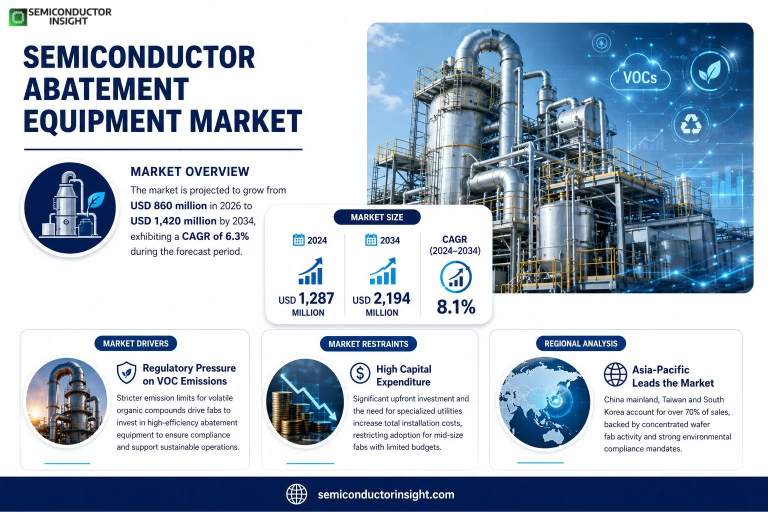
Semiconductor Abatement Equipment market was valued at USD 1287 million in 2024 and is projected to reach USD 2194 million by 2034, reflecting a compound annual growth rate of 8.1 % over the forecast horizon.
The equipment suite comprises thermal scrubbers, wet‑chemical reactors, catalytic converters and hybrid plasma‑wet systems designed to reduce hazardous semiconductor process gasessuch as fluorinated compounds, silane and phosphinebelow regulatory threshold limit values before atmospheric release.Growth is underpinned by expanding high‑performance computing demand, AI‑driven data centers and the rollout of 5G infrastructure, all of which intensify wafer‑fabrication activity. Regional concentration remains skewed toward East Asia, where China mainland, Taiwan and South Korea together command more than seventy percent of spend; meanwhile North America and Europe together account for roughly twenty‑three percent.
MARKET DRIVERS
Regulatory Pressure on VOC Emissions
fabs are tightening discharge limits for volatile organic compounds. Compliance requires high‑efficiency abatement units that can capture and neutralize emissions without compromising throughput. The shift reflects stricter national standards and the growing corporate focus on environmental stewardship, prompting equipment manufacturers to accelerate product roll‑outs.
Advances in Etching Technology
New plasma‑based etch processes generate finer features but also release more chemically aggressive by‑products. Chip makers therefore invest in next‑generation abatement systems that can handle higher acid concentrations while maintaining low pressure drop. This technical coupling fuels demand for equipment that can be integrated directly into existing process lines.
➤ Customers increasingly value modular designs that allow retrofitting without major plant shutdowns, creating a niche for flexible abatement solutions.
The convergence of tighter environmental rules and sophisticated etch chemistries is reshaping Semiconductor Abatement Equipment Market, encouraging OEMs to differentiate through energy‑saving designs and digital diagnostics that reduce operating costs.
MARKET CHALLENGES
Cost Sensitivity of Fab Operators
Capital budgets for new abatement units compete with investments in lithography and metrology. While compliance is non‑negotiable, fabs scrutinize total cost of ownership, favoring suppliers that can demonstrate lower lifecycle expenses through reduced reagent consumption and predictive maintenance.
Other Challenges
Supply Chain Volatility
Component shortages for critical scrubbers and catalyst materials have lengthened lead times. Manufacturers that maintain diversified sourcing or in‑house production of key parts gain a competitive edge, yet many smaller players struggle to assure timely delivery.
MARKET RESTRAINTS
High Capital Expenditure
Installation of full‑scale abatement plants often exceeds several million dollars, a figure that can delay project approvals, especially in regions where funding is tied to government incentives rather than internal cash flow.Beyond the upfront outlay, the need for specialized utilitiessuch as high‑purity water and dedicated exhaust ductsadds significant ancillary costs, limiting adoption among midsize fabs that operate on tighter margins.Financing structures for these projects remain fragmented; many equipment vendors still rely on traditional leasing models that do not fully align with the cash‑flow patterns of semiconductor manufacturers, creating a friction point for market expansion.
MARKET OPPORTUNITIES
Modular Retrofit Solutions
Older fabs seeking compliance without extensive downtime are turning to plug‑and‑play modules that can be inserted into existing ductwork. This approach shortens installation cycles and reduces disruption to high‑value wafer processing.Manufacturers that embed IoT sensors for real‑time performance monitoring can offer value‑added services, such as automated compliance reporting and predictive part replacement, opening new revenue streams beyond hardware sales.Emerging markets in Southeast Asia and Eastern Europe are scaling up semiconductor capacity under local environmental mandates, presenting a fertile ground for vendors that can deliver cost‑effective, scalable abatement platforms tailored to regional standards.
Semiconductor Abatement Equipment Market Trends
Regulatory Pressure Fuels Technology Adoption
The tightening of environmental legislation across major semiconductor hubs forces fabs to lower toxic gas emissions well beneath the legally defined thresholds. This constraint pushes equipment suppliers to refine thermal and wet scrubbers, as well as hybrid solutions capable of handling a broader spectrum of hazardous gases. Customers are increasingly willing to allocate budget toward abatement systems that guarantee compliance, because non‑conformity can halt production lines and attract hefty penalties. Consequently, Semiconductor Abatement Equipment Market sees a steady influx of new product releases that emphasize reliability, lower operating costs, and modular designs that can be retrofitted to older process chambers.
Other Trends
Technology Diversification Across Process Segments
Manufacturers are expanding their portfolios beyond traditional combustion‑wash units to include dry catalytic converters and plasma‑enhanced wet modules. Each technology aligns with a specific process needfor example, plasma‑wet systems are gaining acceptance in etch and deposition steps where moisture‑sensitive reactions dominate. The diversification mitigates the risk of a single‑point failure in a fab’s abatement line and enables operators to tailor solutions to the exact chemical profile of their workloads. By offering interchangeable modules, vendors create a value proposition that appeals to both greenfield fabs and those undertaking capacity upgrades.
Regional Realignment of Supply Chains
Asia continues to dominate the semiconductor ecosystem, accounting for over 70 % of equipment purchases, with China, Taiwan, and South Korea leading the charge. The concentration has prompted Western distributors to reassess logistics and inventory strategies, especially as geopolitical considerations introduce new compliance checkpoints. In North America and Europe, where the combined share hovers around 23 %, end‑users are favoring local service partners that can provide rapid spare‑part turnaround and on‑site technical support. This shift encourages a broader network of regional assembly facilities, reducing lead times and enhancing resilience against cross‑border disruptions.
COMPETITIVE LANDSCAPE
Key Industry Players
Semiconductor Abatement Equipment: Competitive Overview 2024‑2034
Ebara remains the most visible contender, leveraging a portfolio that couples thermal combustion units with catalytic scrubbers. Its presence across North America, Europe and Asia gives it a leverage point in supplying multinational fabs that must meet strict TLV limits. The market shows a dual‑tier architecture: a handful of vertically integrated manufacturers dominate the high‑capacity segment, while a crowded fringe of specialists supplies niche treatment technologies such as plasma‑wet or combined wet‑dry systems. This separation creates clear entry barriers for new entrants that lack deep engineering expertise or service networks.Beyond the leader, a constellation of focused firms shapes the competitive dynamics. Busch Vacuum Solutions and Standard Technology (GST) concentrate on modular wet‑type abatement units that cater to mid‑size foundries, whereas Edwards Vacuum and CS Clean Solutions specialize in dry‑type solutions for high‑purity environments. Niche innovators like DAS Environmental Expert, Highvac and Ecosys Abatement drive incremental improvements in energy efficiency, while industrial conglomerates such as Atlas Copco (CSK), Nippon Sanso and Showa Denko extend their gas‑handling expertise into the abatement arena. European and Japanese giants Air Liquide and Linde bring advanced catalytic chemistries, reinforcing the regional diversification of supplier capabilities.
List of Key Semiconductor Abatement Equipment Companies Profiled
- Ebara
- Busch Vacuum Solutions
- Standard Technology (GST)
- Edwards Vacuum
- CS Clean Solutions
- DAS Environmental Expert
- Atlas Copco (CSK)
- Ecosys Abatement
- Highvac
- Nippon Sanso
- Showa Denko
- Air Liquide
- Linde
- Entegris
- Veolia Water Technologies
Segment Analysis:
| Segment Category | Sub-Segments | Key Insights |
| By Type |
|
Combustion‑wash is often the leading segment because it directly addresses high‑energy gases with reliable thermal breakdown.
|
| By Application |
|
Plasma Etching emerges as the dominant application segment.
|
| By End User |
|
Semiconductor fabs lead this dimension.
|
| By Treatment Technology |
|
Hybrid solutions are gaining traction.
|
| By Regulatory Driver |
|
Environmental emission limits drive market dynamics.
|
Regional Analysis: Semiconductor Abatement Equipment Market
North America
Federal and state agencies have expanded permissible emission limits, compelling fab operators to replace older abatement units with more selective systems. Incentives for low‑carbon technologies further accelerate adoption, while audit penalties tighten the cost of non‑compliance.
Recent disruptions have prompted customers to diversify suppliers, favoring vendors that can guarantee on‑time delivery of critical components such as catalyst cartridges and sensor modules, thereby reducing inventory risk.
The market sees a shift toward plasma‑based abatement and nanofiber filtration, technologies that deliver higher removal efficiency while consuming less power, aligning with operators’ cost‑optimization goals.
Large integrated device manufacturers dominate procurement, yet emerging fabless firms are increasingly sourcing boutique abatement solutions to meet niche process requirements, expanding the overall addressable base.
Europe
European nations combine stringent EU directives with national green‑transition agendas, compelling semiconductor players to prioritize solvent recovery and acid neutralization. Companies operating in Germany and the Netherlands often integrate digital twins of their abatement trains, enabling predictive maintenance and reducing downtime. The appetite for circular‑economy practices means vendors that can demonstrate closed‑loop material cycles gain a competitive edge, especially in markets where carbon pricing is already embedded in operating models. This regulatory and cultural environment nurtures collaboration between equipment makers and research institutes, accelerating the rollout of low‑temperature catalytic processes that align with Europe’s broader sustainability targets.
Asia‑Pacific
The Asia‑Pacific region presents a paradox of rapid fab expansion paired with fragmented regulatory oversight. While China, Taiwan, and South Korea invest heavily in new capacity, local standards for emissions vary widely, creating pockets where legacy abatement equipment persists. Multinational suppliers leverage this heterogeneity by offering scalable kits that can be upgraded as jurisdictions tighten rules. Moreover, the region’s cost‑sensitive operators value solutions that deliver high removal efficiency with a modest capital outlay, prompting a surge in modular scrubber designs. Competitive pressure among fabs also drives early adoption of water‑reuse technologies, positioning the Asia‑Pacific market as a testbed for innovative abatement cycles.
South America
In South America, modest fab activity is concentrated in Brazil and Mexico, where emerging environmental legislation is beginning to influence procurement decisions. Operators face the dual challenge of meeting local compliance while contending with limited import pipelines for advanced equipment. This has encouraged partnerships with regional engineering firms that can assemble hybrid abatement units using locally sourced components. The market’s slower pace allows vendors to pilot pilot‑scale trials of next‑generation solvent capture systems, providing a proving ground that could later inform larger deployments as the continent’s semiconductor footprint expands.
Middle East & Africa
The Middle East & Africa region remains nascent in semiconductor manufacturing, yet rising interest in downstream electronics assembly creates ancillary demand for abatement solutions. Countries such as the United Arab Emirates are establishing free‑zone facilities that require strict emissions controls to attract foreign investors. Meanwhile, Africa’s limited industrial base means that equipment providers often bundle abatement kits with broader utility‑management packages, emphasizing reliability under high ambient temperatures. Strategic positioning of service hubs in this region allows vendors to respond swiftly to the few yet high‑visibility projects that emerge, laying the groundwork for future market depth.
Report Scope
This market research report provides a comprehensive analysis of the Semiconductor Abatement Equipment Market , covering the forecast period 2026–2034. It offers detailed insights into market dynamics, technological advancements, competitive landscape, and key trends shaping the industry.
Key focus areas of the report include:
- Market Overview: The report begins with an overview outlining its current market scenario, key growth indicators, and industry transformation drivers. It discusses macroeconomic factors, demand–supply balance, regulatory landscape, and the strategic role of semiconductors in powering advancements across industries such as automotive, telecommunications, consumer electronics, and industrial automation.
- Market Size & Forecast: Historical data and future projections for revenue, unit shipments, and market value across major regions and segments.
- Segmentation Analysis: Detailed breakdown by product type, technology, application, and end-user industry to identify high-growth segments and investment opportunities.
- Regional Insights: Insights into market performance across North America, Europe, Asia-Pacific, Latin America, and the Middle East & Africa, including country-level analysis where relevant.
- Competitive Landscape: Profiles of leading market participants, including their product offerings, R&D focus, manufacturing capacity, pricing strategies, and recent developments such as mergers, acquisitions, and partnerships.
- Technology Trends & Innovation: Assessment of emerging technologies, integration of AI/IoT, semiconductor design trends, fabrication techniques, and evolving industry standards.
- Market Drivers & Restraints: Evaluation of factors driving market growth along with challenges, supply chain constraints, regulatory issues, and market-entry barriers.
- Stakeholder Insights: Insights for component suppliers, OEMs, system integrators, investors, and policymakers regarding the evolving ecosystem and strategic opportunities.
Primary and secondary research methods are employed, including interviews with industry experts, data from verified sources, and real-time market intelligence to ensure the accuracy and reliability of the insights presented.
FREQUENTLY ASKED QUESTIONS:
What is the current market size of Semiconductor Abatement Equipment Market?
-> Semiconductor Abatement Equipment Market was valued at USD 1,287 million in 2024 and is expected to reach USD 2,194 million by 2034, growing at a CAGR of 8.1% over the forecast period.
Which key companies operate in Semiconductor Abatement Equipment Market?
-> Key players include Ebara, Busch Vacuum Solutions, GST ( Standard Technology), Edwards Vacuum, CS Clean Solutions, DAS Environmental Expert, CSK (Atlas Copco), Ecosys Abatement, Highvac, Nippon Sanso, and Showa Denko.
What are the key growth drivers?
-> Key growth drivers include high‑performance computing, artificial intelligence, cloud computing, servers, 5G networks, and electric vehicles (EV), all of which increase demand for semiconductor manufacturing and consequently for abatement solutions.
Which region dominates the market?
-> Asia dominates the market, with China mainland, Taiwan and South Korea together accounting for over 70% of Semiconductor Abatement Equipment sales.
What are the emerging trends?
-> Emerging trends feature the adoption of diverse abatement technologies such as thermal (combustion‑wash), wet, catalytic and plasma‑wet processes to meet tighter environmental regulations and enable a greener semiconductor production environment.
Get Sample Report PDF for Exclusive Insights
Report Sample Includes
- Table of Contents
- List of Tables & Figures
- Charts, Research Methodology, and more...
 Download Sample Report PDF