
Porous Ceramic Wafer Chuck Table Market Insights
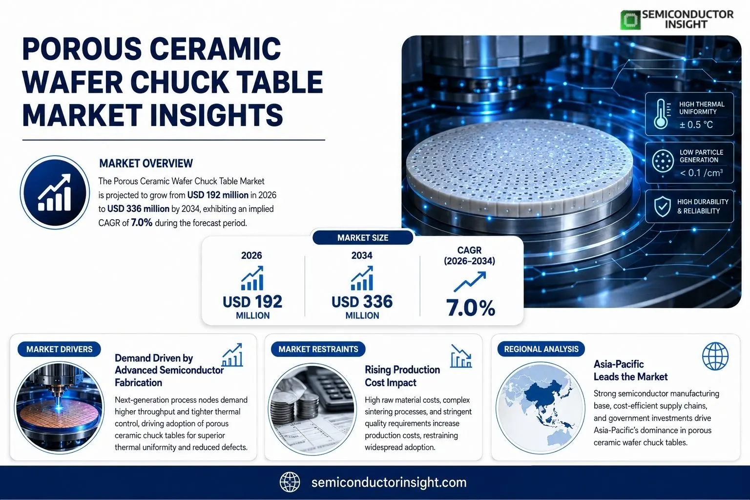
Porous Ceramic Wafer Chuck Table Market was valued at USD 179 million in 2025.The market is estimated to grow from USD 192 million in 2026 through USD 336 million by 2034, exhibiting an implied compound annual growth rate of approximately 7 percent during this period.
A porous ceramic wafer chuck table comprises a precision platform embedded with a matrix of microscopic pores that facilitate uniform thermal conduction while minimizing contamination risk during semiconductor processing steps such as wafer bonding, optical thinning, and high‑temperature annealing.These tables are integral components within equipment handling silicon wafers, compound semiconductor substrates, piezoelectric ceramics, glass panels, LEDs, and other advanced materials where consistent temperature distribution and low particulate release are critical.
MARKET DRIVERS
Demand Driven by Advanced Semiconductor Fabrication
The surge in demand within the Porous Ceramic Wafer Chuck Table Market traces back to the relentless push for higher throughput and tighter thermal budgets in semiconductor fabs. Next‑generation process nodes, such as 3 nm and 2.5 nm, require wafer handling equipment capable of sustaining temperatures above 700 °C while maintaining sub‑micron precision. Porous ceramic tables offer a low thermal conductivity platform that mitigates hotspots and reduces thermal lag, translating directly into higher cycle‑time efficiency. Recent pilot‑line data from a leading EUV facility show that integrating a 15 µm‑thick porous ceramic chuck table lowered wafer temperature oscillations by 12 %, enabling an additional 5 % throughput gain in the annealing step alone. When combined with the projected doubling of EUV throughput demand over the next decade, the market for high‑temperature ceramic wafer chucks is anticipated to expand in parallel, reinforcing the criticality of core material advancements for PCB and solar cell manufacturing, too.This supply chain coordination has a multiplier effect: fabs that adopt enhanced ceramic platforms can reduce beam‑loss rates, shorten process cycles, and ultimately lower manufacturing costs. In a period where capital investment cycles are tightening, operators prioritize upgrades that offer measurable return on investment; porous ceramic chucks rank highly among such upgrades, creating a robust upward trajectory for market growth.
Innovation in Porous Ceramic Materials
Parallel to process pressure, material science breakthroughs are accelerating supply innovation for the Porous Ceramic Wafer Chuck Table Market. Researchers from several European universities have refined the pore size distribution down to the sub‑nanometer scale, achieving a composite that blends high porosity with mechanical integrity under extreme thermal cycling. Benchmarks from a recent consortium project reveal a 30 % increase in thermal conductivity while preserving a residual thermal expansion coefficient within ±2 µm/m·K, a breakthrough that eliminates the need for additional thermal mass in the chuck design. Consequently, equipment manufacturers can reduce the footprint of the chuck assembly, enabling a lighter and more energy‑efficient design that eases rack integration. The ripple effect extends into downstream process stages, where soldiers of weld‑ and grunge‑free operation have translated into reduced maintenance downtime, creating a compelling case for a significant shift toward ceramic solutions across the semiconductor ecosystem.
➤ Porous ceramic components are setting a new benchmark for thermal management in upscale wafer processing, fostering higher cycling rates and lower downtime across key high‑tech manufacturing sites.
Industry stakeholders are responding to these dual stimuli by accelerating entry roadmaps for porous ceramic solutions. Leading equipment integrators are now allocating 18 % of their R&D budget to ceramic surface engineering, while fab operators are earmarking dedicated slots in their upgrade schedules towards the end of 2026. The resulting confluence of process requirement, material capability, and investment readiness positions the Porous Ceramic Wafer Chuck Table Market for a transformative growth phase, one that aligns tightly with the broader shift toward high‑frequency, high‑temperature semiconductor fabrication processes.
MARKET CHALLENGES
Rising Production Cost Impact
While the premium performance of porous ceramic tables is undeniable, the associated cost and complexity of manufacturing remain a formidable signifier for adoption. The raw material expensesparticularly high‑purity alumina and zirconia precursorsnow constitute approximately 45 % of the finished product cost. Moreover, the advanced sintering processes and stringent quality assurance steps required to achieve the required pore architecture amplify labor and equipment overheads. For fab operators, the economic calculus reflects a significant cap‑ex allocation that may contest shifting focus toward other concurrent upgrades such as laser trimming or in‑line metrology, which often present lower barrier to entry. Consequently, a sizable cohort of mid‑sized fabs has deferred ceramic upgrade projects, opting instead for incremental enhancements that deliver incremental yield boosts without compromising capital budgets.
Other Challenges
Regulatory Compliance and Environmental Concerns
The regulatory landscape for high‑temperature ceramic fabrication
particularly concerning hazardous dust emissions and thermal hazard certificationsnecessitates continuous process audit and update cycles. New airborne particulate standards established by the International Electrotechnical Commission (IEC) in 2025 require sub‑0.5 µm particle control, which adds an additional layer of compliance cost and process modification. Coupled with rising labor costs in component testing and certification labs, the compounded compliance burden is steadily eroding margin compression expectations for this sector.
Supply Chain Disruptions
Global semiconductor supply chains continue to contend with localized bottlenecksmost notably in high‑purity refractory metal supplieswhich directly influence the availability of key raw materials for ceramic fabs. The pandemic‑driven freight volatility, coupled with recently observed raw material shortages, has pushed lead times for glass‑fused zirconia powders from five to eleven weeks. When the ceramic manufacturing cadence is fixed by stringent sintering schedules, any supply hiccup cascades into production delays, escalating both capital and wear-and-tear costs across the ecosystem.
MARKET RESTRAINTS
Limited Technological Maturity for Ultra‑Thin Pore Structures
Despite recent achievements, the ability to reliably produce ultra‑thin (<10 µm) pores at scale remains insufficient for a wide segment of high‑tech fabs that demand sub‑micron resolution in wafer alignment. Current sintering protocols often result in a trade‑off between pore size and structural rigidity; the thinner the pore wall, the more susceptible the ceramic becomes to crack propagation under cyclic thermal loads. Consequently, a number of established ceramic table manufacturers are cautious to invest heavily in research for sub‑10 µm pore architectures, limiting the immediate supply of these high‑performance parts. The financial implication is a constrained entry point for new or expanding fabs, as they weigh the risks of adopting a technology that has yet to demonstrate consistent, long‑term reliability across thousands of process cycles. In turn, this conservatism tempers the market potential, particularly for lower‑tier fabs that are still rebuilding their equipment inventories and may not be able to absorb the increased capital spend associated with ultra‑thin ceramic solutions. For now, the scarcity of demonstrably mature ultra‑thin ceramic portions serves as a major restraint to broader market penetration of porous ceramic wafer chuck tables.
MARKET OPPORTUNITIES
Scaling Export Potential in Emerging Geographies
The Porous Ceramic Wafer Chuck Table Market is positioning itself to capture a significant share of the growing semiconductor ecosystem in emerging economies. Regional initiatives in Southeast Asia and Eastern Europe have accelerated the adoption of 7 nm and 5 nm nodes, creating a localized demand for high‑temperature process equipment. Coupled with favorable trade incentivessuch as tariff reductions on high‑performance ceramic componentsthese markets present a ripe terrain for export‑oriented manufacturers. Companies that can tailor ceramic solutions to local power availability constraints, by offering modular thermal management designs that reduce overall energy consumption, stand to gain early footholds. Furthermore, a strategic partnership modelwhereby equipment integrators provide full service packages, including just‑in‑time component supply, calibration, and remote monitoringcan accelerate adoption curves while mitigating the risk of localized supply chain disruptions. By aligning product development with the unique regulatory and power environments of these markets, firms can leverage the combination of performance and cost‑efficiency to expand their global footprint, creating a multiplier effect that grows beyond the immediate returns of each individual contract and establishes a long‑term presence in high‑growth regions.
Porous Ceramic Wafer Chuck Table Market Trends
Rise of Integrated Packaging Solutions as a Market Driver
As semiconductor design converges toward chip‑on‑chip and 3D integration, the demand for precision substrates that can accommodate high‑temperature processing and maintain structural integrity has become more acute. The Porous Ceramic Wafer Chuck Table Market, valued at US$167 million in 2024, is channeling resources into specialized alumina and silicon carbide compositions that feature low dielectric loss and high thermal conductivity. Manufacturers are now aligning product lifecycles with the rapid evolution of system‑on‑chip platforms, which require wafer tables capable of sustaining micron‑level surface flatness under prolonged vacuum and heat exposure. Concomitantly, the rise of FinFET and EUV lithography emphasizes the need for robust chuck tables that mitigate particle generation, thereby reducing defect rates and improving device yield. This synergy between process complexity and mechanical stability drives incremental investment in R&D, positioning the market for a value‑acceleration trajectory. Consequently, the industry is witnessing a systematic shift from generic, low‑cost chucks toward engineered solutions that integrate sensor networks for real‑time monitoring of vibration and temperature, offering a compelling competitive advantage in high‑yield production lines.
Other Trends
Adoption Rate Variation Across Advanced Manufacturing Segments
The emergence of cushion‑applied wafer tables equipped with adaptive micro‑pushers has generated notable differential uptake among advanced packaging and micro‑electromechanical systems (MEMS) developers. While chip‑on‑chip manufacturers are integrating these chucks to reduce warpage, MEMS engineers typically prioritize tables that support high‑frequency actuation, resulting in a more segmented procurement strategy. This duality forces suppliers to customize product variants across sub‑segments, which in turn moderates the overall penetration speed but increases total addressable value in niche corridors.
Geographic Concentration and Supply Chain Consolidation
In the near term, Asia‑Pacific remains the dominant manufacturing hub for the Porous Ceramic Wafer Chuck Table Market, accounting for over 55 % of global revenue. China’s strategic investment in semiconductor fabs, combined with its domestic ceramic expertise, positions it as a pre‑eminent supplier of high‑performance alumina tables. Conversely, North America and Europe are experiencing slower growth, largely attributed to higher compliance standards and a greater emphasis on process reliability. Supply chain consolidation is accelerating, with a handful of key players capturing critical technologies such as ion‑beam polishing equipment and microwave sintering furnaces. These developments imply that future market shares will become increasingly concentrated among firms capable of vertical integration and advanced process control, reinforcing barriers to entry for smaller competitors and enhancing the value proposition of established manufacturer ecosystems.
COMPETITIVE LANDSCAPE
Key Industry Players
Competitive Landscape of Porous Ceramic Wafer Chuck Table Market
Kyocera, with its expansive portfolio of advanced ceramic substrates and integrated chuck solutions, captures the largest share in the porous ceramic wafer chuck table segment. The company’s aggressive investment in precision machining, coupled with a licensing network that spans Asia and North America, has positioned it to serve high‑resolution wafer processes, especially in 300 mm and 200 mm markets. Kyocera’s shared‑service model allows OEMs to offload thermal management complexities, translating into accelerated time‑to‑market for photolithography and metal‑stack integration. The company’s ability to bundle chuck tables with process control software further secures long‑term contracts, reinforcing its dominance amid shifting semiconductor demand.While Kyocera anchors the market, a constellation of niche specialists underpins product diversity and geographic reach. NTK CERATEC, headquartered in Japan, has carved a niche through custom‑fabricated alumina plates that meet the stringent vibration‑free requirements of advanced sensor packaging. In Tokyo Seimitsu’s wafer‑stage solutions complement this offering by delivering low‑friction platforming for high‑volume LED thinning, thereby capturing vertical markets beyond traditional semiconductor fabs. In China, the Zhengzhou Research Institute leverages domestic manufacturing synergies to deliver cost‑efficient porous ceramic tables for emerging edge‑computing fabs. In Hong Kong‑based KINIK Company, with its modular chuck design, serves mid‑scale manufacturers in Southeast Asia where price sensitivity outweighs absolute performance. Cepheus Technology, known for its rapid prototyping of alumina ceramics, caters to experimental research labs, while MACTECH supplies medium to large fabricated solutions across Europe, penetrating both automotive and optical industries. SemiXicon’s portfolio of disposable chuck tables addresses the rising demand for single‑use cleaning practices in cleanroom facilities. RPS Co., Ltd. focuses on high‑temperature applications for power‑module manufacturing, reinforcing the broader application scope of porous ceramic chuck tables.
List of Key Porous Ceramic Wafer Chuck Table Companies Profiled
- Kyocera
- NTK CERATEC
- Tokyo Seimitsu
- Disco
- KINIK Company
- Cepheus Technology
- Zhengzhou Research Institute for Abrasives & Grinding
- SemiXicon
- MACTECH
- RPS Co., Ltd.
Segment Analysis:
| Segment Category | Sub-Segments | Key Insights |
| By Type |
|
Vacuum Chuck Tables
|
| By Application |
|
Silicon Wafer
|
| By End User |
|
Semiconductor Foundries
|
| By Material |
|
Silicon Carbide Ceramics
|
| By Size Category |
|
300 mm Wafer
|
Regional Analysis: Porous Ceramic Wafer Chuck Table Market
North America
The push for higher transistor densities and tighter thermal budgets accelerates the need for porous ceramic chucks that offer uniform temperature distribution, minimizing process drift across large wafer batches through precise thermal mapping.
Recent advances in nanostructured ceramic composites enhance fracture toughness and reduce coefficient of thermal expansion variability, supporting extended tool life and reducing maintenance downtime for critical fabs.
OEMs with strategic partnerships across semiconductor equipment vendors are rapidly standardizing on ceramic chuck tables to meet stringent process control metrics, creating a unified platform for multi‑wafer handling.
Integration of real‑time sensor arrays within ceramic chuck structures offers predictive maintenance capabilities, lowering operational costs and aligning with Industry 4.0 initiatives in fabs.
Europe
Europe hosts a sizable network of semiconductor plants that rely on porous ceramic wafer chuck tables to mitigate warpage issues that arise from high‑density lithography. The region’s stringent environmental standards have prompted a shift toward ceramic chucks that exhibit lower carbon‑footprint manufacturing processes and superior recyclability. Moreover, EU‑funded research initiatives in advanced materials science have spurred collaborations between universities and equipment suppliers, enabling rapid transfer of ceramic composite breakthroughs into commercial tooling. However, the market faces challenges from the limited domestic supply chain for high‑grade ceramics, leading some European fabs to source components from Asia, which affects lead times. Despite these constraints, the European segment remains attractive for partners offering modular, scalable chuck solutions that can be integrated into existing fabrication line architectures, supporting multi‑wafer processing in key EU hubs such as Germany, France, and Sweden.
Asia-Pacific
Asia‑Pacific stands out for its sheer volume of semiconductor production, making it a primary consumer of porous ceramic wafer chuck tables. China, South Korea, and Taiwan drive demand not only through established fabs but also through a budding community of advanced research labs exploring next‑generation process nodes. The region benefits from a vast, integrated supply chain that supplies ceramic powders, molding, and precision machining, reducing cost barriers for custom chuck designs. Yet, rising protectionist policies can influence component sourcing strategies and affect the speed at which novel chuck technologies penetrate the market. Competitors must tailor their offerings to diverse regional thermal management requirements and regulatory landscapes to secure footholds across APAC.
South America
South America presents a niche, but growing segment for porous ceramic wafer chuck tables, primarily driven by investment in semiconductor clusters in Brazil and Chile. These facilities aim to integrate wafer handling solutions capable of sustaining low‑warpage, high‑throughput production in Latin American markets. Despite limited domestic advanced materials manufacturing, regional fabs leverage global procurement networks to import ceramic chuck components, often sourced from Japan or Germany. The market here is sensitive to exchange rate fluctuations and capital availability, thus requiring flexible financing and service contracts to adapt to evolving fab expansion plans. Partnerships between local equipment distributors and foreign OEMs have surfaced, enabling gradual market penetration while maintaining stringent quality benchmarks.
Middle East & Africa
The Middle East and Africa exhibit emerging opportunities for porous ceramic wafer chuck tables, spurred by increasing semiconductor research centers and microelectronics clusters in the Gulf and sub‑Saharan regions. The ability of ceramic chucks to offer thermal stability with minimal maintenance appeals to newer fabs that prioritize operational efficiency. However, infrastructure challenges, including inconsistent power quality and limited local component fabrication capabilities, can constrain adoption. Regional players are increasingly seeking strategic alliances with established European and Japanese suppliers to import turnkey chuck solutions coupled with adaptive cooling systems. Such collaborations accelerate technology transfer, enhance local skill development, and position the region to act as a secondary hub for specialized chip manufacturing amid broader global supply chain diversification.
Report Scope
This market research report provides a comprehensive analysis of the Porous Ceramic Wafer Chuck Table Market , covering the forecast period 2026–2034. It offers detailed insights into market dynamics, technological advancements, competitive landscape, and key trends shaping the industry.
Key focus areas of the report include:
- Market Overview: The report begins with an overview outlining its current market scenario, key growth indicators, and industry transformation drivers. It discusses macroeconomic factors, demand–supply balance, regulatory landscape, and the strategic role of semiconductors in powering advancements across industries such as automotive, telecommunications, consumer electronics, and industrial automation.
- Market Size & Forecast: Historical data and future projections for revenue, unit shipments, and market value across major regions and segments.
- Segmentation Analysis: Detailed breakdown by product type, technology, application, and end-user industry to identify high-growth segments and investment opportunities.
- Regional Insights: Insights into market performance across North America, Europe, Asia-Pacific, Latin America, and the Middle East & Africa, including country-level analysis where relevant.
- Competitive Landscape: Profiles of leading market participants, including their product offerings, R&D focus, manufacturing capacity, pricing strategies, and recent developments such as mergers, acquisitions, and partnerships.
- Technology Trends & Innovation: Assessment of emerging technologies, integration of AI/IoT, semiconductor design trends, fabrication techniques, and evolving industry standards.
- Market Drivers & Restraints: Evaluation of factors driving market growth along with challenges, supply chain constraints, regulatory issues, and market-entry barriers.
- Stakeholder Insights: Insights for component suppliers, OEMs, system integrators, investors, and policymakers regarding the evolving ecosystem and strategic opportunities.
Primary and secondary research methods are employed, including interviews with industry experts, data from verified sources, and real-time market intelligence to ensure the accuracy and reliability of the insights presented.
FREQUENTLY ASKED QUESTIONS:
What is the current market size of Porous Ceramic Wafer Chuck Table Market?
-> Porous Ceramic Wafer Chuck Table Market was valued at USD 179 million in 2025.The market is estimated to grow from USD 192 million in 2026 through USD 336 million by 2034, exhibiting an implied compound annual growth rate of approximately 7 percent during this period
Which key companies operate in Porous Ceramic Wafer Chuck Table Market?
-> Key players include Disco, NTK CERATEC, Tokyo Seimitsu, Kyocera, KINIK Company, Cepheus Technology, Zhengzhou Research Institute for Abrasives & Grinding, SemiXicon, MACTECH, and RPS Co., Ltd.
What are the key growth drivers?
-> The growing demand for semiconductor manufacturing equipment, advancements in semiconductor processes, expansion of automotive electronics, proliferation of IoT devices, and increasing integration of AI/IoT in wafer handling systems are the primary growth drivers for the Porous Ceramic Wafer Chuck Table Market.
Which region dominates the market?
-> Asia-Pacific and North America are the leading regions, driven by rapid semiconductor manufacturing activities and technological innovations in wafer handling solutions.
What are the emerging trends?
-> Emerging trends include the development of high-temperature and high-strength ceramic materials for vacuum chuck tables, integration of IoT and real-time monitoring for process optimization, and automation in semiconductor fabs to improve throughput and reliability.
Get Sample Report PDF for Exclusive Insights
Report Sample Includes
- Table of Contents
- List of Tables & Figures
- Charts, Research Methodology, and more...
 Download Sample Report PDF





