Physical Layer Chip Market Insights
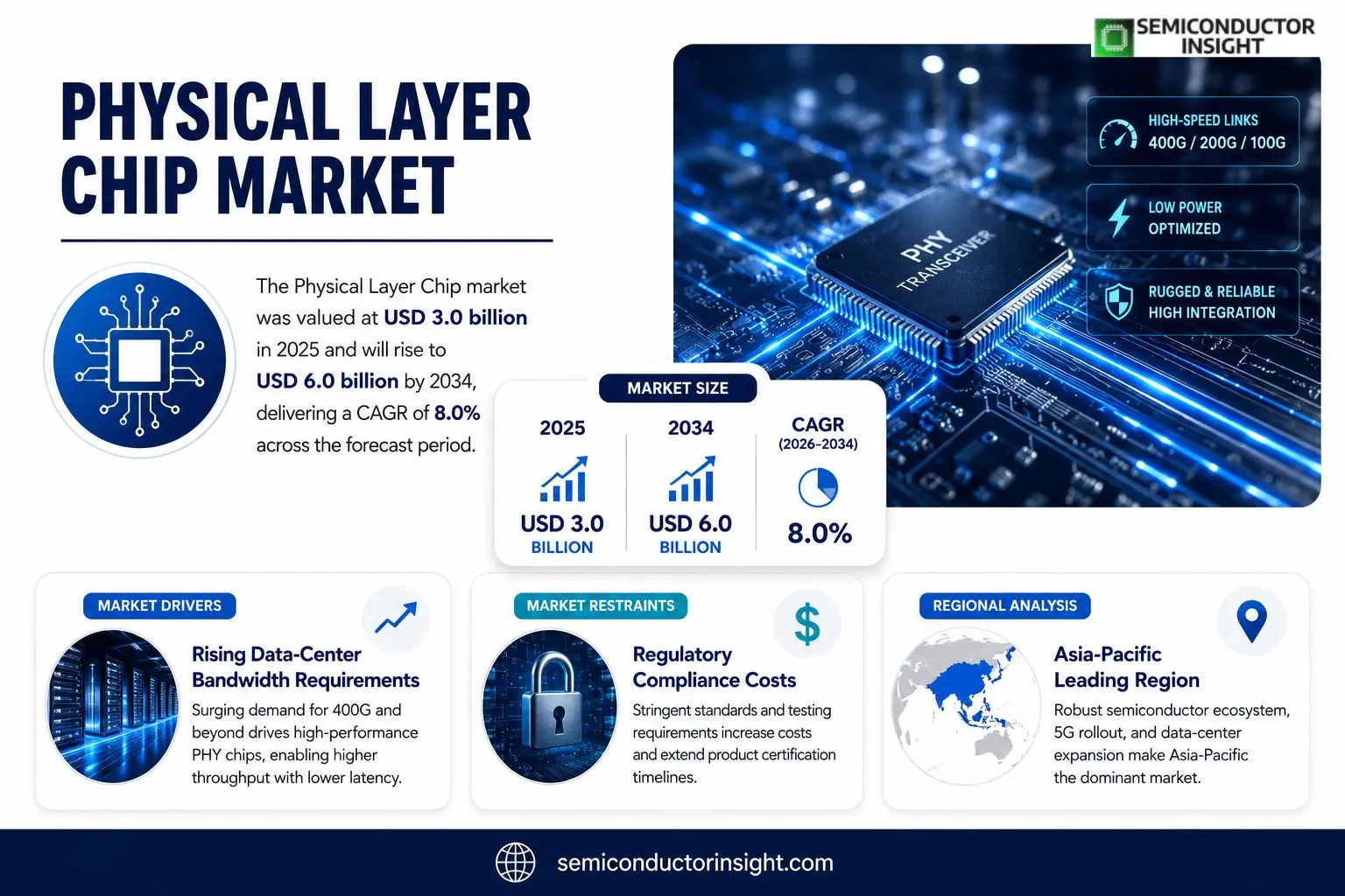
Physical Layer Chip market size was valued at USD 3.0 billion in 2025 and will rise to USD 6.0 billion by 2034, delivering a CAGR of 8.0 % across the forecast horizon.
Physical layer chips comprise transceiver modules and PHY integrated circuits that translate digital data into electrical or optical signals for standards such as Ethernet‑10G, ‑25G‑40G, ‑100G and beyond. These components sit at OSI layer 1, handling signal conditioning, clock recovery and line‑code conversion essential for high‑speed networking equipment.The sector gains momentum because data‑center expansion, cloud‑edge convergence and rollout of next‑generation mobile networks increase demand for higher bandwidth links. Moreover, cost‑effective silicon photonics integration reduces power consumption while supporting multi‑lane architectures. Leading suppliersincluding Broadcom, Marvell Technology Group, Intel’s Fulcrum division and NXP Semiconductorshave announced new multi‑rate PHY families targeting routers and switches, reinforcing competitive pressure.
MARKET DRIVERS
Rising Data‑Center Bandwidth Requirements
Enterprises are upgrading inter‑server links to support 400 Gb/s and beyond, compelling silicon designers to push signalling integrity limits. This shift raises the demand for high‑precision transceivers, which sit at the core of Physical Layer Chip Market. Manufacturers that can deliver lower jitter and tighter eye‑diagram margins are seeing accelerated order books.
Adoption of Advanced Manufacturing Nodes
Foundries moving to 12 nm and finer geometries enable chip‑scale integration of analog front‑ends with digital controllers, shrinking bill of materials and power envelopes. Companies that realign their product roadmaps to these nodes report cost‑per‑bit reductions of up to 15 %, a persuasive value proposition for OEMs.
➤ Clients that pair silicon‑photonic modules with next‑gen PHY chips are achieving 20 % higher data‑center throughput without additional cooling infrastructure.
These forces together create a virtuous cycle: higher bandwidth pushes deeper silicon, which in turn expands the addressable market for bespoke PHY solutions, reinforcing growth momentum for the sector.
MARKET CHALLENGES
Escalating Design Complexity
Designers now juggle simultaneous constraintssignal integrity, power delivery, and thermal managementwithin a single die. The learning curve for integrating multi‑protocol support (e.g., Ethernet, PCIe, and CPRI) prolongs development cycles, throttling time‑to‑market for newcomers.
Other Challenges
Supply‑Chain Volatility
Fluctuating silicon wafer yields and geopolitical tensions have introduced lead‑time uncertainty, prompting OEMs to hold larger inventory buffers and eroding cash flow efficiency.
Talent Shortage
The niche expertise required for analog‑mixed‑signal layout remains scarce, driving up labor rates and limiting the capacity of smaller fabs to scale production.
MARKET RESTRAINTS
Regulatory Compliance Costs
Stringent emissions and safety standards across regions compel chip makers to invest in additional testing cycles, inflating unit costs by an estimated 8 %.Furthermore, the requirement to certify compliance for each protocol version adds procedural overhead, which can deter rapid iteration of new features.These compliance hurdles, while essential for market access, temper the upside for firms lacking robust validation infrastructure.
MARKET OPPORTUNITIES
Emergence of 5G and Edge Computing
Deployments of private 5G networks and edge nodes require compact, low‑latency transceivers that operate across a wider frequency spectrum. Vendors that engineer PHY chips with built‑in adaptive equalization stand to capture a sizable share of this nascent demand.In parallel, the automotive sector’s shift toward vehicle‑to‑everything (V2X) communications demands ruggedized physical‑layer solutions capable of withstanding harsh environments, opening a vertical with projected multi‑billion‑dollar revenue potential.Strategic partnerships between silicon vendors and system integrators can accelerate time‑to‑market for these use cases, converting technical advantage into measurable market share.
Physical Layer Chip Market Trends
Shift Toward Higher‑Speed Interfaces
Physical Layer Chip Market is witnessing a decisive move to faster serial standards such as 25 Gb, 40 Gb, and 100 Gb Ethernet. Manufacturers are re‑engineering transceiver architectures to accommodate tighter eye‑diagram margins while preserving power efficiency. This engineering pressure stems from data‑center operators seeking to double host‑to‑host bandwidth without expanding rack footprint. Consequently, design houses are favoring silicon‑photonic integration and advanced equalization techniques, which in turn raise the bar for component suppliers that must meet stricter jitter and loss‑budget requirements. The practical up‑shot for vendors is an accelerated product‑development cycle and a greater emphasis on intellectual‑property licensing rather than purely volume‑driven sales.
Other Trends
Emergence of 100G and Above Solutions
Beyond the 100 Gb threshold, the market is experimenting with 200 Gb and 400 Gb lanes aimed at hyperscale cloud backbones. The push is not merely about raw speed; it reflects a strategic effort to reduce the number of active lanes per chassis, thereby cutting cooling and power overhead. Early adopters report that consolidating lane count translates into measurable OPEX savings, prompting a ripple effect through the supply chain. Chipmakers that can deliver robust signal‑integrity across longer reaches without resorting to excessive amplification will secure a competitive edge in this nascent segment.
Regional Demand Divergence
While North America and Europe remain strong adopters of 25 Gb and 100 Gb modules for enterprise networking, Asia‑Pacific shows a faster uptake of 10 Gb solutions driven by telecom operators upgrading legacy transport networks. The disparity is rooted in differing investment cycles: mature markets are replacing aging infrastructure, whereas emerging regions prioritize cost‑effective upgrades that align with localized rollout plans. This split creates a bifurcated sales landscape where high‑margin, high‑performance chips dominate western portfolios, while volume‑oriented, price‑sensitive designs fuel growth in the east. Companies that calibrate product mixes to these regional preferences can better manage inventory risk and capture marginal gains across Physical Layer Chip Market.
COMPETITIVE LANDSCAPEKey Industry Players
Physical Layer Chip Market Competitive Overview
Broadcom remains the de‑facto leader in the physical‑layer semiconductor segment, leveraging its extensive portfolio of 10 G to 400 G transceiver IP and a robust manufacturing footprint across Asia and the United States. The company’s strategic acquisitionsmost notably the purchase of Broadcom’s 100 G silicon‑photonic assetshave deepened its foothold in data‑center and carrier‑grade networking equipment. By consolidating design, silicon, and test capabilities, Broadcom can offer customers a one‑stop solution that compresses time‑to‑market and lowers total cost of ownership, a decisive advantage in an ecosystem where OEMs demand both speed and reliability. Cisco, while traditionally known for networking hardware, increasingly influences the physical‑layer market through its in‑house silicon development and close collaboration with fabless partners, shaping product roadmaps that prioritize high‑density, power‑efficient PHYs for cloud infrastructure.Beyond the tier‑one giants, a cadre of specialized firms sustains competitive pressure and fuels innovation. Marvell’s aggressive push into 400 G Ethernet PHYs has forced incumbents to accelerate their own high‑speed offerings, while Intel’s Fulcrum line provides a unique combination of programmable logic and fixed‑function blocks that appeal to hyperscale operators seeking flexibility. NXP and Infineon each exploit automotive‑grade reliability to capture a growing share of vehicle‑to‑infrastructure connectivity. Smaller yet technically agile players such as IC Plus, Centec Networks and Ethernity Networks focus on niche marketsindustrial IoT, edge routing, and low‑latency crypto offloadwhere bespoke PHY features command premium pricing. The diversity of business models, from vertically integrated fabs to fabless design‑only outfits, creates a fragmented but vibrant competitive tapestry that demands constant strategic recalibration from all participants.
List of Key Physical Layer Chip Companies Profiled
- Broadcom Inc.
- Cisco Systems, Inc.
- Marvell Technology Group Ltd.
- Intel Corporation (Fulcrum)
- NXP Semiconductors N.V.
- Infineon Technologies AG
- Microchip Technology Inc.
- Fujitsu Limited
- VIA Technologies, Inc.
- IC Plus Corp.
- Centec Networks, Inc.
- Ethernity Networks, Inc.
- Qualcomm Inc.
- Texas Instruments Inc.
Segment Analysis:
| Segment Category | Sub-Segments | Key Insights |
| By Type |
|
High‑Speed Ethernet continues to dominate innovation cycles.
|
| By Application |
|
Data‑Center Switching drives the most compelling adoption patterns.
|
| By End User |
|
Data Center Operators shape the strategic roadmap for Physical Layer chips.
|
| By Speed Tier |
|
High‑Speed Tier emerges as the primary growth driver.
|
| By Integration Level |
|
Fully Integrated ASICs are gaining strategic importance.
|
Regional Analysis: Physical Layer Chip Market
Asia‑Pacific
The bulk of wafer production resides in Taiwan’s Hsinchu Science Park and South Korea’s Gyeonggi cluster, where economies of scale lower per‑unit costs for high‑frequency layers. This geographic density fuels rapid iteration cycles, allowing design houses to test new materials without long lead times.
Regional design firms are pioneering silicon‑photonic co‑integration, blending optical and electrical pathways on a single die. The push stems from data‑center operators seeking bandwidth beyond the limits of copper interconnects.
Multi‑tiered supplier networks across Japan, Singapore, and Malaysia provide redundancy for critical substrates, insulating end‑users from single‑source disruptions that have plagued other semiconductor segments.
Governments are harmonizing electromagnetic‑compatibility standards, which eases cross‑border certification for chips destined for 5G base stations and automotive radar systems.
North America
North America remains a significant demand engine for Physical Layer Chip Market, driven primarily by the United States’ data‑center expansion and the automotive push toward advanced driver‑assistance systems. Companies such as NVIDIA and Intel are investing heavily in ultra‑low‑latency transceiver solutions to support the migration to cloud‑native networking. Although the region does not host many front‑end fabs, it excels in R&D, especially in silicon‑photonic design, creating a robust upstream ecosystem that feeds global manufacturers. Regulatory clarity around spectrum allocation for mmWave applications adds confidence for suppliers targeting 5G and upcoming 6G trials.
Europe
European stakeholders focus on sustainability and energy‑efficient interconnects, reflecting the bloc’s broader climate agenda. Initiatives like the European Chips Act fund projects that embed low‑power physical layer circuits into industrial IoT devices. Germany’s automotive giants are collaborating with chip designers to embed high‑precision clock distribution networks, a prerequisite for vehicle‑to‑infrastructure communication. While fab capacity is limited, strong design expertise and a network of specialty foundries in the Netherlands and France sustain a niche yet influential market segment.
South America
In South America, Physical Layer Chip Market is shaped by a gradual rollout of 5G services in Brazil, Chile, and Colombia. Telecom operators are upgrading backhaul links, prompting a modest uptick in demand for high‑frequency front‑end modules. Local distributors act as critical intermediaries, customizing solutions to meet diverse climate and regulatory conditions across the continent. Although the region lacks manufacturing depth, partnerships with Asian suppliers are expanding, allowing it to benefit from cost‑effective sourcing while building technical competence locally.
Middle East & Africa
The Middle East & Africa segment is propelled by significant infrastructure investments in smart‑city projects and oil‑field communications. Nations such as Saudi Arabia and United Arab Emirates are establishing data‑center corridors that require resilient, high‑throughput physical layer components. Meanwhile, African telecoms are deploying rural broadband, where ruggedized chipsets can tolerate harsh environments. The market is primarily import‑driven, yet local value‑addition is emerging through assembly and testing facilities that cater to regional standards and reduce lead times for end‑users.
Report Scope
This market research report provides a comprehensive analysis of the Physical Layer Chip Market , covering the forecast period 2026–2034. It offers detailed insights into market dynamics, technological advancements, competitive landscape, and key trends shaping the industry.
Key focus areas of the report include:
- Market Overview: The report begins with an overview outlining its current market scenario, key growth indicators, and industry transformation drivers. It discusses macroeconomic factors, demand–supply balance, regulatory landscape, and the strategic role of semiconductors in powering advancements across industries such as automotive, telecommunications, consumer electronics, and industrial automation.
- Market Size & Forecast: Historical data and future projections for revenue, unit shipments, and market value across major regions and segments.
- Segmentation Analysis: Detailed breakdown by product type, technology, application, and end-user industry to identify high-growth segments and investment opportunities.
- Regional Insights: Insights into market performance across North America, Europe, Asia-Pacific, Latin America, and the Middle East & Africa, including country-level analysis where relevant.
- Competitive Landscape: Profiles of leading market participants, including their product offerings, R&D focus, manufacturing capacity, pricing strategies, and recent developments such as mergers, acquisitions, and partnerships.
- Technology Trends & Innovation: Assessment of emerging technologies, integration of AI/IoT, semiconductor design trends, fabrication techniques, and evolving industry standards.
- Market Drivers & Restraints: Evaluation of factors driving market growth along with challenges, supply chain constraints, regulatory issues, and market-entry barriers.
- Stakeholder Insights: Insights for component suppliers, OEMs, system integrators, investors, and policymakers regarding the evolving ecosystem and strategic opportunities.
Primary and secondary research methods are employed, including interviews with industry experts, data from verified sources, and real-time market intelligence to ensure the accuracy and reliability of the insights presented.
FREQUENTLY ASKED QUESTIONS:
What is the current market size of Physical Layer Chip Market?
-> Physical Layer Chip Market was valued at USD million in 2025 and is expected to reach USD million by 2034.
Which key companies operate in Physical Layer Chip Market?
-> Key players include Axalta Coating Systems, AkzoNobel, BASF SE, PPG, Sherwin-Williams, and 3M, among others.
What are the key growth drivers?
-> Key growth drivers include railway infrastructure investments, urbanization, and demand for durable coatings.
Which region dominates the market?
-> Asia-Pacific is the fastest-growing region, while Europe remains a dominant market.
What are the emerging trends?
-> Emerging trends include bio-based coatings, smart coatings, and sustainable rail solutions.
Get Sample Report PDF for Exclusive Insights
Report Sample Includes
- Table of Contents
- List of Tables & Figures
- Charts, Research Methodology, and more...
 Download Sample Report PDF