PCB for Semiconductor Market Insights
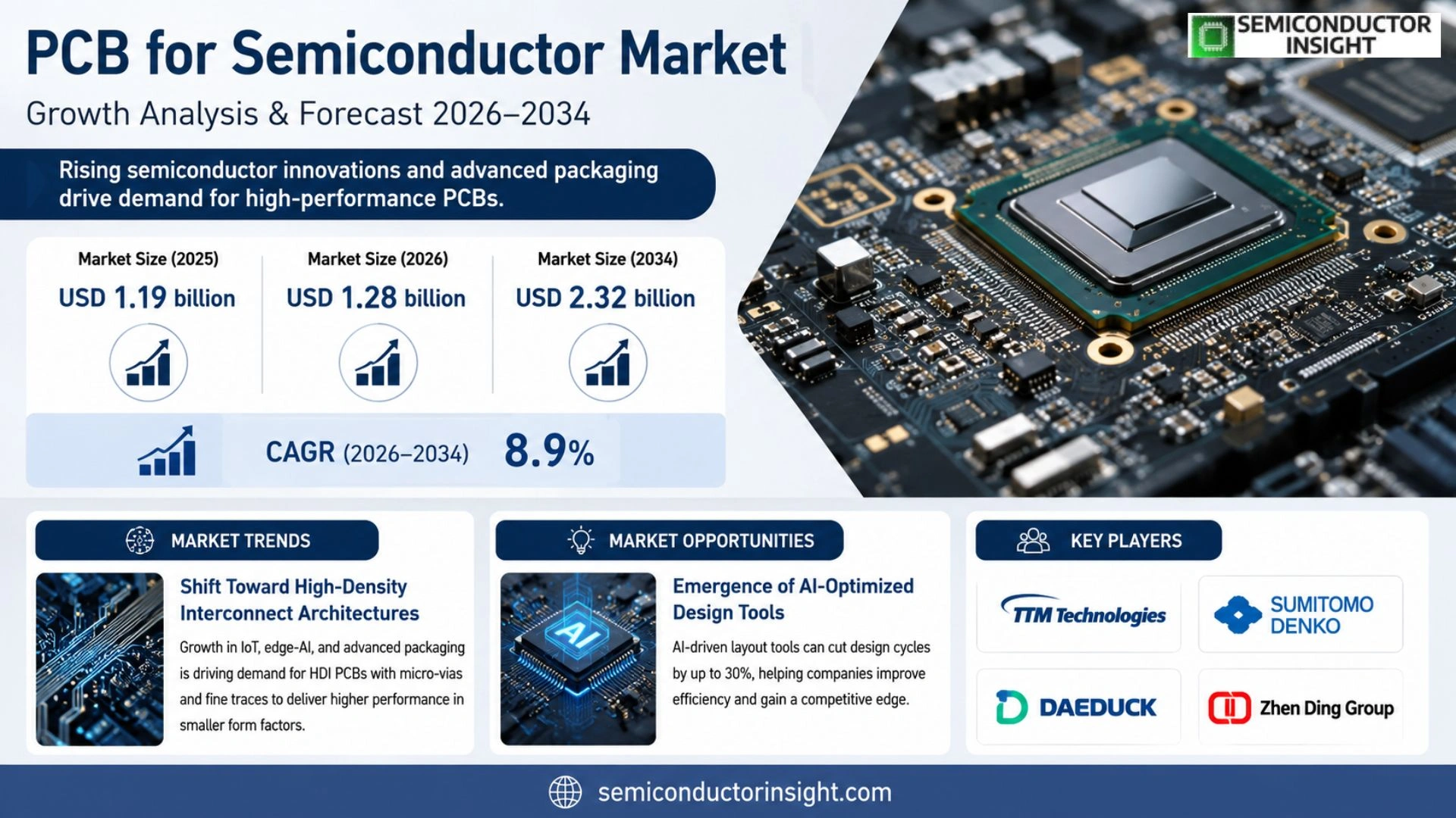
PCB for Semiconductor market size was valued at USD 1.19 billion in 2025. The market is projected to grow from USD 1.28 billion in 2026 to USD 2.32 billion by 2034, exhibiting a CAGR of 8.9% during the forecast period.
PCB for Semiconductor refers to high‑performance printed circuit boards engineered specifically to host semiconductor devices such as ASICs, power modules, and mixed‑signal chips. These boards combine precise impedance control, advanced material stacks (e.g., BT resin or ceramic substrates), and fine‑line routing to meet the thermal‑mechanical demands of modern silicon technologies.
The sector is expanding because semiconductor manufacturers are scaling production of AI accelerators, automotive power electronics, and IoT modules,all of which require reliable high‑frequency interconnects. Moreover, recent collaborations,such as TTM Technologies partnering with a leading fabless chip designer on next‑generation load boards,illustrate how ecosystem players are accelerating innovation pipelines. Key participants include TTM Technologies, Sumitomo Denko, Daeduck Group, Zhen Ding Group, Unimicron, DSBJ, Millennium Circuits Limited, Tripod, IBIDEN CO and MEIKO ELECTRONICS Co.
MARKET DRIVERS
Advanced Packaging Requirements
The rise of heterogeneous integration forces chip manufacturers to adopt multilayer PCBs that can accommodate finer trace widths and tighter tolerances. Design flexibility becomes a decisive factor as customers seek to embed power‑management, RF, and digital functions within a single board, thereby shortening the overall product development cycle.
Shift Toward Miniaturization
Portable devices, wearables, and IoT sensors demand ever‑smaller form factors. By leveraging high‑density interconnect (HDI) technologies, PCB for Semiconductor Market enables a reduction in board size without sacrificing signal integrity. Cost efficiency emerges because fewer discrete components are required, allowing manufacturers to consolidate bill‑of‑materials.
➤ “Supply chains that can deliver sub‑milimeter copper features within 10‑week lead times are now a competitive advantage.”
Regulatory pressure for higher reliability, especially in automotive and aerospace, pushes suppliers to certify their processes to stringent standards. Firms that demonstrate compliance can command premium pricing, reinforcing investment in next‑generation laminate materials and automated fabrication lines.
MARKET CHALLENGES
Escalating Material Costs
Fluctuations in copper and specialty resin prices erode profit margins for PCB producers. When raw‑material costs rise 12‑15 % year‑over‑year, manufacturers are forced to either absorb the expense or pass it to downstream chipmakers, which can stall volume growth.
Other Challenges
Skill Shortage in Advanced Manufacturing
The transition to micro‑via and buried‑layer processes requires a workforce proficient in laser drilling and precision lamination. Training pipelines have not kept pace, leading to bottlenecks that delay order fulfillment and increase lead times.
MARKET RESTRAINTS
Regulatory Compliance Overheads
Stringent environmental directives, such as RoHS and REACH, impose costly testing regimes on PCB suppliers. Small‑batch producers, in particular, struggle to allocate resources for continuous compliance monitoring, limiting their ability to serve niche segments of PCB for Semiconductor Market.
Additionally, the certification process for high‑frequency boards can take up to six months, discouraging rapid entry of new players and concentrating market power among established vendors.
MARKET OPPORTUNITIES
Emergence of AI‑Optimized Design Tools
Artificial‑intelligence‑driven layout engines can automatically optimize trace routing for impedance matching and thermal distribution. Early adopters of these tools are reporting design‑cycle reductions of up to 30 %, opening a clear advantage for firms that integrate AI into their PCB for Semiconductor Market offerings.
Furthermore, the growing demand for edge‑computing platforms creates a niche for ruggedized boards capable of operating in extreme temperatures. Companies that develop high‑temperature laminate families stand to capture a segment that is currently underserved.
PCB for Semiconductor Market Trends
Shift Toward High‑Density Interconnect Architectures
The semiconductor ecosystem is demanding ever‑smaller footprints while maintaining signal integrity, prompting PCB manufacturers to adopt high‑density interconnect (HDI) techniques. Designers are layering micro‑vias and fine traces to accommodate advanced packages such as fan‑out wafer‑level and 2.5‑D/3‑D ICs. This engineering pressure originates from the surge in IoT endpoints and edge‑AI devices, where processing capability must be squeezed into constrained form factors. For PCB suppliers, the transition translates into higher material costs for copper‑clad laminates and tighter tolerances in fabrication, but it also unlocks premium pricing opportunities. Companies that have invested in automated optical inspection and laser drilling are better positioned to capture the value chain shift, while laggards risk margin compression as buyers migrate to more capable vendors.
Other Trends
Emergence of Flexible PCB Solutions for Automotive and Wearables
Automotive electrification and the proliferation of wearable health monitors are driving demand for flexible substrates that can endure vibration, temperature cycles, and repeated bending. Flexible PCBs enable designers to route circuits around irregular chassis shapes, reducing assembly steps and weight. Consequently, material suppliers are expanding polyimide and liquid‑crystal polymer offerings, while contract manufacturers are scaling roll‑to‑roll production lines. The strategic implication for market participants is a need to diversify product portfolios; firms that continue to focus solely on rigid boards may miss out on a growing revenue stream that is expected to command a larger share of PCB for Semiconductor Market in the next five years.
Regional Diversification of Production Capacity
Asia continues to host the bulk of fabrication capacity, yet recent announcements from North‑American and European players indicate a deliberate move to localize critical supply nodes. Geopolitical tensions and component shortages have exposed the vulnerability of overly centralized supply chains. By establishing “near‑shore” production hubs in the United States, Germany, and Israel, manufacturers aim to shorten lead times for high‑mix, low‑volume orders typical of prototype and small‑batch semiconductor projects. This geographic rebalancing creates competitive pressure on legacy Asian fabs to improve service levels and invest in advanced process control. For end‑users, the shift promises greater resilience and the ability to align procurement strategies with regional compliance frameworks, thereby influencing long‑term partnership decisions within PCB for Semiconductor Market.
COMPETITIVE LANDSCAPE
Key Industry Players
PCB for Semiconductor Competitive Overview – 2024 – 2031
TTM Technologies dominates the high‑mix, high‑volume segment of PCB for Semiconductor arena, leveraging its global fab network and deep engineering expertise. The company’s ability to co‑ship multilayer rigid and flexible boards with embedded passive components has secured long‑term contracts with leading foundries in the United States, Taiwan, and Europe. This sizeable footprint forces smaller outfits to concentrate on niche applications or regional customers, reinforcing a tiered structure where a handful of integrated manufacturers set pricing baselines while a broader ecosystem of specialized suppliers fills product‑specific gaps.
Beyond the market leader, a constellation of firms sustains competitive pressure. Sumitomo Denko focuses on high‑frequency ceramic‑based substrates, capitalising on Japan’s automotive and 5G rollout. Daeduck Group and Zhen Ding Group excel in precision probe‑card production for advanced logic testing, while Unimicron and DSBJ command substantial share in load‑board and burn‑in board markets across Asia. Millennium Circuits Limited, Tripod Technology, and MEIKO ELECTRONICS Co differentiate through flexible‑circuit capabilities that address IoT and wearable modules. IBIDEN CO, Nippon Mektron, and Kyocera diversify with hybrid material stacks that improve thermal performance. Shinko Electric, Camtek, and ASE Technology Holding round out the landscape, each pursuing strategic acquisitions to broaden portfolio breadth and geographic reach.
List of Key PCB for Semiconductor Companies Profiled
- TTM Technologies
- Sumitomo Denko
- Daeduck Group
- Zhen Ding Group
- Unimicron
- DSBJ
- Millennium Circuits Limited
- Tripod Technology
- IBIDEN CO
- MEIKO ELECTRONICS Co
- Nippon Mektron
- Kyocera
- Shinko Electric
- Camtek
- ASE Technology Holding
Segment Analysis:
| Segment Category | Sub-Segments | Key Insights |
| By Type |
|
Rigid PCB dominates the market due to its proven reliability and mechanical stability.
Flexible PCB is gaining traction for emerging form‑factor applications.
|
| By Application |
|
Load Board serves as the primary interface for wafer‑level testing, delivering high‑precision signal integrity.
Probe Card is essential for probing semiconductor dice during test phases.
Burn‑In Board underpins reliability assurance for power and automotive chips.
|
| By End User |
|
Electronics Manufacturers continue to rely on robust PCB solutions for mainstream semiconductor products.
IoT Device Makers push for flexible and miniaturized PCB formats to embed advanced processors.
Automotive Electronics prioritize high‑reliability PCBs for power‑train and ADAS modules.
|
| By Material |
|
FR‑4 remains the workhorse material for standard semiconductor PCBs.
Polyimide is favored for flexible and high‑temperature applications.
Rogers (High‑Frequency) caters to advanced RF and microwave semiconductor segments.
|
| By Technology |
|
High‑Density Interconnect (HDI) is essential for stacking and miniaturizing semiconductor packages.
Embedded Passives integrate resistors, capacitors, and inductors within PCB layers.
Micro‑Via Technologies provide reliable interlayer connectivity for high‑performance chips.
|
Regional Analysis: PCB for Semiconductor Market
Recent expansions in Shenzhen and Suwon have lifted overall throughput, enabling the region to absorb spikes from the automotive and 5G segments without compromising lead times. Capacity buffers are now measured in weeks rather than days, a strategic shift that reduces the risk of order‑backlog overruns.
Diversification of raw‑material sources, especially copper foil and high‑frequency laminates, has lowered exposure to single‑point failures. Collaborative logistics platforms that share real‑time inventory data further insulate manufacturers from port‑level disruptions.
R&D clusters in Tokyo and Hsinchu are experimenting with embedded passive components, a trend that promises to shrink board footprints and shorten signal paths,attributes prized by next‑generation processors.
Harmonized environmental standards across ASEAN have simplified compliance, while regional intellectual‑property frameworks give multinational designers confidence to co‑develop advanced multilayer stacks.
North America
North America maintains a sophisticated design ecosystem that values precision and fast prototyping. Companies in the United States and Canada often source high‑frequency laminates from niche suppliers to meet stringent signal‑integrity specifications demanded by data‑center processors. Although labor costs are higher, the region offsets this through automation and a strong emphasis on sustainable manufacturing practices, which resonate with OEMs pursuing green‑technology roadmaps. The strategic focus here is on value‑added services,such as embedded testing and customized stack‑up engineering,that differentiate suppliers beyond raw cost metrics.
Europe
European players differentiate themselves through rigorous quality regimes and compliance with the EU’s stricter waste‑reduction directives. Nations such as Germany and the Netherlands have cultivated clusters where PCB fabrication dovetails with semiconductor R&D, creating a feedback loop that shortens time‑to‑market for specialty applications like autonomous‑vehicle controllers. While the market size lags behind Asia‑Pacific, the emphasis on reliability and traceability commands premium pricing, attracting OEMs that need certified supply chains for safety‑critical systems.
South America
South America is emerging as a cost‑effective alternative for mid‑volume production, especially in Brazil and Argentina where labor pools are expanding and governmental incentives target high‑tech manufacturing. Local firms are increasingly adopting Industry 4.0 tools to improve yield, yet they still rely on imported high‑frequency materials, which introduces a dependency that could constrain rapid scaling. Nevertheless, the region’s growing consumer‑electronics demand provides a steady base for incremental capacity upgrades.
Middle East & Africa
The Middle East & Africa region is still in the early stages of PCB for Semiconductor development, but investment plans announced by Gulf sovereign wealth funds signal a willingness to build advanced fabrication footprints. Early adopters in the United Arab Emirates are focusing on aerospace and defense projects that require rugged, high‑temperature boards. Africa’s contribution remains modest, with a handful of niche players serving local telecom infrastructure. The overarching narrative is one of nascent capability coupled with strategic intent to capture downstream semiconductor assembly work.
Report Scope
This market research report provides a comprehensive analysis of the PCB for Semiconductor Market , covering the forecast period 2026–2034. It offers detailed insights into market dynamics, technological advancements, competitive landscape, and key trends shaping the industry.
Key focus areas of the report include:
- Market Overview: The report begins with an overview outlining its current market scenario, key growth indicators, and industry transformation drivers. It discusses macroeconomic factors, demand–supply balance, regulatory landscape, and the strategic role of semiconductors in powering advancements across industries such as automotive, telecommunications, consumer electronics, and industrial automation.
- Market Size & Forecast: Historical data and future projections for revenue, unit shipments, and market value across major regions and segments.
- Segmentation Analysis: Detailed breakdown by product type, technology, application, and end-user industry to identify high-growth segments and investment opportunities.
- Regional Insights: Insights into market performance across North America, Europe, Asia-Pacific, Latin America, and the Middle East & Africa, including country-level analysis where relevant.
- Competitive Landscape: Profiles of leading market participants, including their product offerings, R&D focus, manufacturing capacity, pricing strategies, and recent developments such as mergers, acquisitions, and partnerships.
- Technology Trends & Innovation: Assessment of emerging technologies, integration of AI/IoT, semiconductor design trends, fabrication techniques, and evolving industry standards.
- Market Drivers & Restraints: Evaluation of factors driving market growth along with challenges, supply chain constraints, regulatory issues, and market-entry barriers.
- Stakeholder Insights: Insights for component suppliers, OEMs, system integrators, investors, and policymakers regarding the evolving ecosystem and strategic opportunities.
Primary and secondary research methods are employed, including interviews with industry experts, data from verified sources, and real-time market intelligence to ensure the accuracy and reliability of the insights presented.
FREQUENTLY ASKED QUESTIONS:
What is the current market size of PCB for Semiconductor Market?
-> PCB for Semiconductor market is projected to grow from USD 1.28 billion in 2026 to USD 2.32 billion by 2034, exhibiting a CAGR of 8.9%
Which key companies operate in PCB for Semiconductor Market?
-> Key players include TTM Technologies, Sumitomo Denko, Daeduck Group, Zhen Ding Group, Unimicron, DSBJ, Millennium Circuits Limited, Tripod, IBIDEN CO, MEIKO ELECTRONICS Co.
What are the key growth drivers?
-> Key growth drivers include increasing demand for high‑performance semiconductor PCBs, growth of IoT devices, expansion of data‑center infrastructure, and rising adoption of advanced packaging technologies.
Which region dominates the market?
-> Asia holds the largest share, driven by strong manufacturing ecosystems in China, Japan, and South Korea, while North America shows rapid growth in advanced applications.
What are the emerging trends?
-> Emerging trends include flexible and rigid‑flex hybrid PCBs, miniaturization of load boards, integration of AI‑enabled testing solutions, and increased focus on sustainable materials.

Get Sample Report PDF for Exclusive Insights
Report Sample Includes
- Table of Contents
- List of Tables & Figures
- Charts, Research Methodology, and more...
 Download Sample Report PDF