
Package Warpage Control Material Market Insights
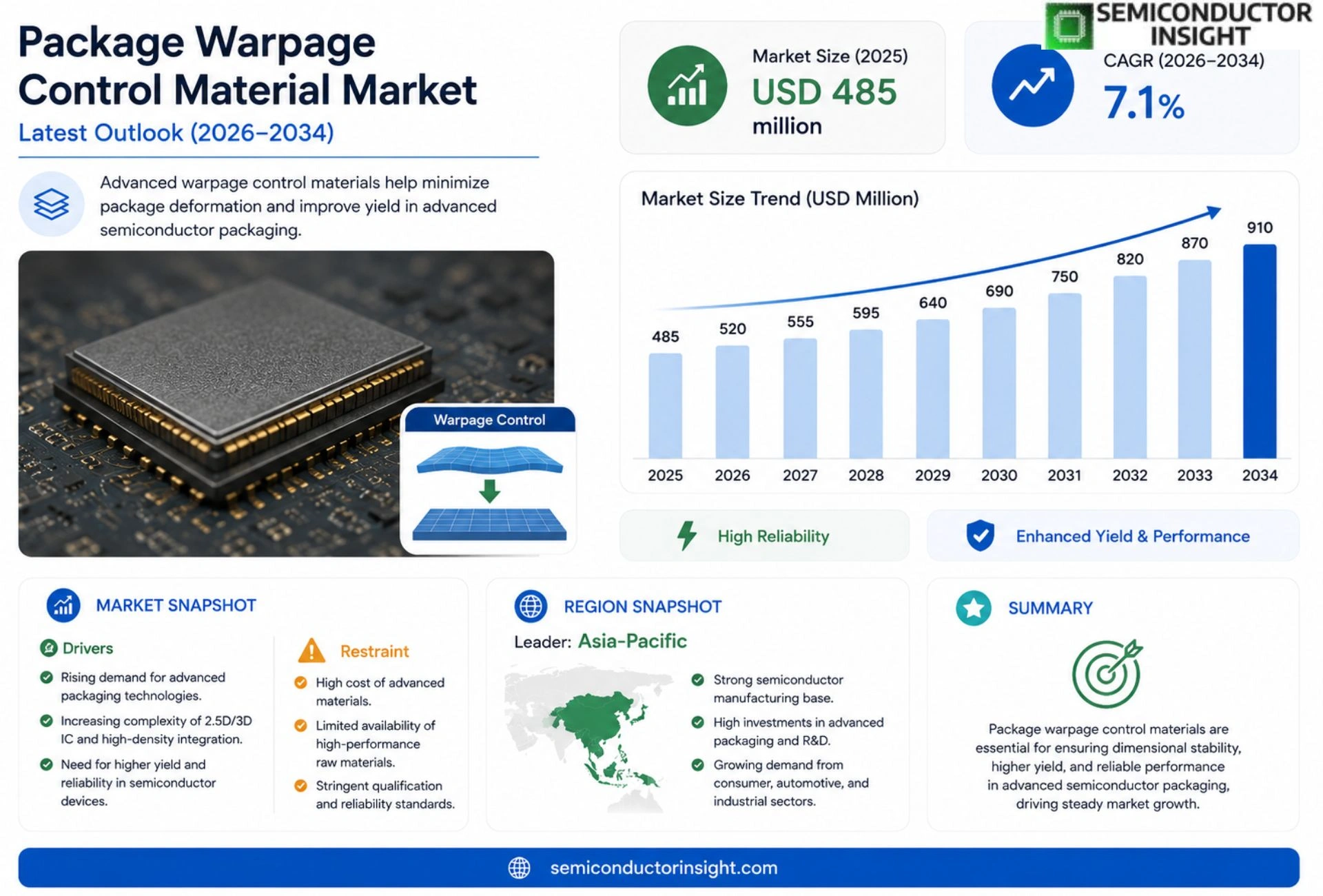
Global Package Warpage Control Material Market size was valued at USD 485 million in 2025. The market is projected to grow from USD 520 million in 2026 to USD 910 million by 2034, exhibiting a CAGR of 7.1% during the forecast period.
Package warpage control materials are specialized compounds engineered to mitigate thermal and mechanical stresses during semiconductor packaging processes. These materials,primarily comprising epoxy molding compounds (EMCs), underfill resins, die attach adhesives, and thermal interface materials (TIMs),are designed to counteract warpage induced by coefficient of thermal expansion (CTE) mismatches between silicon dies, substrates, and encapsulants. Their formulation often integrates fillers such as silica or alumina to enhance dimensional stability while maintaining electrical insulation and heat dissipation properties. Because advanced packaging technologies like fan-out wafer-level packaging (FOWLP), system-in-package (SiP), and 3D IC integration demand ultra-thin profiles and high-density interconnects, the role of these materials has become critical in ensuring yield reliability across consumer electronics, automotive chips, and high-performance computing applications.
The market is expanding due to the relentless miniaturization of electronic devices and the transition toward heterogeneous integration architectures. While traditional epoxy-based solutions dominate current adoption, innovations in low-stress formulations,particularly those leveraging nanoparticle reinforcement,are gaining traction as manufacturers seek to address warpage challenges in next-generation packages exceeding 10 mm × 10 mm dimensions. Furthermore, regulatory pressures for halogen-free compositions are reshaping material chemistries without compromising performance benchmarks.
MARKET DRIVERS
Rapid Advancements in Semiconductor Packaging
The global Package Warpage Control Material Market is experiencing substantial traction, primarily driven by the relentless miniaturization of electronic components. As semiconductor fabrication nodes shrink, the thickness differential between silicon dies and organic substrates increases, creating significant mechanical stress. This necessitates the deployment of specialized control materials to manage thermal expansion coefficients and ensure structural integrity. Manufacturers are increasingly adopting these materials to boost yield rates in high-volume production environments, directly fueling market demand.
Surge in Portable Electronics and Wearables
The boom in consumer electronics, particularly in smartphones, tablets, and smartwatches, has created a parallel demand for thinner, lighter, and more robust components. The transition to flexible printed circuit boards (FPCBs) and ceramic packages has exacerbated warpage issues, necessitating advanced interposers and bonding materials. Analysts project that the integration of warpage control solutions will be a key differentiator for major OEMs aiming to deliver high-performance, portable devices without compromising reliability.
➤ Precise dimensional control is critical for the successful deployment of next-generation 5G infrastructure modules.
Furthermore, the industrialization of the Internet of Things (IoT) ecosystem requires components that can withstand harsh environmental conditions. High-reliability electronics, such as automotive controllers and industrial sensors, rely on warpage mitigation materials to prevent failure during operation.
MARKET CHALLENGES
High Manufacturing Costs of Advanced Materials
The implementation of high-performance warpage control solutions often entails significant initial investment. Advanced thermosetting resins and specialized molding compounds are costly to produce, which is reflected in the end price of semiconductor packaging equipment. This price sensitivity can be a barrier for small and medium-sized enterprises (SMEs) operating on thin margins, potentially slowing down the widespread adoption of sophisticated control strategies in less capital-intensive sectors.
Other Challenges
Technical Expertise Gap
Effective warpage management is a complex engineering process that requires a deep understanding of thermal dynamics and material science. A shortage of skilled personnel proficient in these niche technologies poses a challenge to manufacturers attempting to integrate advanced control materials efficiently.
Compatibility Issues
Integrating new control materials into existing assembly workflows without disrupting production schedules is often difficult. The need for specialized testing equipment and calibration procedures adds to the operational complexity for manufacturers.
MARKET RESTRAINTS
Volatile Raw Material Prices
The aggregate cost of raw materials, including specialty resins, fillers, and adhesives, is subject to significant market fluctuations. Price volatility in the chemical commodities market can directly impact the operational costs of packaging material suppliers. Consequently, maintaining stable pricing structures for end-users becomes difficult, which may deter long-term contracts and strategic investment in new packaging technologies that utilize these materials.
Stringent Regulatory Environments
Global regulations regarding chemical safety and environmental impact, such as RoHS and REACH, necessitate strict monitoring of material compositions. Developing new warpage control materials that are compliant with these regulations requires extensive research and testing, increasing the time-to-market for innovative products and imposing a compliance cost burden on manufacturers.
MARKET OPPORTUNITIES
Expansion in Automotive Electronics and EVs
The rapid electrification of the automotive sector presents a massive opportunity for Package Warpage Control Material Market. Electric vehicle (EV) powertrain electronics, including battery management systems (BMS) and onboard chargers, operate under extreme thermal cycles. The demand for robust, high-reliability packaging materials capable of withstanding these conditions is projected to grow exponentially, offering lucrative prospects for material suppliers and semiconductor package providers.
Adoption of Advanced Packaging Techniques
The industry is shifting towards Advanced Packaging (AP) solutions such as fan-out wafer-level packaging (FoP) and Chip Stacked Packages (CSP). These techniques involve complex stacking and interconnections that are highly susceptible to warpage. The move towards 2.5D and 3D packaging architectures creates a critical need for materials that can manage stress across multiple layers, driving the demand for specialized control materials.
Collaborations between material science firms and semiconductor manufacturers to develop custom-tailored solutions will likely define the growth trajectory of this market in the coming decade.
Trends
Scaling of 2.5D and 3D Integration Technologies
The global Package Warpage Control Material Market is experiencing robust expansion driven by the rapid adoption of heterogeneous integration architectures and the widespread scaling of 2.5D and 3D IC technologies. As the semiconductor industry shifts toward high-density interconnects in advanced packaging, the demand for specialized compounds engineered to mitigate thermal and mechanical stresses has surged to new heights. Current market analysis indicates a valuation reached USD 485 million in 2025, with projections escalating to USD 910 million by 2034, supported by a steady CAGR of 7.1% during the forecast period. This sustained growth is closely correlated with the rising complexity of production lines and the critical necessity for yield reliability in advanced packaging environments where thermal cycles can induce significant mechanical stress on delicate interconnections.
Other Trends
Material Composition and CTE Mismatch Management
Market expansion is largely fueled by the relentless miniaturization of electronic devices and the transition to system-in-package (SiP) and fan-out wafer-level packaging (FOWLP) solutions. Because advanced packaging demands ultra-thin profiles, the role of materials in counteracting warpage induced by coefficient of thermal expansion (CTE) mismatches between silicon dies and organic substrates is critical for operational longevity. Specialized compounds, often integrating silica or alumina fillers to enhance dimensional stability, are now essential to balance performance properties while maintaining strict electrical insulation and efficient heat dissipation standards required for consumer electronics.
Innovative Low-Stress Formulations
While traditional epoxy-based molding compounds dominate current adoption, the market is undergoing a significant evolution driven by the need for next-generation performance in high-performance computing and automotive sectors. Innovations in low-stress formulations are gaining traction as manufacturers tackle warpage challenges in packages exceeding 10 mm × 10 mm dimensions. Furthermore, a distinct trend involves navigating regulatory pressures for halogen-free compositions, which necessitates active chemical restructuring. Formulations are actively being redesigned to meet stringent environmental safety standards while preserving necessary performance benchmarks that ensure long-term reliability in complex hardware systems.
COMPETITIVE LANDSCAPE
Key Industry Players
Global market valued at USD 485 million in 2025 with CAGR of 7.1%
The global package warpage control material market is experiencing significant expansion, valued at USD 485 million in 2025 and projected to reach USD 910 million by 2034. The competitive landscape is defined by leading material suppliers utilizing epoxy molding compounds and thermal interface materials to mitigate CTE mismatches. These companies focus on developing specialized compounds designed for advanced packaging technologies like fan-out wafer-level packaging (FOWLP) and 3D IC integration.
As the industry shifts towards heterogeneous integration and regulatory pressures enforce halogen-free compositions, significant competition exists regarding material performance and dimensional stability. Key players are increasingly investing in nanoparticle reinforcement technologies to maintain electrical insulation while solving warpage challenges in next-generation packages exceeding 10 mm × 10 mm dimensions, thereby driving innovation in yield reliability for consumer electronics and automotive applications.
List of Key Package Warpage Control Material Companies Profiled
- Dow
- Dow
- Huntsman
- 3M
- Momentive
- Kyocera
- Kyocera
- Sumitomo Bakelite
- Shin-Etsu
- Hitachi Chemical
- Sumitomo Chemical
- Nanocs
- Fujipoly
- LG Chem
- LG Chem
Segment Analysis:
| Segment Category | Sub-Segments | Key Insights |
| By Type |
|
Epoxy Molding Compounds are currently the leading technology in the market due to their widespread use in semiconductor encapsulation, offering critical protection against moisture and mechanical shock while effectively managing thermal expansion mismatches. Underfill Resins are increasingly utilized in advanced packaging processes to reinforce interconnects and reduce shear stress during thermal cycling, thereby enhancing overall mechanical reliability. Die Attach Adhesives serve as a vital thermal interface material, selected for their high thermal conductivity and bonding strength to ensure efficient heat dissipation between silicon dies and the substrate. |
| By Application |
|
Fan-out Wafer Level Packaging requires materials that offer high flexibility to accommodate complex interconnections across multiple dies. System-in-Package (SiP) architectures demand robust material formulations that can support heterogeneous integration without inducing detrimental warpage during thermal operations. 3D IC Integration necessitates ultra-thin profiles and high-density interconnects, putting a premium on materials that maintain mechanical integrity and dimensional stability at the nanoscale. |
| By End User |
|
Consumer Electronics drive demand through relentless miniaturization trends that require materials capable of managing tight thermal budgets in slim devices. The Automotive Sector imposes stringent reliability standards due to operation under harsh temperature extremes, making material specificity critical for long-term durability. High-Performance Computing applications demand materials with superior thermal management capabilities to sustain high heat loads without compromising dimensional accuracy or yield rates. |
| By Fillers |
|
Silica Based Fillers are the standard choice for enhancing dimensional stability and reducing CTE, though they often increase viscosity. Alumina Based Fillers are favored for their superior electrical insulation and thermal conductivity properties, particularly in high-power applications. Hollow Glass Microspheres represent an innovative alternative used to reduce package weight and lower CTE without adding significant density, addressing the trade-off between stiffness and weight in advanced packaging solutions. |
| By Formulation |
|
Low-Stress Epoxy Formulations have become essential for larger die sizes to minimize internal stress that can lead to cracking or delamination. Nanoparticle Reinforced Materials offer cutting-edge solutions by allowing precise tailoring of material properties at the molecular level, effectively optimizing performance for next-generation packaging needs. Halogen-Free Composites are gaining significant traction to meet evolving environmental and regulatory standards regarding chemical composition without sacrificing the high thermal protection required for reliable operation. |
Regional Analysis: Package Warpage Control Material Market
High-performance polymer materials are gaining significant traction as they provide exceptional dimensional accuracy and thermal resistance, essential for minimizing warpage in complex semiconductor packaging structures.
Metal laminates offer robust mechanical support and shielding properties, effectively counteracting thermal expansion differences that cause deformation in electronic assemblies during critical processing cycles.
Advanced adhesive formulations play a crucial role by bonding materials with different thermal coefficients, thereby reducing internal stress and preventing package warpage at the critical bonding interface.
Precision sizing solutions are utilized to optimize the fit of internal components, ensuring that expansion and contraction do not lead to mechanical misalignment or physical warping of the device shell.
Europe
Europe commands a substantial market share for package warpage control material due to its stronghold in the automotive and industrial machinery sectors, where reliability is paramount. The region is driven by strict regulatory standards that mandate high durability and energy efficiency for electronic components. Manufacturers in Germany and France are increasingly investing in domestic warpage control solutions to reduce supply chain dependencies and ensure strict compliance with environmental and safety norms. The focus here is on sustainable material choices without compromising the efficacy of controlling deformation, leading to a unique market evolution in the package warpage control material sector.
Asia-Pacific
The Asia-Pacific region represents the largest volume hub for package warpage control material consumption, fueled by the rapid expansion of consumer electronics and semiconductor fabrication capabilities. Countries like South Korea, Taiwan, and China have established massive supply chains that require cost-effective yet efficient controlling materials. The intense competition in the local market ensures continuous innovation in material application techniques to handle high throughput manufacturing demands. While cost sensitivity is high, the scale of production in this region necessitates bulk processing optimization, driving the adoption of standardized and highly effective warpage prevention strategies tailored to high-volume production lines.
South America
South America is witnessing a gradual increase in demand for package warpage control material, primarily driven by the maturing electronics assembly industry and growing infrastructure projects. Markets in Brazil and Chile are focusing on improving the quality of domestically produced electronic components as they look to enter higher value-added supply chains. The emphasis remains on affordable materials that can withstand diverse climatic conditions while maintaining the structural integrity of electronic packages during storage and transport. As the region modernizes its technological capabilities, the adoption of specialized control materials is expected to accelerate to support broader modernization efforts.
Middle East & Africa
The Middle East and Africa region is an emerging market for package warpage control material, characterized by a transition from basic component assembly to more sophisticated assembly processes. With increasing investments in smart city initiatives and renewable energy projects, there is a rising need for reliable electronic control units. Local distributors are bridging the gap by bringing in specialized materials suited for harsh environments. The market growth is steady and is largely dependent on foreign direct investment in manufacturing technology, which inherently includes the requirement for high-quality materials to effectively manage thermal stress and warpage in diverse operational settings.
Report Scope
This market research report provides a comprehensive analysis of the Package Warpage Control Material Market , covering the forecast period 2026–2034. It offers detailed insights into market dynamics, technological advancements, competitive landscape, and key trends shaping the industry.
Key focus areas of the report include:
- Market Overview: The report begins with an overview outlining its current market scenario, key growth indicators, and industry transformation drivers. It discusses macroeconomic factors, demand–supply balance, regulatory landscape, and the strategic role of semiconductors in powering advancements across industries such as automotive, telecommunications, consumer electronics, and industrial automation.
- Market Size & Forecast: Historical data and future projections for revenue, unit shipments, and market value across major regions and segments.
- Segmentation Analysis: Detailed breakdown by product type, technology, application, and end-user industry to identify high-growth segments and investment opportunities.
- Regional Insights: Insights into market performance across North America, Europe, Asia-Pacific, Latin America, and the Middle East & Africa, including country-level analysis where relevant.
- Competitive Landscape: Profiles of leading market participants, including their product offerings, R&D focus, manufacturing capacity, pricing strategies, and recent developments such as mergers, acquisitions, and partnerships.
- Technology Trends & Innovation: Assessment of emerging technologies, integration of AI/IoT, semiconductor design trends, fabrication techniques, and evolving industry standards.
- Market Drivers & Restraints: Evaluation of factors driving market growth along with challenges, supply chain constraints, regulatory issues, and market-entry barriers.
- Stakeholder Insights: Insights for component suppliers, OEMs, system integrators, investors, and policymakers regarding the evolving ecosystem and strategic opportunities.
Primary and secondary research methods are employed, including interviews with industry experts, data from verified sources, and real-time market intelligence to ensure the accuracy and reliability of the insights presented.
FREQUENTLY ASKED QUESTIONS:
What is the current market size of Package Warpage Control Material Market?
-> Package Warpage Control Material Market size was valued at USD 485 million in 2025. The market is projected to grow from USD 520 million in 2026 to USD 910 million by 2034, exhibiting a CAGR of 7.1% during the forecast period.
Which key companies operate Package Warpage Control Material Market?
-> Key players include Axalta Coating Systems, AkzoNobel, BASF SE, PPG, Sherwin-Williams, and 3M, among others.
What are the key growth drivers?
-> Key growth drivers include relentless miniaturization of electronic devices and transition toward heterogeneous integration architectures.
Which region dominates the market?
-> Asia-Pacific is the fastest-growing region, while Europe remains a dominant market.
What are the emerging trends?
-> Emerging trends include innovations in low-stress formulations, nanoparticle reinforcement, and halogen-free compositions.

Get Sample Report PDF for Exclusive Insights
Report Sample Includes
- Table of Contents
- List of Tables & Figures
- Charts, Research Methodology, and more...
 Download Sample Report PDF

