Key Statistics
Key Takeaways
- Laser & detector chips remain the central type because every pluggable or co-packaged optical path needs an optical source and receiver; the mix is shifting toward 200G-per-lane EMLs, VCSELs and higher-power continuous-wave lasers as 1.6T links enter deployment.
- 800G optical modules are the highest-bandwidth application explicitly listed on the source page, but the technology roadmap is already moving beyond that boundary: Coherent, Lumentum, MACOM and Semtech all demonstrated or sampled 1.6T-class building blocks during 2025–2026.
- Asia Pacific is the largest region in the source page, supported by dense optical-component manufacturing, telecom equipment production and hyperscale infrastructure in China, Japan, South Korea and the broader Asian supply chain.
- AI changes the chip mix rather than simply increasing unit volume. 200G-per-lane drivers, TIAs, EMLs, VCSELs, photodiodes, CW lasers and silicon-photonics interfaces command more engineering content because power, thermal and signal-integrity constraints tighten with every speed generation.
- Interoperability is becoming a commercial gate. OIF demonstrations in 2025 included CEI-224G, CEI-448G, 800ZR, co-packaging and energy-efficient interfaces, showing that suppliers must design chips around multi-vendor electrical, optical and management ecosystems rather than proprietary links alone.
Optical Module Chip Market Overview
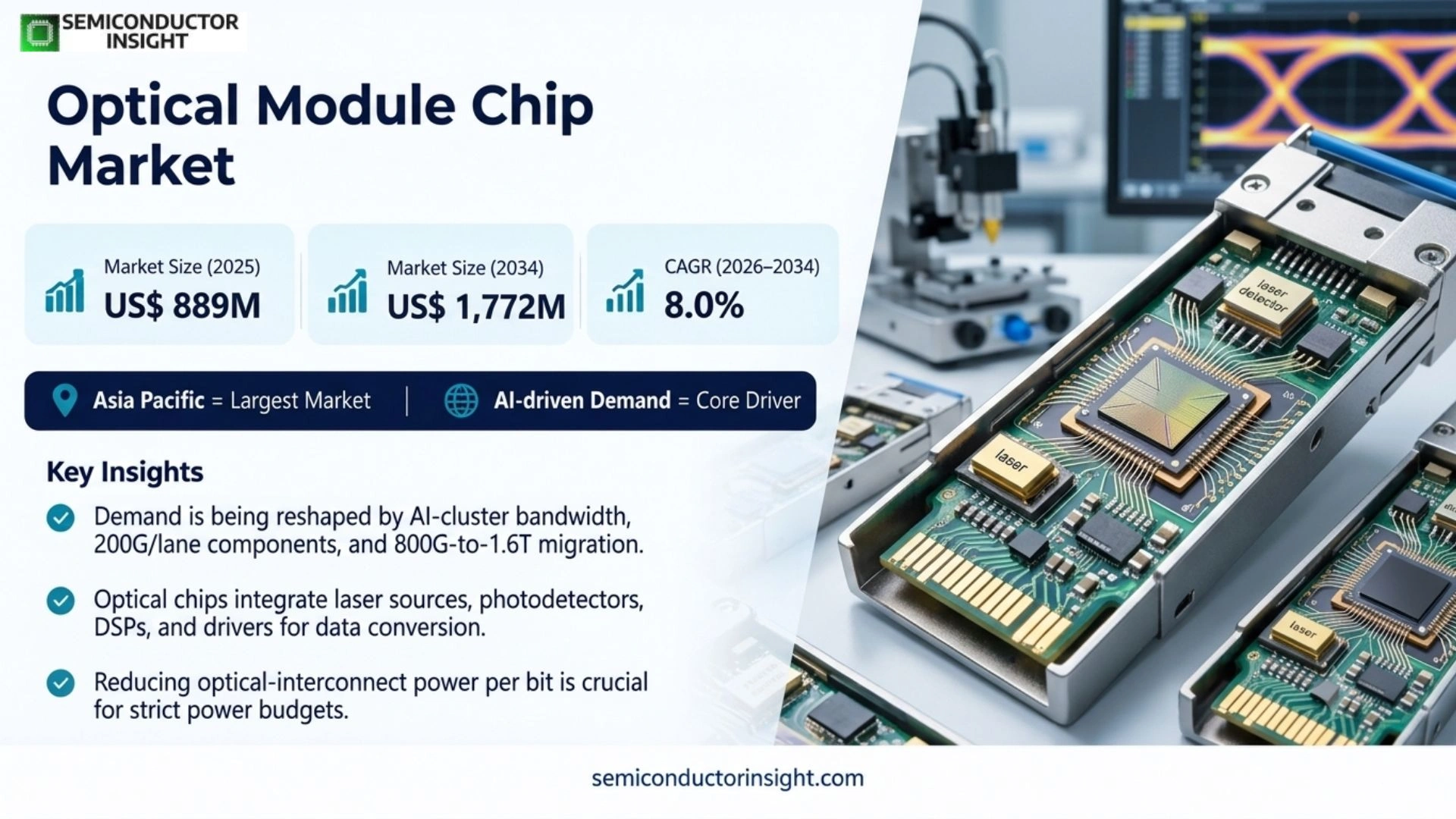
Optical module chip market is rebased to USD 889 million in 2025, increases to an estimated USD 959 million in 2026, and is projected to reach USD 1.77 billion by 2034. The two source-page size anchors imply a 8.0% CAGR during 2026–2034. Asia Pacific is the largest market in 2025, while current demand is being reshaped by AI-cluster bandwidth, 200G-per-lane component ramps, 800G-to-1.6T migration, silicon photonics and the need to reduce optical-interconnect power per bit.
Optical module chips are the semiconductor building blocks inside optical transceivers and related photonic engines. The category spans laser sources, photodetectors, driver and transimpedance-amplifier ICs, optical DSP and transceiver-control ICs, multiplexing functions and silicon-photonics devices. Their commercial value comes from converting high-speed electrical data into optical signals, carrying those signals through fiber with acceptable loss and noise, and then recovering the data within a strict module-level power and thermal budget.
Bandwidth scaling is forcing the component stack to evolve in parallel. IEEE’s 1.6 Tb/s Ethernet work is based on 200 Gb/s or greater per-lane signaling, while OIF interoperability programs now cover CEI-224G and CEI-448G electrical interfaces alongside 800ZR and co-packaging. That roadmap matters directly to chip suppliers because every increase in lane rate changes laser modulation bandwidth, detector response, TIA noise, driver swing, package parasitics and the DSP complexity needed to close the link.
Recent product activity confirms that the market is moving from laboratory feasibility into production-oriented component design. Coherent demonstrated 1.6T transceivers based on 200G VCSELs in April 2025; MACOM launched four 200G-per-lane solutions for 1.6T data-center connectivity in March 2025; Semtech began sampling 200G/channel VCSEL-driver and TIA building blocks in September 2025; and Lumentum stated in 2026 that 1.6T and 200G-per-lane technologies were moving into deployment. The implication is a broader, higher-value semiconductor bill of materials for each optical port.
Segment Analysis: By Type
The source page segments the market into Laser & Detector Chip; Amplifiers, Drivers and MUX/DEMUX Chip; Optical Transceiver ICs; Silicon Photonics Chips; and Others. Laser and detector devices form the optical conversion layer, while drivers, TIAs, DSP/control functions and silicon photonics determine how efficiently those optical devices can be operated at 100G, 200G and future 400G-per-lane speeds.
| Type | Technical / commercial role | Market position |
|---|---|---|
| Laser & Detector Chip | This category includes VCSELs, DFB lasers, EMLs, photodiodes and related optical-source or receiver dies. Performance requirements rise with lane speed because extinction ratio, chirp, responsivity, bandwidth, thermal behavior and coupling efficiency determine whether the module can meet reach and error-rate targets. InP is critical for many single-mode laser products, while GaAs VCSELs remain important for short-reach multimode data-center links. | Largest strategic device class. Coherent demonstrated 200G VCSEL-based 1.6T optics, while Lumentum’s 200G EML product is designed for 1.6T modules with eight 200G lanes. The segment benefits directly from AI scale-out networks because the optical source and detector cannot be eliminated even as packaging architectures move from pluggables toward near- or co-packaged optics. |
| Amplifiers, Drivers and MUX/DEMUX Chip | Driver ICs translate electrical SerDes outputs into the voltage or current swing required by EMLs, VCSELs or modulators, while TIAs recover very small detector currents at the receive side. Multiplexing devices combine or separate wavelengths. At 200G per lane, package parasitics and power become first-order constraints, so these chips increasingly use advanced analog processes and tightly controlled co-design with the optical device. | Fast-rising enabling segment. MACOM’s 2025 portfolio added 200G-per-lane components for 1.6T, and Semtech’s 2025 FiberEdge sampling combined a 200G VCSEL driver with a 200G-channel TIA. These launches show that hyperscale demand pulls an entire analog front-end ecosystem, not only lasers, and that vendors able to qualify paired transmit and receive solutions can capture more module content. |
| Optical Transceiver ICs | Transceiver ICs include DSPs, clocking, control and monitoring functions that condition PAM4 data, manage equalization, support forward error correction interfaces and coordinate module behavior through standards such as CMIS. As link speeds increase, these chips are pushed toward smaller process nodes to reduce power, while firmware sophistication becomes an important differentiator for multi-vendor interoperability and field diagnostics. | High-value control and signal-processing layer. Coherent’s 2025 silicon-photonics 1.6T demonstration used a 3 nm optical DSP and highlighted more than 20% targeted power reduction versus prior-generation DSP technology. The commercial opportunity is therefore tied to both speed and watts per bit, with module vendors willing to adopt newer silicon when it materially eases thermal and front-panel density constraints. |
| Silicon Photonics Chips | Silicon photonics integrates waveguides, modulators, couplers and wavelength functions on a silicon-compatible manufacturing platform. It can raise integration density and support wafer-scale processes, but still depends on external or heterogeneously integrated laser sources because silicon is inefficient as a light emitter. The architecture is central to many 800G, 1.6T and co-packaged designs where electrical reach and fiber density become limiting system constraints. | Strategic integration platform rather than a complete substitute for III-V chips. Coherent’s 1.6T DR8 demo combined silicon photonics with an advanced DSP, while Lumentum supplies high-power lasers intended to feed silicon-photonics engines. The segment therefore expands the addressable market for both silicon photonics and external laser chips, creating complementary rather than purely substitutive component demand. |
| Others | The residual category includes specialty monitoring photodiodes, wavelength-control devices, optical switching or interface chips, and application-specific photonic components not captured in the major classes. These products often have lower unit volumes but can carry high qualification value because they solve thermal monitoring, power control, coherent-networking or specialty-reach requirements inside complex optical subsystems. | Niche but technically defensible. As optical architectures diversify across pluggable, near-packaged, co-packaged, coherent and short-reach multimode designs, module makers need additional control and monitoring functions. Suppliers can defend attractive positions when a specialty device reduces calibration time, improves reliability or enables a specific link budget that cannot be met by a standardized high-volume chip. |
Secondary segmentation: By Transmission Distance
The source page additionally divides the market into Short-reach (up to 10 km), Medium-reach (10–40 km), and Long-haul (above 40 km). Reach changes the semiconductor content because short links prioritize low power and cost, while longer links require stronger laser performance, wavelength stability, amplification, coherent processing or higher link-margin engineering.
| Transmission distance | Chip implications |
|---|---|
| Short-reach — up to 10 km | AI clusters and data centers dominate this reach class, where 100G- and 200G-per-lane PAM4 links need extreme bandwidth density at low watts per bit. VCSELs can serve very short multimode links, while EML and silicon-photonics solutions address single-mode reaches. The purchasing trigger is often total switch-rack power and port density rather than absolute fiber reach. |
| Medium-reach — 10–40 km | Metro access, 5G transport and campus or inter-building links require better optical budgets and wavelength control than intra-data-center connections. Chip suppliers must balance transmitter power, receiver sensitivity and thermal behavior with module cost. WDM functions become more important because operators want to increase capacity without multiplying fiber count across existing transport routes. |
| Long-haul — above 40 km | Long-haul links increasingly rely on coherent optics, optical DSP, high-performance modulators, tunable lasers and amplification. The semiconductor bill of materials is more complex and expensive, but unit volumes are lower than short-reach datacom. Supplier differentiation depends on optical linewidth, DSP performance, photonic integration, reliability and interoperability with carrier-grade transmission platforms. |
Segment Analysis: By Application
By application, the source page segments demand into 10/25G, 100G, 200G, 400G and 800G optical modules. The commercial center is migrating rapidly toward 400G and 800G in cloud networks, while 1.6T products—outside the source page’s stated application list but already demonstrated commercially—are creating the next component-design cycle around 200G-per-lane optics.
| Application | Demand characteristics |
|---|---|
| 10/25G Optical Module | These lower-speed modules remain widely used in access, enterprise and 5G fronthaul applications because cost and installed compatibility matter more than maximum bandwidth. Chip suppliers compete on mature manufacturing, low power and price, but the segment faces persistent ASP pressure as production shifts toward standardized architectures and high-volume Asian manufacturing. |
| 100G Optical Module | 100G remains an important enterprise, telecom and installed data-center speed, using combinations of 25G or 50G lanes depending on architecture. Demand is supported by upgrades from 10G/40G networks, but the growth premium has moved to faster links. Component vendors therefore optimize mature 100G products for cost while reusing process platforms to fund newer 200G-per-lane development. |
| 200G Optical Module | 200G serves data-center aggregation, telecom and transitional architectures where 400G is not yet required or economical. The segment is technically important because it familiarized the ecosystem with higher-order PAM4 signaling and tighter signal-integrity requirements, providing a manufacturing bridge toward 400G and 800G products. |
| 400G Optical Module | 400G became a major cloud and data-center interconnect speed and remains a high-volume platform for DR4, FR4 and coherent applications. The modules pull 100G-per-lane EMLs, silicon photonics, photodiodes, drivers, TIAs and DSPs. The commercial challenge is aggressive cost-per-bit reduction as hyperscalers move new network builds toward 800G. |
| 800G Optical Module | 800G is the highest-speed application explicitly listed on the source page and is central to current AI scale-out fabrics. Designs use eight 100G lanes or increasingly four 200G optical lanes depending on implementation. The move to 200G-per-lane components is especially important because it reduces lane count, module complexity and I/O density while establishing the technology base for 1.6T. |
Secondary segmentation: By End User
The source page also segments end users into Telecom Service Providers, Data Centers, Enterprise Networks and Others. Each buyer group evaluates optical chips indirectly through module specifications, but their priorities differ: hyperscalers optimize watts per bit and density, carriers emphasize reach and interoperability, and enterprise buyers value standardized cost-effective modules.
| End user | Purchasing logic |
|---|---|
| Telecom Service Providers | Carrier networks use optical modules in access, metro, backhaul and long-haul infrastructure. Component selection is mediated through system and module vendors, with reliability, wavelength control, reach, temperature range and standards compliance taking priority. 5G transport adds volume at 25G, 100G and higher rates, while coherent pluggables pull sophisticated DSP and laser content. |
| Data Centers | Data centers are the fastest technology-transition engine because AI training and inference require massive east-west traffic among accelerators. Coherent, Lumentum, MACOM and Semtech are all developing 200G-per-lane building blocks for 1.6T architectures, showing that hyperscale buyers increasingly shape laser, detector, driver, TIA and photonics roadmaps through power and density targets. |
| Enterprise Networks | Enterprise demand is more conservative, with longer deployment cycles and a stronger focus on interoperability, availability and acquisition cost. This sustains 10G, 25G, 100G and selected 400G modules after hyperscalers have moved to faster generations. Chip suppliers can therefore monetize mature processes longer, although pricing declines faster once products become broadly standardized. |
| Others | Other users include research, government, industrial and specialty communication systems. Their volumes are smaller but technical requirements can be unusual, including wide temperature, radiation tolerance, custom wavelengths or extended lifecycle support. These requirements can create profitable niches for component suppliers able to maintain specialized processes after mainstream data-center products migrate to newer speeds. |
Regional Analysis
The source page identifies Asia Pacific as the largest market, led by China, Japan and South Korea. North America is the primary technology-demand center for AI hyperscale networks and many leading photonics suppliers, Europe contributes telecom and industrial photonics demand, while South America and the Middle East & Africa remain more import-dependent and infrastructure-led.
Why does the optical module chip market behave differently by region?
Regional economics split between where optical components are designed, where they are manufactured and where the highest-value network systems are deployed. North America influences the roadmap through hyperscale AI and merchant silicon. Asia Pacific combines optical-module assembly, telecom equipment and semiconductor manufacturing. Europe has deep photonics research and carrier infrastructure. Emerging regions mainly buy finished modules, so chip demand appears indirectly through imported network equipment rather than local semiconductor production.
| Region | Position | Growth outlook | Demand profile | What decides supplier selection |
|---|---|---|---|---|
| Asia Pacific | Largest | High | Manufacturing, telecom and data-center led | Cost, scale, local supply, qualification and multi-speed portfolio |
| North America | Technology-demand leader | High | AI hyperscale and cloud-led | Power per bit, 1.6T readiness, reliability and integration |
| Europe | Established | Moderate to high | Carrier, industrial and photonics-led | Standards, energy efficiency, coherent reach and quality |
| South America | Smaller | Moderate | Telecom modernization-led | Landed cost, availability and proven module interoperability |
| Middle East & Africa | Emerging | Moderate from small base | Data-center, subsea and telecom-led | Supply reliability, temperature range and system support |
Competitive Landscape
Competition spans vertically integrated photonics companies, analog and mixed-signal semiconductor suppliers, module specialists and regional Chinese manufacturers. Coherent and Lumentum are strong in lasers, detectors and photonic integration; MACOM and Semtech compete in drivers, TIAs and optical semiconductor building blocks; Accelink, Hisense, Source Photonics and other module-oriented players integrate chips into broader optical products.
The competitive advantage increasingly comes from co-design across optical and electrical layers. A 200G EML cannot be evaluated independently of the driver, package, fiber coupling and receiver path because each contributes to link margin and power. Suppliers with internally matched transmitter and receiver building blocks can shorten module-development cycles, while specialist chip vendors remain competitive when they deliver superior analog performance and reference designs that integrate cleanly with third-party optics.
Manufacturing scale has become as important as laboratory performance. Lumentum disclosed in 2026 that it was expanding EML capacity and building additional U.S. InP manufacturing, while its strategic agreement with NVIDIA included capacity access rights. This signals that hyperscalers increasingly treat optical semiconductors as strategic capacity because AI network growth can consume millions of high-speed optical lanes and expose the system to supply shortages if laser or detector output is constrained.
Chinese suppliers compete strongly on module cost and local telecom relationships, creating price pressure for mature 25G, 100G and 400G components. Western and Japanese suppliers defend positions through high-performance InP, VCSEL, detector and analog technology, while silicon-photonics platforms change the value chain by moving more passive and modulator functionality onto integrated photonic circuits. The market is therefore fragmented by function even when a few firms lead specific device categories.
| Competitive tier | Companies | Why they matter |
|---|---|---|
| Integrated photonics leaders | Coherent Corp; Lumentum; HAMAMATSU | These suppliers combine optical-device know-how, high-volume manufacturing and strong reliability records. Coherent and Lumentum are directly demonstrating 1.6T and 200G-per-lane technologies, while Hamamatsu brings deep detector expertise. Their advantage is the ability to qualify advanced optical devices at scale rather than relying solely on merchant analog or control ICs. |
| High-speed semiconductor specialists | MACOM; SEMTECH; Maxim Integrated | This tier competes in laser drivers, TIAs, analog interfaces, DSP or related semiconductor functions that determine whether high-speed optical devices can operate efficiently. MACOM and Semtech launched 200G-per-lane products for 1.6T in 2025, illustrating how analog bandwidth, power and package co-design are now central competitive parameters. |
| Module and regional ecosystem players | Accelink Technologies; Hisense; Shenzhen Sijie Smart Sensing Technology; Broadex Technologies; HGTECH; Source Photonics; Wuhan Minsemicondutor; Hisilicon | These companies participate through module integration, local manufacturing, component design or regional customer relationships. Their commercial leverage is strongest in Asia-Pacific telecom and data-center supply chains, where rapid qualification, cost control and access to local module assembly can offset smaller global semiconductor portfolios. |
Companies profiled in the report
The source page profiles Coherent Corp, Lumentum, Maxim Integrated, HAMAMATSU, Accelink Technologies, Hisense, Shenzhen Sijie Smart Sensing Technology, Broadex Technologies, HGTECH, MACOM, SEMTECH, Source Photonics, Wuhan Minsemicondutor and Hisilicon. The article preserves that company scope while distinguishing optical-device leaders, high-speed semiconductor specialists and module-oriented or regional participants. The result is a market in which engineering credibility and dependable execution create measurable commercial value, particularly when customers are qualifying products for long-lived infrastructure or semiconductor platforms.
Production Capacity Analysis
Production capacity is constrained by a mix of III-V wafer fabrication, epitaxial growth, high-speed analog semiconductor processes, photonic wafer processing, packaging and automated optical test. A nominal chip fab cannot immediately become an optical-chip source because laser and detector performance depends on specialized material systems, while final yield depends heavily on precision coupling, wafer screening and module-level electro-optical characterization.
InP and GaAs device manufacturing are particularly important for lasers, VCSELs and detectors. Lumentum’s 2026 U.S. manufacturing announcement targeted a 240,000-square-foot facility for InP-based products, while the NVIDIA agreement included future capacity access for advanced laser components. These actions show that laser wafer capacity can become a strategic bottleneck when 800G and 1.6T deployments accelerate faster than existing epitaxy and fab output can scale.
High-speed analog capacity must rise in parallel. Drivers and TIAs at 200G per lane operate at bandwidths where package parasitics, substrate loss and process variation materially affect yield. Semtech’s 200G/channel PMD devices and MACOM’s 1.6T component portfolio illustrate the need for coordinated device, package and test capability rather than commodity analog manufacturing. Suppliers that control characterization and reference designs can reduce customers’ integration risk.
Silicon photonics changes the capacity equation by allowing some optical functions to use silicon-compatible wafer processes, but it does not eliminate the III-V supply chain. Many silicon-photonics architectures still require CW or ultra-high-power lasers made from InP or other direct-bandgap materials. As a result, the fastest-growing production model is heterogeneous: silicon photonics provides integration density while specialized external lasers and high-speed electronics remain separate but tightly co-designed capacity pools.
Market Dynamics
The market is pulled by AI bandwidth and 200G-per-lane technology while restrained by optical-device capacity, rapid ASP erosion and the engineering difficulty of moving from demonstration to reliable high-volume production. The decisive commercial metric is shifting from dollars per module toward bandwidth delivered per watt, per fiber and per front-panel area.
Market Drivers
| Driver | Directional impact* | Commercial mechanism |
|---|---|---|
| AI and hyperscale networking | High | AI clusters require far more east-west bandwidth than traditional enterprise networks. The transition to 800G and 1.6T increases laser, detector, driver, TIA and photonic content per switch generation, while hyperscaler qualification gives successful components access to very large volumes. |
| 200G-per-lane transition | High | IEEE and OIF roadmaps are standardizing 200G-class electrical and optical interfaces. Fewer lanes can deliver the same aggregate throughput, improving density but requiring materially faster devices. This creates a new replacement cycle for analog front ends, EMLs, VCSELs, photodiodes and DSPs. |
| Power and thermal constraints | Medium to High | Data centers cannot scale networking power linearly with bandwidth. Smaller-node DSPs, lower-drive-voltage lasers, silicon photonics and co-packaging all aim to reduce watts per bit. Components that cut power can command design wins even when their purchase price is higher. |
| 5G and carrier upgrades | Medium | Telecom networks continue to require 25G, 100G, 400G and coherent optics for fronthaul, backhaul and metro capacity. This provides a broad demand base outside AI data centers and extends the lifecycle of mature optical-chip platforms. |
AI cluster scale-out multiplies optical lanes
Training and inference fabrics connect thousands of accelerators with high-radix switches, so network bandwidth grows with both compute count and model communication intensity. Lumentum stated in 2026 that 1.6T optics and 200G-per-lane technologies were moving into deployment, while Coherent and Semtech launched supporting components earlier. The commercial implication is a sustained multi-year pull for optical semiconductor capacity rather than a one-generation transceiver upgrade.
200G per lane changes the semiconductor design point
Moving from 100G to 200G optical lanes reduces the number of lanes needed for 800G and 1.6T ports but substantially increases device bandwidth. EMLs, VCSELs, photodiodes, drivers and TIAs must operate with tighter signal-integrity margins, and electrical interfaces must align with CEI-224G-class ecosystems. Suppliers that master this transition can gain share because previous-generation devices cannot simply be overclocked into compliance.
Power per bit becomes a procurement metric
At AI scale, networking power translates directly into facility capacity and cooling cost. Coherent’s 2025 1.6T silicon-photonics demonstration used a 3 nm optical DSP specifically to reduce module power, while Lumentum’s 200G EML development emphasizes lower drive voltage. These improvements allow operators to add bandwidth without consuming a proportional amount of rack power, making energy efficiency a direct purchasing mechanism.
Carrier and cloud upgrades broaden the demand base
Although AI attracts the most advanced components, telecom operators and conventional cloud networks continue upgrading fiber capacity. 100G, 400G, 800ZR and other standardized links require many of the same laser, detector and analog technologies, supporting manufacturing utilization across several product generations. A diversified supplier can therefore balance rapid AI ramps with steadier carrier and enterprise demand.
Market Restraints
| Restraint | Directional impact* | Commercial mechanism |
|---|---|---|
| III-V capacity and yield | High | High-speed InP and GaAs devices require specialized epitaxy, wafer processing and optical test. Capacity cannot be added as quickly as generic silicon logic, and yield can fall when lane speed or optical power increases. Tight supply can delay module ramps or force multi-sourcing. |
| Aggressive ASP erosion | Medium to High | Optical modules are sold into customers that demand lower cost per bit with every generation. Mature chip prices fall quickly once multiple suppliers qualify, compressing margins and forcing vendors to fund new 200G/400G-per-lane R&D from a declining price base. |
| Packaging complexity | Medium | At 200G per lane, the electrical and optical package becomes part of the signal path. Parasitics, fiber alignment, heat and test access can prevent a good die from meeting module specifications, increasing co-design requirements and slowing qualification. |
| Standards timing | Medium | Vendors must invest before interface standards are fully mature. A change in lane definitions, FEC assumptions, reach or management requirements can force redesign, while delaying investment risks missing the hyperscaler qualification window. |
Specialized optical fabs cannot be expanded instantly
InP lasers, GaAs VCSELs and high-speed detectors rely on epitaxy and process recipes that are not interchangeable with mainstream CMOS. Lumentum’s new U.S. facility and capacity agreements demonstrate how seriously the industry treats this constraint. Building a fab is only the first step; optical performance, reliability and customer qualification must be proven before capacity can support AI-scale volumes.
Price per bit falls even as engineering complexity rises
Hyperscalers expect each speed generation to deliver more bandwidth at a lower cost per transported bit. That means a 200G-per-lane chip may require more R&D, tighter process control and more expensive test while customers simultaneously demand better economics. Suppliers without scale can be trapped between high development cost and rapid ASP erosion once the technology becomes broadly available.
Packaging can dominate final yield
At high lane rates, a semiconductor that tests well on wafer can fail after assembly because wire bonds, bumps, substrate traces, optical coupling or thermal gradients degrade the link. This makes packaging and test a core part of product architecture. Vendors that sell only bare die must support module partners closely, while vertically integrated firms may gain an advantage through shared optical-electrical design rules.
Technology roadmaps move before standards finish
The industry is already demonstrating 1.6T and 400G-per-lane technologies while IEEE and OIF work continues. Suppliers must commit engineering resources ahead of finalized multi-vendor specifications, creating the risk that early designs miss later interoperability targets. The alternative—waiting for complete standards—can also be costly because hyperscalers often select suppliers during pre-standard qualification cycles.
Market Opportunities
200G-per-lane analog front ends
Drivers and TIAs are becoming more valuable as 200G-per-lane PAM4 moves into 800G and 1.6T products. MACOM and Semtech launched dedicated 200G building blocks in 2025, validating the opportunity. Suppliers that can provide paired transmit and receive solutions with reference designs can reduce module engineering time and capture content across both multimode VCSEL and single-mode EML architectures.
Next-generation InP lasers and detectors
Lumentum is already demonstrating 400G-per-lane InP technology and expanding U.S. manufacturing. The opportunity extends beyond faster EMLs to high-power CW lasers for silicon photonics and co-packaged optics, high-responsivity detectors and external laser sources. These components become strategic as silicon photonics scales because the silicon platform still needs efficient non-silicon light generation.
Silicon photonics plus external laser ecosystems
Silicon photonics can consolidate waveguides, modulators and wavelength functions while external lasers provide efficient light. This architecture supports pluggable, near-packaged and co-packaged optics. Semiconductor firms that supply the photonic engine, laser source or high-speed electronics can therefore participate even without owning the full transceiver, creating a modular but tightly interconnected value chain.
400G-per-lane path to 3.2T
Lumentum demonstrated 448G-class EML technology in 2025 and a 1.6T DR4 prototype using four 400G differential EMLs in 2026. This points to the next investment cycle beyond current 1.6T. Vendors that establish device bandwidth, packaging and test capability early can shape 3.2T architectures and secure qualification positions before the market becomes volume-driven.
Supply Chain Analysis
III-V & silicon wafer fabrication
High-speed analog & photonic chip processing
Packaging, coupling & module integration
System qualification & network deployment
III-V & silicon wafer fabrication
Laser, detector and silicon-photonics devices begin with specialized wafer platforms. InP and GaAs provide direct-bandgap optical emission and detection, while silicon supports integrated waveguides and modulators. Epitaxy quality, wafer uniformity and defect control determine device yield before high-speed packaging begins, making qualified wafer and fab capacity a strategic upstream asset.
High-speed analog & photonic chip processing
Drivers, TIAs, DSP/control ICs and photonic devices are fabricated in processes optimized for bandwidth, noise and power. Product roadmaps must align electrical SerDes generations with optical-device capability. At 200G per lane, designers often co-optimize transistor technology, package interfaces and photonic bandwidth rather than treating each chip as an independent catalog component.
Packaging, coupling & module integration
Optical dies are aligned to fibers or photonic circuits and combined with drivers, TIAs, DSPs, passives and thermal structures. Coupling tolerances can be measured in microns, and high-speed electrical paths must remain short and controlled. This stage captures significant value because assembly yield, calibration and optical test determine whether expensive semiconductor dies become saleable 400G, 800G or 1.6T modules.
System qualification & network deployment
Module vendors, switch makers, carriers and hyperscalers validate interoperability, bit-error rate, power, temperature and long-term reliability. OIF and IEEE standards reduce integration risk, but large buyers still run proprietary qualification. A chip supplier therefore wins durable revenue only when its component survives the full module and system validation chain, not merely laboratory wafer testing.
Recent Developments
Recent developments show the optical semiconductor roadmap moving simultaneously toward higher lane speed, greater manufacturing scale and deeper system integration. The most important events involve deployable 1.6T building blocks, new laser capacity and industry interoperability rather than isolated laboratory bandwidth records. This makes the segment strategically relevant beyond its current revenue share because today’s qualification decisions can determine supplier access to much larger production ramps later in the forecast period.
August 2026 — Lumentum reported fiscal Q4 revenue above USD 1 billion
Lumentum reported fiscal fourth-quarter 2026 net revenue of USD 1.01 billion and described optical links as a primary connectivity technology as AI compute speed and bandwidth rise. The result is relevant to optical-module chips because it indicates that datacenter photonics has moved beyond prototype demand into a material revenue stream, supporting continued investment in EML, laser, detector and module capacity.
March 2026 — NVIDIA committed USD 2 billion to Lumentum
NVIDIA and Lumentum announced strategic agreements including a USD 2 billion investment, a multibillion-dollar purchase commitment and capacity access rights for advanced laser components. The transaction directly links AI system scaling to upstream optical semiconductor capacity and signals that qualified laser supply is strategic enough for hyperscale customers to secure through capital and long-term commitments.
September 2025 — Semtech sampled 200G/channel 1.6T PMD chips
Semtech announced sampling of its GN1878 200G-per-channel VCSEL driver and GN1836 200G-per-channel TIA for 1.6T multimode AI data-center links. The launch expands the merchant semiconductor ecosystem for 200G optical lanes and reduces dependence on fully vertically integrated module vendors, allowing hyperscale optical architectures to source analog front-end building blocks from specialized chip suppliers.
April 2025 — Coherent demonstrated 1.6T using 200G VCSELs
Coherent demonstrated a 1.6T-SR8 optical transceiver using 200G VCSELs and photodiodes produced by the company. The development matters because VCSELs historically dominate cost-sensitive short-reach data-center links; extending them to 200G per lane preserves a multimode option for AI fabrics instead of forcing every 1.6T connection toward more expensive single-mode architectures.
Report Scope & Segmentation
| Attribute | Coverage |
|---|---|
| Market | Optical Module Chip |
| Base Year | 2025 |
| Estimated Year | 2026 |
| Forecast Period | 2026–2034 |
| 2025 Market Size | USD 889 million |
| 2034 Forecast Size | USD 1.77 billion |
| CAGR | 8.0% (2026–2034) |
| Largest Market in 2025 | Asia Pacific |
| By Type | Laser & Detector Chip; Amplifiers, Drivers and MUX/DEMUX Chip; Optical Transceiver ICs; Silicon Photonics Chips; Others |
| By Application | 10/25G Optical Module; 100G Optical Module; 200G Optical Module; 400G Optical Module; 800G Optical Module |
| By Transmission Distance | Short-reach (up to 10 km); Medium-reach (10-40 km); Long-haul (above 40 km) |
| By End User | Telecom Service Providers; Data Centers; Enterprise Networks; Others |
| Regions | North America; Europe; Asia Pacific; South America; Middle East & Africa |
| Companies Profiled | Coherent Corp; Lumentum; Maxim Integrated; HAMAMATSU; Accelink Technologies; Hisense; Shenzhen Sijie Smart Sensing Technology; Broadex Technologies; HGTECH; MACOM; SEMTECH; Source Photonics; Wuhan Minsemicondutor; Hisilicon |
Frequently Asked Questions
What is the optical module chip market size in 2025?
Using the source page’s published anchors of USD 823 million in 2024 and USD 1.52 billion in 2032, the market rebases to approximately USD 889 million in 2025. Applying the same compound growth factor produces an estimated USD 959 million in 2026 and a projected USD 1.77 billion in 2034, keeping every headline figure mathematically consistent.
What is the projected market size by 2034?
The rebased 2034 optical module chip market is approximately USD 1.77 billion. This value is derived from the two published market-size anchors rather than the page’s printed CAGR label. The resulting 2026–2034 CAGR is 8.0% when rounded to one decimal place, aligning the forecast endpoint with the source series. From a market-structure perspective, the key issue is not whether demand exists but which suppliers can satisfy the required performance, cost, volume and qualification conditions at the same time.
Which type is the largest or most important?
Laser and detector chips are the most foundational type because every optical module requires an optical transmitter and receiver. The category includes VCSELs, DFB lasers, EMLs and photodiodes. Current AI demand is shifting the mix toward 200G-per-lane devices and higher-power external lasers that can support 1.6T pluggable and co-packaged architectures.
Which application is growing fastest?
The source page’s highest-speed stated application is 800G optical modules, and current vendor roadmaps show the industry already moving into 1.6T. That transition requires 200G-per-lane optics and high-speed analog front ends, making 800G-to-1.6T datacenter deployments the most important current growth mechanism for advanced optical-module chips. That combination of technical and commercial requirements raises switching costs and gives successful suppliers a stronger position once their products are embedded in customer platforms.
Which region is the largest market?
The source page identifies Asia Pacific as the largest optical module chip market, led by China, Japan and South Korea. The region’s advantage comes from concentrated optical-module manufacturing, telecom equipment, semiconductor production and rapidly expanding cloud infrastructure, while North America strongly influences technology roadmaps through hyperscale AI operators and leading photonics suppliers.
How is AI changing optical-module chip demand?
AI training and inference clusters require very high east-west bandwidth among accelerators, pushing data-center networks toward 800G and 1.6T links. This raises demand for 200G-per-lane EMLs, VCSELs, photodiodes, drivers, TIAs, DSPs and silicon-photonics engines while also making power per bit and manufacturing capacity critical purchasing criteria. The implication for investors and manufacturers is that capacity additions should be judged against qualified demand and technology mix rather than against total market growth in isolation.
Why is 200G per lane important?
A 200G optical lane can reduce the number of lanes needed to deliver 800G or 1.6T aggregate throughput, improving front-panel density and simplifying some architectures. However, doubling lane speed materially tightens bandwidth and signal-integrity requirements, creating a replacement cycle for lasers, detectors, drivers, TIAs and electrical interfaces rather than a simple software upgrade.
What are the main market restraints?
The main restraints are specialized InP and GaAs manufacturing capacity, aggressive price erosion, high-speed packaging complexity and standards timing. A chip can meet laboratory specifications yet fail after module assembly because optical coupling, package parasitics or thermal behavior degrade performance, so suppliers must invest in co-design, test and qualification alongside wafer fabrication.
Who are the major companies profiled?
The source page profiles Coherent Corp, Lumentum, Maxim Integrated, HAMAMATSU, Accelink Technologies, Hisense, Shenzhen Sijie Smart Sensing Technology, Broadex Technologies, HGTECH, MACOM, SEMTECH, Source Photonics, Wuhan Minsemicondutor and Hisilicon. Their roles span lasers, detectors, analog front ends, silicon photonics, module integration and regional optical supply. In practice, this means supplier strategy must connect product roadmaps with customer qualification schedules, regional manufacturing footprints and the economics of each speed, node or application segment.
What is the most important strategic shift through 2034?
The most important shift is from speed-only scaling toward power-efficient integrated optical architectures. 1.6T and future 3.2T systems require higher lane rates, lower watts per bit, better packaging and more secure laser supply. Suppliers that combine device performance with scalable manufacturing and multi-vendor interoperability are positioned to capture the highest-value design wins.

Get Sample Report PDF for Exclusive Insights
Report Sample Includes
- Table of Contents
- List of Tables & Figures
- Charts, Research Methodology, and more...