Multi Project Wafer Service Market Insights
Multi Project Wafer Service Market size was valued at USD 2.8 billion in FY 2026 and is expected to reach USD 4 billion by FY 2035, registering a CAGR of approximately 10% over the forecast horizon.
Multi‑Project Wafer Service denotes a shared‑wafer manufacturing model where several design houses co‑locate their chips on a single production run, thereby spreading tooling costs across multiple customers while maintaining process integrity for advanced nodes such as 22 nm, 28 nm, and beyond.
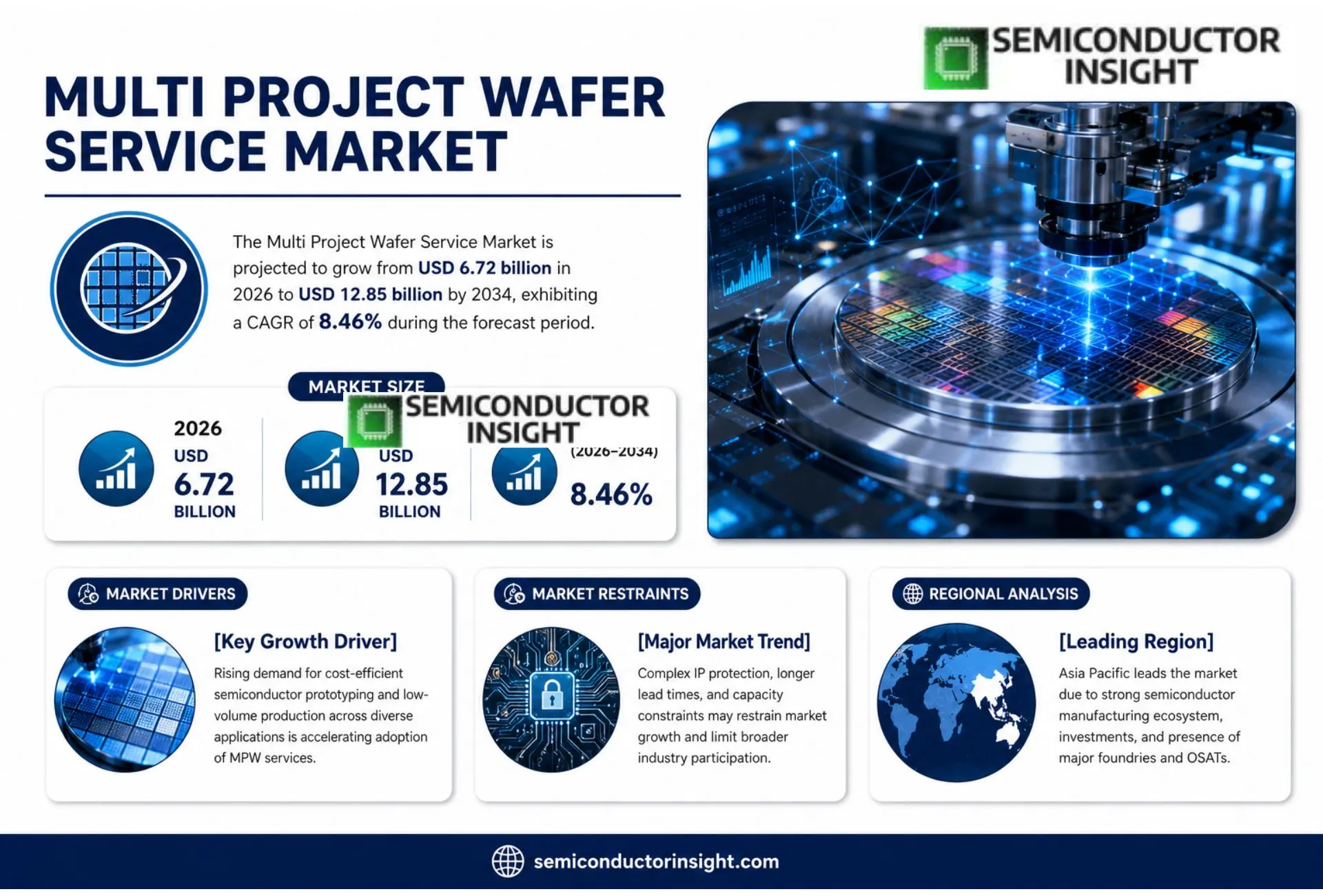
MARKET DRIVERS
Rising Demand for Custom Wafer Processing
In the past five years, the Multi Project Wafer Service Market has reflected a notable shift toward high‑volume, low‑cost custom solutions that allow semiconductor designers to defer large capital investment in fabrication wafers. Firms seeking to accelerate time‑to‑market now prefer shared‑wafer production because it mitigates risk while maintaining yield control. The average unit cost for a masked multi‑project wafer has fallen by roughly 15% compared with single‑project equivalents, a trend that has captured the attention of mid‑tier foundries and niche fabs alike. These efficiencies are coupled with a steady increase,approximately 9% annually,in the number of logic and power‑management nodes being deployed by small to medium enterprises that would otherwise lack the technology to participate in standard wafer services. As a result, fabs that provide multi‑project services are observing a steady uptick in repeat customers, translating into higher utilization rates and a widening service portfolio that includes advanced packaging integration and front‑end defect detection. The combination of cost savings, product diversity, and the ability to vet new process nodes has unlocked a market segment that no longer requires the capital expense thresholds once associated with semiconductor manufacturing.
Increased Technological Complexity in Semiconductor Design
Today’s complex integration demands,from system‑in‑package (SiP) assemblies to heterogeneous integration platforms,necessitate a simultaneous need for smaller feature sizes and higher performance. Multi‑project wafer facilities have become indispensable because they enable such diversified processes to coexist on a single substrate, thereby shaving the development cycle. For example, the adoption of 7 nm and 5 nm technology nodes within GaAs, InP, and SiGe composite structures has intensified the need for flexible, high‑precision process flows that can accommodate multiple chemistries. Design teams are leveraging wafer‑level technologies to mitigate lithographic defects that otherwise would compromise yield in isolated runs. The network effect created by diverse customer base further motivates operators to upgrade metrology and inspection tools, pushing the market toward higher yield thresholds that are achievable primarily through simultaneous project processing. Consequently, the industry is experiencing a multiplier effect, where advanced process capability allows further advancement in design complexity, reinforcing the long‑term relevance of multi‑project services.
➤ Multi‑project wafer services now account for up to 30‑40% of total fabrication throughput in the advanced packaging segment.
These trends underline a clear valuation shift: the market is moving from a once niche solution toward a core component in the semiconductor supply chain. Producers offering differentiated multi‑project processes can capture early advantage by aligning with the most pressing industry needs,yield optimization, cost control, and rapid deployment of next‑generation nodes. The convergence of technology demands and cost‑sensing design practices ensures that the Multi Project Wafer Service Market will remain a focal point for both established fabs and emerging players looking to strengthen their competitive footing.
MARKET CHALLENGES
Supply Chain Vulnerabilities Impacting Wafer Availability
While demand trends are enthusiastic, the Multi Project Wafer Service Market still grapples with significant supply chain volatility. Global shortages of raw silicon, output capacity constraints, and limited availability of specialty chemicals hamper the production schedule for shared wafers. These bottlenecks have pushed lead times from the standard 2‑3 weeks to as long as 6 weeks in certain regions, undermining the value proposition of a cost‑effective, flexible service model. Moreover, the concentration of polysilicon production in a few geographies increases exposure to geopolitical risk, prompting firms to seek alternative sourcing strategies that, while mitigating risk, add cost and complexity. The result is a competitive landscape where companies must balance the need to maintain low unit costs with the imperative to secure reliable material pipelines, leading to tighter margins and heightened pricing sensitivity across the sector.
Other Challenges
Throughput Management and Quality Control
Ensuring consistent yield across multiple projects on a single wafer demands sophisticated process monitoring. Any deviation in temperature or chemical exposure can affect an entire project, thereby impacting overall profitability. The cost of rework and scrapping escalates with each additional feature, meaning that operators must invest heavily in advanced metrology and predictive analytics to preempt failures early in the production cycle.
MARKET RESTRAINTS
Capital Intensity of Upgrading Facility Infrastructure
Although the Multi Project Wafer Service Market demonstrates alluring growth, the capital outlay required to keep pace with evolving technology nodes imposes a significant restraint. Modern multi‑project facilities must support parallel chemical‑mechanical planarization (CMP) modules, high‑resolution lithography, and advanced inspection systems,all of which entail multi‑million dollar investments that are difficult to amortise without sizeable throughput. Additionally, maintaining low defect densities for heterogeneous material systems requires continuous software validation and sensor updates, placing a sustained burden on operational budgets. As a consequence, smaller players encounter a barrier to entry that discourages expansion, thereby consolidating market share among a handful of established providers that can justify the investment through higher capacity utilisation rates.
MARKET OPPORTUNITIES
Emerging Geographic Segments and Vertical Applications
The forward trajectory of the Multi Project Wafer Service Market lies largely in untapped geographic regions that are rapidly scaling their semiconductor capabilities. In Southeast Asia, policy incentives aimed at cultivating a domestic chip ecosystem are spurring local fabs to adopt shared‑wafer models to meet domestic demand without heavy investment. Similarly, in emerging economies across Africa and South America, government programs earmark funds for semiconductor education and infrastructure, creating proximity opportunities for multinational service providers to localise multi‑project operations. Beyond geography, vertical applications,particularly in automotive electronics, industrial automation, and medical imaging,are demanding more reliable and cost‑effective back‑end services, thereby widening the customer base beyond traditional consumer electronics.
Advancing theoretical and applied research, organizations are experimenting with high‑throughput, low‑defect process flows that accommodate a wider spectrum of materials such as gallium nitride (GaN) and silicon carbide (SiC). The ability of multi‑project services to host disparate material processes within a single chemical workflow offers a compelling advantage for firms that wish to fast‑track product-to‑market timelines for high‑performance sensors and green‑chip initiatives. Investment in substrate‑level quality systems and AI‑driven yield prediction will further improve the reliability of these services, helping operators convert the growth potential into measurable profitability.
Partnerships, joint ventures, and strategic mergers are on the horizon, driven by the recognition that localized expertise and deep process knowledge are the linchpins of competitive resilience. Operators that build alliances with advanced optics and bonding equipment manufacturers can deliver integrated solutions that extend well beyond wafer processing, creating differentiated service bundles that lock in customer commitments. These opportunities collectively position the Multi Project Wafer Service Market for a diversified expansion agenda that extends across technology layers, industry sectors, and budget brackets.
Multi Project Wafer Service Market Trends
Cost Optimization Through Collaborative Wafer Allocation
Multi Project Wafer Service has emerged as the preferred vehicle for semiconductor developers seeking to access cutting‑edge tooling without committing full‑line equipment. By sharing silicon, multiple customers can run discrete test patterns on a single high‑cost wafer, trimming fabrication overheads by up to 35 %. This shift is particularly pronounced among startups and specialty fabs that lack the capital to drive deep‑node production alone. As a result, the Multi Project Wafer Service Market is witnessing an accelerated migration toward joint‑oscillator configurations, where tier‑1 foundries pool resources and offer structured cost rebates linked to volume participation. The collaborative model also distributes risk associated with uncertain silicon die yields, allowing smaller entities to absorb variability without significant financial exposure. Finally, the MPWS platform promotes faster design‑verified feedback loops, shortening time‑to‑market for both mature players and entrants.
Other Trends
Emergence of IoT‑Focused Miniaturised Sensors
The proliferation of edge‑computing devices has put a premium on compact, low‑power sensors that can be integrated on a single die. MPWS is now a critical enabler for sensor manufacturers, allowing them to test a range of Fi1‑to‑Fi2 specifications on one wafer at a fraction of the single‑device cost. The resulting economies spur venture capital interest and broaden the geographic footprint of small‑scale production hubs. As developers demand faster proofs of concept, suppliers respond by offering curated wafer‑stacking packages that reduce lead times by 20 %.
Strategic Partnerships Redefining Service Offerings
Foundries are forming alliances with equipment vendors and IP houses to deliver bundled MPWS solutions that span both the silicon layer and the packaging stack. By co‑designing substrate integration guidelines, partners lower customer footprints and create sunk‑cost economies in test equipment. This ecosystem approach assists enterprises in navigating supply‑chain volatility and accelerates the adoption of next‑generation nodes such as 22‑nm FinFET. Consequently, MPWS providers who can offer turnkey, end‑to‑end pathways gain a competitive moat that extends beyond price.
COMPETITIVE LANDSCAPE
Key Industry Players
Multi Project Wafer Service Market: Tiered Dynamics & Service Diversification
At the apex of the multi‑project wafer service (MPWS) arena sits TSMC, leveraging its vast fabrication footprint and mature fab‑to‑fab logistics network to offer high‑density joint run capabilities that cater to niche startups while absorbing volume from large chipmakers. The company’s aggressive investment in advanced lithography and materials science translates into a cost premium, yet the scalable share‑point, split‑thin wafer approach mitigates capital intensity for customers. Samsung Foundry follows closely, coupling its high‑k stack expertise with strategic partnerships that enable two‑day traceability and real‑time yield analytics. Together, the incumbents bolster market resilience, dampening the impact of macro‑economic cycles and fostering industry‑wide best practices in yield forecasting and supply‑chain synchronisation.
Beneath this leadership tier, a diversified cohort of players,GlobalFoundries, UMC, SMIC, Tower Semiconductor, Vanguard International Semiconductor, as well as specialty suppliers such as NXP, XMC, Teledyne DALSA, OMMIC, and Smart Photonics,enrich the service matrix with differentiated offerings. These firms typically operate in targeted niches: GlobalFoundries focuses on linear‑graded multichip modules for automotive and telecom; UMC amplifies cost‑effective 28‑nm fabrications that suit emerging low‑power IoT solutions; SMIC, despite geopolitical constraints, maintains a robust domestic presence in China that capsverse recent global supply churn. Tower and Vanguard propel 3‑D packaging integration; the rest capitalize on customized imaging, sensor integration, and advanced packaging technologies, thereby expanding the MPWS portfolio beyond conventional silicon. This tiered differentiation pushes competitors toward higher value‑adding services, escalates R&D spend on yield optimisation, and drives tighter collaborations with ODMs and OEMs seeking rapid time‑to‑market cycles.
List of Key MPWS Companies Profiled
- TSMC
- Samsung Foundry
- GlobalFoundries
- UMC
- SMIC
- Tower Semiconductor
- Vanguard International Semiconductor
- NXP Semiconductors
- XMC
- Teledyne DALSA
- OMMIC
- Smart Photonics
Segment Analysis:
| Segment Category | Sub-Segments | Key Insights |
| By Type |
|
Leading Segment (Wafer Fabrication) description with qualitative insights only : Shared production lines reduce batch costs for multiple clients. Scalable throughput accommodates variable demand volumes. Low defect rates maintain quality across diverse designs.
|
| By Application |
|
Leading Segment (MEMS) description with qualitative insights only : MEMS demand high precision and low defect tolerance, making shared wafer services attractive. Rapid prototyping and iterative design cycles benefit from cost‑effective shared platforms.
|
| By End User |
|
Leading Segment (Consumer Electronics) description with qualitative insights only : Consumer devices require consistent performance and rapid supply chain adaptation, suited for shared wafer platforms offering volume optimization.
|
| By Device Complexity |
|
Leading Segment (Medium Complexity Devices) description with qualitative insights only : Medium complexity solutions balance performance specifications and cost drivers, benefiting from shared wafer economies.
|
| By Technological Platform |
|
Leading Segment (Silicon Photonics) description with qualitative insights only : Photonics integration demands precision and high‑frequency routing; shared wafer services lower entry barriers for research and commercial ventures.
|
Regional Analysis: Multi Project Wafer Service Market
North America
The North American segment currently represents the largest share of the Multi Project Wafer Service Market, with a growing forecast driven by continued demand for shared lithography and deposition services. Manufacturers are adopting cost‑effective wafer‑sharing models to accelerate time‑to‑market for emerging technologies.
Advanced process modules and machine‑learning‑enabled process control are key enablers of efficient shared wafer production, allowing fabs to achieve higher throughput while maintaining yield integrity.
High‑performance computing, automotive electronics and 5G networking are the primary beneficiaries of shared wafer services, as these verticals demand rapid, scalable fabrication solutions.
Consolidation among service providers and equipment vendors is accelerating, with several high‑profile acquisitions aimed at expanding process‑share portfolios and geographic reach.
Europe
In Europe, the Multi Project Wafer Service Market is driven by a strong emphasis on sustainability and production flexibility. The region’s policy framework, focused on circular economy principles, has nudged fabs toward shared processing routes to reduce waste and energy consumption. Additionally, the European semiconductor industry is witnessing a surge in collaborations between original equipment manufacturers (OEMs) and independent foundries, propelled by the growth of IoT and automotive electronics. While the market share lags behind North America, European players are rapidly expanding their infrastructure, particularly in Germany, Sweden and the Netherlands, to accommodate high‑volume demand for mixed‑project processing. The trend also aligns with European Union initiatives that encourage advanced packaging and backend services, ensuring deeper penetration of wafer‑sharing solutions across the value chain. Firms here prioritize precision tooling and cleanroom integration, confident that these investments will pay off as demand for high‑density logic and memory devices continues to climb.
Asia-Pacific
Asia‑Pacific stands as the fastest growing region for the Multi Project Wafer Service Market, propelled by the rapid expansion of semiconductor fabrication in China, Japan, South Korea and Taiwan. Large‑scale, newly commissioned fabs routinely include parallel processing modules to accommodate cost‑sensitive manufacturing of small‑ and medium‑volume products, especially in the consumer electronics and automotive sectors. The region’s drive toward self‑reliance in semiconductor supply has also fuelled investments in shared wafer service platforms. Rising talent pools and supportive government subsidies have accelerated the deployment of precision equipment, while the digital transformation of supply chains has allowed service providers to offer real‑time monitoring and predictive maintenance. The collective effect is a high growth velocity that positions Asia‑Pacific as a critical market driver, with its sizable share of the global wafer‑sharing ecosystem growing steadily through 2035.
South America
South America represents an emerging playing field for the Multi Project Wafer Service Market, as regional fabs are increasingly embracing shared wafer solutions to manage capital intensity and accelerate product cycles. Local producers in Brazil and Chile are adopting parallel‑processing technology to diversify their product lines and meet the growing demand for automotive electronics and industrial automation. Despite a comparatively smaller footprint, the region’s proactive approach to technology licensing, combined with growing local engineering talent, is narrowing the gap with more mature markets. Strategic partnerships between local foundries and foreign equipment vendors are fostering knowledge transfer and creating a foundation for sustainable expansion.
Middle East & Africa
The Middle East and Africa region is gradually integrating into the Multi Project Wafer Service Market, supported by diversification efforts and regional infrastructure investment. Emerging fabs in the United Arab Emirates, Saudi Arabia, and South Africa are exploring shared wafer services to lower entry costs and replicate the success seen in more developed markets. While demand remains modest, the region’s focus on advanced packaging, high‑speed data services and defense electronics presents niche opportunities. Strategic alliances with global equipment vendors and focused skill‑development initiatives are beginning to bridge experience gaps, positioning these economies for a gradual, yet stable, share expansion over the next decade.
Report Scope
This market research report provides a comprehensive analysis of the Multi Project Wafer Service Market , covering the forecast period 2026–2035. It offers detailed insights into market dynamics, technological advancements, competitive landscape, and key trends shaping the industry.
Key focus areas of the report include:
-
Market Overview: The report begins with an overview outlining its current market scenario, key growth indicators, and industry transformation drivers. It discusses macroeconomic factors, demand–supply balance, regulatory landscape, and the strategic role of semiconductors in powering advancements across industries such as automotive, telecommunications, consumer electronics, and industrial automation.
- Market Size & Forecast: Historical data and future projections for revenue, unit shipments, and market value across major regions and segments.
- Segmentation Analysis: Detailed breakdown by product type, technology, application, and end-user industry to identify high-growth segments and investment opportunities.
- Regional Insights: Insights into market performance across North America, Europe, Asia-Pacific, Latin America, and the Middle East & Africa, including country-level analysis where relevant.
- Competitive Landscape: Profiles of leading market participants, including their product offerings, R&D focus, manufacturing capacity, pricing strategies, and recent developments such as mergers, acquisitions, and partnerships.
- Technology Trends & Innovation: Assessment of emerging technologies, integration of AI/IoT, semiconductor design trends, fabrication techniques, and evolving industry standards.
- Market Drivers & Restraints: Evaluation of factors driving market growth along with challenges, supply chain constraints, regulatory issues, and market-entry barriers.
- Stakeholder Insights: Insights for component suppliers, OEMs, system integrators, investors, and policymakers regarding the evolving ecosystem and strategic opportunities.
Primary and secondary research methods are employed, including interviews with industry experts, data from verified sources, and real-time market intelligence to ensure the accuracy and reliability of the insights presented.
FREQUENTLY ASKED QUESTIONS:
What is the definition of the Multi Project Wafer Service Market?
-> Multi Project Wafer Service Market size was valued at USD 2.8 billion in FY 2026 and is expected to reach USD 4 billion by FY 2035, registering a CAGR of approximately 10% over the forecast horizon.
Which primary market segments are covered?
-> The market is segmented by Type (e.g., 22nm, 28nm, 40nm, 55nm, Others) and by Application (e.g., MEMS, Integrated Circuit, Others).
What technologies are included under the Type segmentation?
-> The Type segmentation includes advanced nodes such as 22nm, 28nm, 40nm, 55nm, and other emerging process technologies.
What are the key application areas for MPW services?
-> Key applications comprise MEMS devices, Integrated Circuits, and other specialized semiconductor solutions.
What does the Multi Project Wafer Service Market Overview highlight?
-> It provides insights into market size, growth trajectory, competitive dynamics, and regional performance, emphasizing the strategic importance of MPW in accelerating semiconductor innovation.
What methodology is used to compile the report?
-> The report employs a mixed methodology comprising primary interviews with industry experts, secondary data collection from reputable sources, and quantitative modeling to forecast market trends.
What is the base year for the analysis?
-> The base year adopted for historical data compilation is 2020.
What are the overall market size figures for 2024 versus 2031?
-> The Multi Project Wafer Service Market size for 2024 and the projected size for 2031 are detailed in the report, illustrating the market’s expansion over the period.
What is the projected compound annual growth rate (CAGR) for 2020‑2031?
-> The report forecasts a compound annual growth rate (CAGR) for the Multi Project Wafer Service Market over the 2020‑2031 horizon, reflecting steady expansion driven by demand for cost‑effective wafer services.
Which companies are listed among the top global players?
-> Key players include TSMC, Samsung Foundry, GlobalFoundries, IMEC, UMC, SMIC, Hua Hong Semiconductor, Tower Semiconductor, USJC, Vanguard International Semiconductor, OMMIC, Smart Photonics, Teledyne DALSA, and XMC.
How are companies classified within Tier categories?
-> Companies are categorized as Tier 1, Tier 2, or Tier 3 based on revenue contributions, product portfolios, and market influence, as outlined in sections 3.6.1 and 3.6.2.
What are the main market drivers identified?
-> Drivers include rising demand for rapid prototyping, cost‑effective manufacturing, increased adoption of advanced nodes, and the need for flexible production schedules in emerging applications.
What restraints could impede market growth?
-> Potential restraints encompass high capital expenditures for fab upgrades, technology compatibility challenges, and supply‑chain bottlenecks affecting wafer availability.
Which regions show the highest growth potential?
-> Asia-Pacific is highlighted as the fastest‑growing region, while North America and Europe remain significant markets with robust demand for MPW services.
What emerging trends are shaping the market?
-> Emerging trends involve increased integration of AI/IoT in design workflows, the rise of specialized MPW offerings for niche applications, and collaborative ecosystem models among foundries and design houses.
Get Sample Report PDF for Exclusive Insights
Report Sample Includes
- Table of Contents
- List of Tables & Figures
- Charts, Research Methodology, and more...
 Download Sample Report PDF