
Microbump (Cu/SnAg) Advanced Plating Market Insights
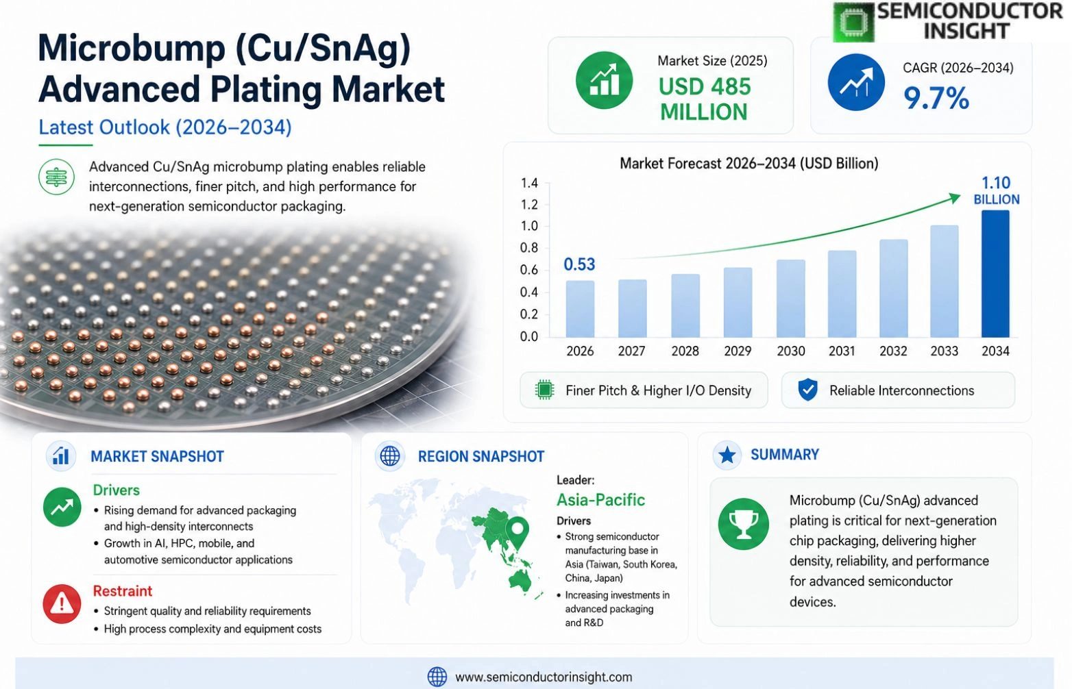
Global Microbump (Cu/SnAg) Advanced Plating Market size was valued at USD 485 million in 2025. The market is projected to grow from USD 530 million in 2026 to USD 1.1 billion by 2034, exhibiting a CAGR of 9.7% during the forecast period.
Microbumps, specifically copper-tin-silver (Cu/SnAg) advanced plating, are ultra-fine interconnects used primarily in semiconductor packaging and heterogeneous integration. These micro-scale bumps enable high-density chip stacking and enhanced electrical performance, making them critical for advanced packaging technologies such as flip-chip, fan-out wafer-level packaging (FOWLP), and 2.5D/3D IC integration. The Cu/SnAg plating process ensures reliable bonding with superior thermal and electrical conductivity, addressing the growing demand for miniaturization, higher I/O density, and improved signal integrity in next-generation electronics.
The rapid expansion of the market is driven by the surging adoption of high-performance computing (HPC), artificial intelligence (AI) chips, and advanced driver-assistance systems (ADAS). Furthermore, the shift toward chiplet-based architectures and the proliferation of 5G infrastructure are accelerating demand for high-reliability microbumps. Leading semiconductor manufacturers are investing heavily in R&D to optimize Cu/SnAg plating processes for finer pitch sizes below 30 micrometers, ensuring compatibility with emerging packaging roadmaps.
MARKET DRIVERS
DRIVE TOWARDS HETEROGENEOUS INTEGRATION
The rapid expansion of Microbump (Cu/SnAg) Advanced Plating Market is fundamentally anchored by the industry’s pivot toward 2.5D and 3D packaging architectures. As die sizes shrink and interconnect density increases, the demand for high-reliability, small-pitch interconnects has necessitated the adoption of Cu/SnAg microbumps over traditional copper pillars, facilitating greater bandwidth and performance.
ENHANCED THERMAL AND MECHANICAL PERFORMANCE
Copper-Sn-Ag stacks offer superior mechanical strength and lower electrical resistivity compared to pure copper. This makes them ideal for high-speed data transmission and power management applications within advanced semiconductor packages, ensuring signal integrity under high operational loads.
➤ Superior reliability under thermal cycling conditions remains a primary catalyst for growth.
The push for energy-efficient electronics drives the need for solder materials that ensure reliable interconnects without excessive thermal stress, further solidifying the demand for Cu/SnAg solutions.
MARKET CHALLENGES
PROCEDURAL COMPLEXITY IN NANOSCALE DEPOSITION
Depositing Cu/SnAg microbumps with high uniformity at the wafer-level requires sophisticated electroplating techniques that are difficult to scale consistently across large substrates, creating bottlenecks for high-volume manufacturing.
Other Challenges
Interface Reliability
Thermomechanical stress at the interface between the Cu/SnAg bumps and the underlying silicon chip can lead to potential failure mechanisms over time if not properly managed.
MARKET RESTRAINTS
HIGH INITIAL CAPITAL INFRASTRUCTURE
Establishing a fabrication line capable of handling Cu/SnAg electroplating processes requires substantial capital investment in specialized plating equipment and vacuum chambers, which can be a deterrent for smaller operations.
Additionally, the maintenance of plating bath chemistries is expensive and time-consuming, increasing the overall cost of production.
MARKET OPPORTUNITIES
EXPANSION INTO AUTOMOTIVE ELECTRONICS
The increasing requirement for robust, high-temperature packaging in ADAS and EV applications offers a significant growth avenue for advanced plating technologies that can withstand harsh environmental conditions.
The growing demand for specialized plating slurries tailored specifically to Cu/SnAg recipes represents an emerging service and product opportunity.
Trends
Expansion of Heterogeneous Integration and Miniaturization
Microbump (Cu/SnAg) Advanced Plating Market is experiencing robust growth driven by the critical requirement for heterogeneous integration in next-generation electronics. Advanced plating using copper-tin-silver alloys provides essential ultra-fine interconnects that possess superior thermal and electrical conductivity, making them indispensable for modern semiconductor packaging. These micro-scale bumps facilitate high-density chip stacking, which directly supports complex 2.5D and 3D IC architectures. As the industry aggressively pursues finer pitches and increased I/O densities, advanced packaging technologies such as flip-chip and fan-out wafer-level packaging rely heavily on this reliability. The continuous trend toward miniaturization ensures that signal integrity is maintained under high operational stress, solidifying the role of Cu/SnAg plating as a foundational enabler for sophisticated electronic systems.
Other Trends
Acceleration Driven by AI and 5G Infrastructure
The trajectory of the market is inextricably linked to the rapid expansion of high-performance computing and artificial intelligence infrastructure. Modern AI and HPC chips require interconnects capable of handling immense data throughput, creating a significant demand for microbumps that support the highest possible density. This need is further bolstered by the widespread deployment of 5G infrastructure and the proliferation of advanced driver-assistance systems, both of which necessitate microbumps providing high reliability and low latency. Additionally, the growing adoption of chiplet-based architectures presents a substantial trend, as these modular designs require highly consistent and reliable bonding processes to function correctly across diverse specialized compute units.
Process Optimization and Roadmap Compatibility
Looking ahead, competition among leading players is intensifying as they strive to refine the Cu/SnAg plating process to support emerging packaging roadmaps. Current strategic focus areas include the development of finer pitch technologies below 30 micrometers to meet the rigorous demands of next-generation consumer electronics and automotive systems. Continuous investment in R&D aims to enhance the bond strength and thermal reliability of these microbumps, addressing the specific challenges associated with miniaturization. By ensuring compatibility with evolving node geometries, manufacturers are positioning themselves to capitalize on the sustained market expansion driven by sophisticated electronic applications and the relentless push for higher performance.
COMPETITIVE LANDSCAPE
Key Industry Players
Market Expansion Driven by Demand for Heterogeneous Integration
The global Microbump (Cu/SnAg) Advanced Plating Market is a critical segment within the semiconductor ecosystem, valued at USD 485 million in 2025 and expected to surge to USD 1.1 billion by 2034. Market analysts project a compound annual growth rate (CAGR) of 9.7%, driven by the escalating demand for advanced packaging technologies that enable high-density chip stacking and enhanced electrical performance in next-generation electronics.
The competitive landscape is defined by leaders who are investing significantly in R&D to optimize Cu/SnAg plating processes. These manufacturers are addressing the challenges of miniaturization to support flip-chip and fan-out wafer-level packaging, ensuring superior thermal conductivity and signal integrity for high-performance computing, AI chips, and 5G infrastructure applications.
List of Key Advanced Plating Technology Companies Profiled
- Tokyo Electron
- ASM Pacific Technology
- Heraeus Holding
- Entegris
- Schmid Group
- K&S
- Ebara
- Hitachi High-Technologies
- ULVAC
- Fujifilm Corporation
- Disco Corporation
- Nexolve (Dow)
Segment Analysis:
| Segment Category | Sub-Segments | Key Insights |
| By Type |
|
Electroless Cu/SnAg leads due to superior uniformity on complex 3D structures, which is critical for heterogeneous integration and fine pitch requirements in advanced chip architectures. |
| By Application |
|
Flip-Chip and FOWLP applications dominate the landscape. These technologies rely on robust Cu/SnAg bonds to ensure thermal expansion compatibility and prevent signal fatigue in high-performance computing environments. |
| By End User |
|
HPC and AI sectors are the primary drivers, demanding ultra-fine bumps to handle increased I/O density and signal integrity requirements associated with sophisticated AI accelerators. |
| By Plating Technology |
|
Sub-Micron Pitch Processing is becoming the benchmark for advanced packaging. The competitive landscape is shifting toward processes capable of maintaining structural integrity under extreme thermal stress during subsequent lamination steps. |
| By Pitch Size Requirement |
<li>30-50 micrometer=”” pitch=””>
</li>30-50> |
The <30 Micrometer segment represents the highest growth potential. The race for miniaturization in next-generation electronics is forcing manufacturers to refine Cu/SnAg plating processes to ensure conductivity without compromising mechanical reliability. |
Regional Analysis: Microbump (Cu/SnAg) Advanced Plating Market
Asia-Pacific
Major semiconductor foundries in the region are aggressively expanding their manufacturing facilities, creating a substantial surge in demand for high-volume Cu/SnAg microbump plating materials to directly support their advanced 3D IC stacking capacity requirements.
The sheer scale of mobile device manufacturing in Asian economies forces rapid evolution cycles, continuously raising the bar for micro-bump density and necessitating superior plating chemistries to manage the thermal loads of next-gen smartphones and wearables.
Beyond consumer goods, the region serves as a powerhouse for high-performance computing and automotive manufacturing, where the specific mechanical properties of Copper-Silver-Tin (Cu/SnAg) alloys are critical for maintaining signal integrity in dense interconnect structures.
A strategic vertical integration trend by local chipmakers is reducing reliance on external component suppliers, creating a stable and efficient environment for the domestic production and rapid deployment of advanced plating solutions.
North America
The North American market is primarily driven by leadership in research and development, particularly within the autonomous vehicle and aerospace sectors. Here, the adoption of Microbump (Cu/SnAg) Advanced Plating is necessitated by a demand for extreme reliability and high thermal endurance. The region’s manufacturers prioritize advanced plating solutions that ensure signal integrity and prevent connection failures under the rigorous operating conditions inherent to aviation and autonomous driving technologies.
Europe
Europe maintains a robust demand for these advanced metallurgical solutions, largely due to its strong heritage in automotive manufacturing and industrial automation. The European market benefits from standardized testing protocols that favor the specific mechanical characteristics of Cu/SnAg alloys, which offer excellent fatigue resistance and thermal cycle performance. As the regulatory pressure mounts for energy efficiency in industrial electronics, the need for reliable micro-bumping becomes a critical differentiator for manufacturers in this region.
Asia-Pacific
Extending beyond the primary leadership perspective, the broader APAC market continues to exhibit significant growth momentum driven by regional semiconductor foundries and government initiatives aimed at boosting local electronics production capacity through advanced packaging technologies. The region acts as a testbed for new 2.5D and 3D integration techniques, fostering an environment where innovative plating methods can be quickly refined and scaled before reaching global markets.
South America
While currently representing a smaller fraction of the global footprint, South America is observing a gradual but steady uptake of these technologies to support the expansion of its domestic automotive industry and increasing integration of digital infrastructure. The market dynamics here are shifting from basic connectivity to more complex high-end electronic systems, requiring the enhanced reliability offered by advanced plating processes to support local industrialization goals.
Middle East & Africa
The market in this region is in a developmental stage; however, the pace of digital transformation is beginning to catalyze the demand for advanced plating solutions. Investment in modernizing industrial infrastructure is slowly translating into a requirement for high-performance micro-bumps, although the application currently remains concentrated within high-value telecommunication and governmental projects rather than consumer electronics.
Report Scope
This market research report provides a comprehensive analysis of the Microbump (Cu/SnAg) Advanced Plating Market , covering the forecast period 2026–2034. It offers detailed insights into market dynamics, technological advancements, competitive landscape, and key trends shaping the industry.
Key focus areas of the report include:
- Market Overview: The report begins with an overview outlining its current market scenario, key growth indicators, and industry transformation drivers. It discusses macroeconomic factors, demand–supply balance, regulatory landscape, and the strategic role of semiconductors in powering advancements across industries such as automotive, telecommunications, consumer electronics, and industrial automation.
- Market Size & Forecast: Historical data and future projections for revenue, unit shipments, and market value across major regions and segments.
- Segmentation Analysis: Detailed breakdown by product type, technology, application, and end-user industry to identify high-growth segments and investment opportunities.
- Regional Insights: Insights into market performance across North America, Europe, Asia-Pacific, Latin America, and the Middle East & Africa, including country-level analysis where relevant.
- Competitive Landscape: Profiles of leading market participants, including their product offerings, R&D focus, manufacturing capacity, pricing strategies, and recent developments such as mergers, acquisitions, and partnerships.
- Technology Trends & Innovation: Assessment of emerging technologies, integration of AI/IoT, semiconductor design trends, fabrication techniques, and evolving industry standards.
- Market Drivers & Restraints: Evaluation of factors driving market growth along with challenges, supply chain constraints, regulatory issues, and market-entry barriers.
- Stakeholder Insights: Insights for component suppliers, OEMs, system integrators, investors, and policymakers regarding the evolving ecosystem and strategic opportunities.
Primary and secondary research methods are employed, including interviews with industry experts, data from verified sources, and real-time market intelligence to ensure the accuracy and reliability of the insights presented.
FREQUENTLY ASKED QUESTIONS:
What is the current market size of Microbump (Cu/SnAg) Advanced Plating Market?
-> Microbump (Cu/SnAg) Advanced Plating Market size was valued at USD 485 million in 2025. The market is projected to grow from USD 530 million in 2026 to USD 1.1 billion by 2034, exhibiting a CAGR of 9.7% during the forecast period.
Which key companies operate Microbump (Cu/SnAg) Advanced Plating Market?
-> Key players include Axalta Coating Systems, AkzoNobel, BASF SE, PPG, Sherwin-Williams, and 3M, among others.
What are the key growth drivers?
-> Key growth drivers include high-performance computing (HPC), artificial intelligence (AI) chips, advanced driver-assistance systems (ADAS), and 5G infrastructure proliferation.
Which region dominates the market?
-> Asia-Pacific is the fastest-growing region, while Europe remains a dominant market.
What are the emerging trends?
-> Emerging trends include finer pitch microbumps (<30 micrometers), 2.5D/3D IC integration, and fan-out wafer-level packaging (FOWLP).

Get Sample Report PDF for Exclusive Insights
Report Sample Includes
- Table of Contents
- List of Tables & Figures
- Charts, Research Methodology, and more...


