Memory Package Substrate Market Insights
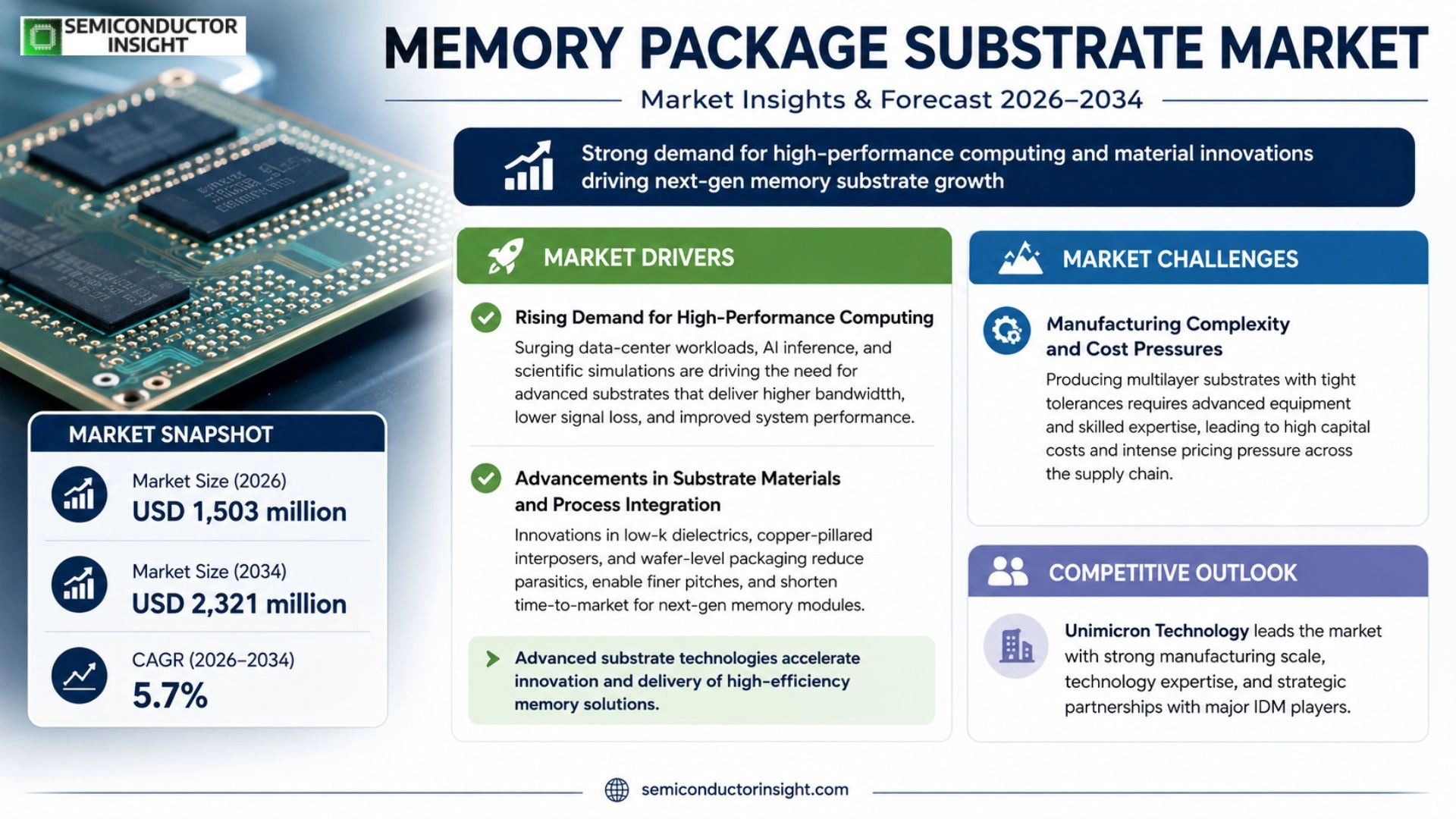
Memory Package Substrate market expands from USD 1,503 million in 2026 to USD 2,321 million by 2034, reflecting a CAGR of 5.7 % over the forecast period.
Memory package substrates, sometimes referred to as memory substrates, are semiconductor IC substrates that safeguard chips and furnish electrical connections for mounting on printed wiring boards. Core formats comprise wafer‑level chip‑scale packages (WBCSP), wafer‑level ball grid array (WB‑BGA) and flip‑chip CSP (FCCSP), serving DRAM, NAND flash and related SSD, embedded storage and mobile memory applications. Demand accelerates alongside AI‑driven computing, cloud services and the relentless miniaturisation of smartphones and wearables, compelling manufacturers toward higher density, multilayer and low‑profile solutions.
MARKET DRIVERS
Rising Demand for High‑Performance Computing
Memory Package Substrate Market is being propelled by the surge in data‑center workloads, AI inference, and scientific simulations that require ever‑faster memory interfaces. Chip manufacturers are turning to advanced substrate designs to minimise signal loss, a move that directly translates into higher throughput for server‑grade processors. This shift is not merely a technical preference; it enables customers to squeeze more performance from existing silicon, thereby extending the economic life of costly platforms.
Advancements in Substrate Materials and Process Integration
Recent breakthroughs in low‑k dielectric formulations and copper‑pillared interposers have lowered parasitic capacitance, allowing tighter pin pitches without compromising reliability. Coupled with the migration toward wafer‑level packaging, these material innovations reduce the number of assembly steps, which in turn trims cycle time. Companies that master this integration gain a competitive edge because they can deliver memory modules that meet the power‑efficiency targets set by OEMs.
➤ Integration of advanced substrate technologies shortens time‑to‑market for next‑gen memory modules.
Overall, the convergence of performance‑driven demand and material science progress creates a feedback loop: as customers ask for higher bandwidth, suppliers refine substrate processes, which then unlocks new product categories for Memory Package Substrate Market.
MARKET CHALLENGES
Manufacturing Complexity and Cost Pressures
Fabricating multilayer substrates that meet tight dimensional tolerances requires specialised equipment and highly skilled labour. The capital outlay for such lines can strain the balance sheets of mid‑size players, limiting their ability to scale. Consequently, price competition intensifies, forcing manufacturers to optimise yield through sophisticated defect‑detection algorithms and tighter process control.
Other Challenges
Supply‑Chain Volatility
The reliance on scarce raw materials such as high‑purity copper and specialty polymers makes the supply chain vulnerable to geopolitical shifts. When a key supplier faces export restrictions, lead times extend, and manufacturers are compelled to hold larger safety stocks, which erodes profitability in an otherwise marginal market.
MARKET RESTRAINTS
Limited Availability of Specialized Equipment
Only a handful of equipment vendors produce the high‑resolution lithography tools required for fine‑pitch substrate patterning. This bottleneck raises procurement lead times and leaves new entrants dependent on legacy machinery that cannot support the next wave of density demands.
Furthermore, the stringent thermal‑management standards imposed by automotive and aerospace customers add another layer of qualification. Meeting these standards often demands redesign of the substrate stack, which delays product introductions and inflates engineering budgets.
Lastly, environmental regulations concerning the disposal of epoxy‑based substrates increase compliance costs. Companies must invest in recycling infrastructure or face penalties, a factor that dampens aggressive expansion plans within Memory Package Substrate Market.
MARKET OPPORTUNITIES
Emergence of Chip‑Scale Packaging for AI Accelerators
AI accelerators rely on ultra‑low latency memory stacks, and chip‑scale packaging (CSP) offers an optimal route to achieve that performance envelope. Substrate technologies that enable direct‑bond interconnects are positioned to capture a growing slice of Memory Package Substrate Market as AI workloads become mainstream across cloud and edge environments.
Geographically, Southeast Asian manufacturing hubs are expanding their capabilities to support high‑volume substrate production, attracted by favorable trade policies and a skilled workforce. This regional shift opens avenues for partnerships and joint‑venture initiatives that can lower entry barriers for Western firms.
In addition, the rising adoption of 3D‑stacked memory in automotive infotainment and advanced driver‑assistance systems presents a niche yet lucrative opportunity. Substrate designs that accommodate higher thermal dissipation while maintaining thin form factors are likely to command premium pricing, driving margins for early adopters.
Memory Package Substrate Market Trends
High‑Density Substrate Demand Accelerates Market Momentum
The surge in high‑density memory applications is reshaping Memory Package Substrate Market. AI inference accelerators, cloud‑scale servers and next‑generation electric‑vehicle infotainment systems demand substrates that support eight or more routing layers while remaining thin enough for compact form factors. Miniaturized smartphones and wearable devices further compress the vertical space, forcing designers to adopt multilayer, low‑profile laminates. To meet these pressures, leading substrate makers are accelerating the rollout of fine‑pitch fabrication lines and investing in high‑modulus copper‑clad materials. Companies that can consistently deliver 8+ layer boards at target cost structures are positioning themselves to win strategic contracts from DRAM and NAND fabs, translating technical capability into market share gains. Furthermore, the migration to 3D‑stacked DRAM architectures intensifies the need for substrates that can accommodate TSV interposers without compromising mechanical stability, pushing vendors to explore glass‑based and organic‑inorganic hybrid laminates.
Other Trends
Impact of AI‑Driven Workloads on Substrate Architecture
AI‑driven workloads are tightening tolerances on signal integrity, which reverberates through the substrate stack‑up. Memory modules that feed deep‑learning accelerators must maintain low latency and minimal power loss, prompting a shift toward wafer‑level packaging formats such as WB‑CSP and FCCSP. These formats rely on tighter bump pitches and thinner dielectric layers, raising the importance of precise copper foil placement and advanced under‑fill chemistries. As a result, design houses are increasingly collaborating with substrate suppliers early in the product development cycle, sharing layout data to co‑optimize trace geometry and impedance. This collaborative model compresses time‑to‑market but also introduces pricing pressure, as customers expect cost parity with traditional BGA solutions. The pressure to reduce bump height also drives the adoption of lead‑free solder alloys, which, while environmentally favorable, demand tighter thermal profiles during reflow, adding another layer of complexity to the supply chain.
Regional Competition and Supply‑Chain Realignment
In spite of the technical convergence, the competitive landscape remains highly regional. Taiwan, South Korea, Japan and mainland China host the majority of high‑volume Memory Package Substrate producers, each leveraging localized silicon‑foundry ecosystems to secure supply agreements. Recent capacity expansions in the Asian corridor have been tempered by geopolitical frictions, prompting several OEMs to diversify suppliers toward emerging hubs in Southeast Asia and the United States. This rebalancing is reshaping pricing dynamics, with lead‑time premiums shrinking as alternative sources attain scale. For manufacturers, the imperative now is to secure raw‑material contracts, standardize process qualifications, and articulate clear value propositions that align with the evolving sourcing strategies of memory fabs. Operators that can demonstrate compliance with emerging environmental regulations while maintaining high yields will likely command premium pricing as customers increasingly factor sustainability into their supplier selection.
COMPETITIVE LANDSCAPE
Key Industry Players
Memory Package Substrate Competitive Outlook
Unimicron Technology continues to dominate the memory substrate arena, leveraging its extensive fab capacity and deep relationships with IDM chipmakers. Its portfolio spans WB‑CSP, WB‑BGA and FCCSP formats, allowing it to capture a disproportionate share of high‑density DRAM and NAND packaging contracts. The company’s aggressive scaling of multilayer stack processes has translated into a cost advantage that pressures smaller rivals, while its geographic footprint across Taiwan, China and Southeast Asia provides resilience against regional supply shocks. This concentration around a few large fabs creates a tiered market where Tier‑1 players negotiate long‑term supply agreements, leaving room for specialist firms to chase niche design wins.
Beyond the leader, the substrate space hosts a disparate set of manufacturers that compete on technology differentiation, regional proximity, or price efficiency. Samsung Electro‑Mechanics, Nan Ya PCB and Shinko Electric Industries each excel in specific form‑factor shipments, often serving domestic memory producers in South Korea, Taiwan and Japan. Zhen Ding Technology and Daeduck Electronics have invested heavily in 6‑layer and 8‑plus stack capabilities to serve AI‑focused server memory. LG InnoTek, DAISHO DENSHI, Korea Circuit and a host of Chinese outfits such as Shennan Circuit, Shenzhen Fastprint Circuit Tech, Shenzhen Hemei Jingyi Semiconductor Technology, Hong Yuen Electronics and Huizhou China Eagle Electronic Technology round out the competitive mix, each targeting particular segments from mobile memory to embedded storage. Their collective activity keeps the market fluid and offers customers alternatives to the dominant Tier‑1 supply chain.
List of Key Memory Package Substrate Companies Profiled
- Unimicron Technology
- Samsung Electro‑Mechanics
- Nan Ya PCB
- Shinko Electric Industries
- Zhen Ding Technology
- Daeduck Electronics
- LG InnoTek
- DAISHO DENSHI
- Korea Circuit
- Shennan Circuit
- Shenzhen Fastprint Circuit Tech
- Shenzhen Hemei Jingyi Semiconductor Technology
- Hong Yuen Electronics
- Huizhou China Eagle Electronic Technology
Segment Analysis:
| Segment Category | Sub-Segments | Key Insights |
| By Type |
|
WBCSP
|
| By Application |
|
Memory Modules
|
| By End User |
|
Consumer Electronics
|
| By Layer Count |
|
4‑6 layers
|
| By Product Form |
|
Flip Chip
|
Regional Analysis: Memory Package Substrate Market
Asia-Pacific
Foundries are repurposing legacy fabs to accommodate higher substrate throughput, leveraging modular equipment that can be swapped between standard and advanced packaging lines. This flexibility reduces capital lock‑in and aligns capacity with fluctuating memory demand cycles.
Collaborative labs in Shenzhen and Tokyo focus on embedding signal‑integrity enhancements directly into substrate layouts, a shift that diminishes the need for post‑fabrication tuning and shortens time‑to‑market for memory modules.
Multi‑sourcing strategies, backed by strategic stockpiles of high‑purity copper and epoxy, cushion the region against geopolitical shocks, ensuring uninterrupted substrate deliveries for high‑mix memory products.
Harmonized environmental standards across ASEAN and East Asia streamline compliance, allowing firms to adopt greener substrate chemistries without fragmenting their product portfolios.
North America
North America remains a pivotal market for memory substrate development, driven largely by the presence of leading design houses and a mature consumer electronics ecosystem. Companies here prioritize high‑performance substrate architectures that support demanding data‑center memory modules, emphasizing thermal management and high‑frequency signal routing. The region’s investment in advanced research facilities translates into early adoption of emerging packaging formats, prompting a ripple effect across the supply chain. However, stringent environmental regulations and an emphasis on cost transparency compel manufacturers to balance innovation with operational efficiency, shaping a market that favors strategic partnerships and joint‑venture models to share risk and accelerate time‑to‑revenue.
Europe
Europe’s Memory Package Substrate Market is characterized by a strong focus on precision engineering and sustainability. German and French fab operators are integrating additive manufacturing techniques into substrate production, targeting weight reduction and material savings for automotive memory applications. The regulatory environment, particularly the EU’s ecological directives, drives continuous improvement in substrate waste management, influencing supplier selection criteria. As automotive and industrial IoT segments expand, European firms are leveraging their expertise in high‑reliability substrates to capture niche opportunities, often through collaborative consortia that pool R&D resources across borders.
South America
In South America, the substrate market is still emerging but benefits from a growing consumer base and increasing local assembly of memory‑intensive devices. Brazil’s electronics clusters are attracting foreign substrate suppliers seeking proximity to end‑users, which shortens logistics and reduces lead times. While capital investment remains modest, regional governments are offering incentives for technology parks focused on advanced packaging, hinting at a gradual shift from low‑cost assembly to value‑added substrate manufacturing. The trajectory suggests a market that will move from import reliance toward modest domestic capability within the next decade.
Middle East & Africa
The Middle East & Africa region exhibits a modest yet strategically important presence in Memory Package Substrate Market. Investment funds from Gulf states are earmarking capital for semiconductor ecosystem development, with a particular interest in establishing test and packaging facilities that can serve both local and export markets. Africa’s nascent electronics sector is drawing attention for its potential in renewable‑energy‑linked memory solutions, prompting early‑stage collaborations focused on ruggedized substrates. While current volumes are limited, the region’s commitment to building a diversified tech portfolio positions it as a future growth corridor for specialized substrate applications.
Report Scope
This market research report provides a comprehensive analysis of the Memory Package Substrate Market , covering the forecast period 2026–2034. It offers detailed insights into market dynamics, technological advancements, competitive landscape, and key trends shaping the industry.
Key focus areas of the report include:
- Market Overview: The report begins with an overview outlining its current market scenario, key growth indicators, and industry transformation drivers. It discusses macroeconomic factors, demand–supply balance, regulatory landscape, and the strategic role of semiconductors in powering advancements across industries such as automotive, telecommunications, consumer electronics, and industrial automation.
- Market Size & Forecast: Historical data and future projections for revenue, unit shipments, and market value across major regions and segments.
- Segmentation Analysis: Detailed breakdown by product type, technology, application, and end-user industry to identify high-growth segments and investment opportunities.
- Regional Insights: Insights into market performance across North America, Europe, Asia-Pacific, Latin America, and the Middle East & Africa, including country-level analysis where relevant.
- Competitive Landscape: Profiles of leading market participants, including their product offerings, R&D focus, manufacturing capacity, pricing strategies, and recent developments such as mergers, acquisitions, and partnerships.
- Technology Trends & Innovation: Assessment of emerging technologies, integration of AI/IoT, semiconductor design trends, fabrication techniques, and evolving industry standards.
- Market Drivers & Restraints: Evaluation of factors driving market growth along with challenges, supply chain constraints, regulatory issues, and market-entry barriers.
- Stakeholder Insights: Insights for component suppliers, OEMs, system integrators, investors, and policymakers regarding the evolving ecosystem and strategic opportunities.
Primary and secondary research methods are employed, including interviews with industry experts, data from verified sources, and real-time market intelligence to ensure the accuracy and reliability of the insights presented.
FREQUENTLY ASKED QUESTIONS:
What is the current market size of Memory Package Substrate Market?
-> Memory Package Substrate market expands from USD 1,503 million in 2026 to USD 2,321 million by 2034, reflecting a CAGR of 5.7 % over the forecast period.
Which key companies operate in Memory Package Substrate Market?
-> Key players include Unimicron Technology, Samsung Electro-Mechanics, Nanya PCB, Shinko Electric Industries, Zhen Ding Technology, Daeduck Electronics, LG InnoTek, Shennan Circuit, Shenzhen Fastprint Circuit Tech, Shenzhen Hemei Jingyi Semiconductor Technology, Hong Yuen Electronics, Huizhou China Eagle Electronic Technology.
What are the key growth drivers?
-> Key growth drivers include the demand for high‑speed, high‑integration and low‑power ICs, rapid advancements in AI, cloud computing, intelligent automotive applications, and the miniaturization and thinning of smartphones and wearable devices that require high‑density, multilayer, low‑profile memory substrates.
Which region dominates the market?
-> Asia dominates Memory Package Substrate market, with significant activity in China, Taiwan, South Korea, and Japan.
What are the emerging trends?
-> Emerging trends include the adoption of advanced memory substrate technologies such as WBCSP, WB‑BGA and FCCSP, increased focus on 3D/TSV integration, and the push toward ultra‑thin, high‑density packaging to support AI‑enabled edge devices and next‑generation SSDs.

Get Sample Report PDF for Exclusive Insights
Report Sample Includes
- Table of Contents
- List of Tables & Figures
- Charts, Research Methodology, and more...
 Download Sample Report PDF