
Key Statistics
Key Takeaways
- 2.5D interposers are the leading type because they deliver high-density die-to-die routing and HBM integration without the full manufacturing complexity of monolithic 3D stacking.
- ASIC/FPGA is the largest application as AI accelerators, networking devices and programmable logic increasingly rely on high-bandwidth chiplet and HBM integration.
- North America is the largest market by demand and system design, while Taiwan, Japan and other Asian markets form the core manufacturing and advanced-packaging ecosystem.
- Silicon interposers remain the leading material because mature TSV processing and fine routing density make them well suited to high-performance logic-to-HBM packages.
- AI packaging is increasing interposer area. TSMC is moving CoWoS toward 5.5-reticle-size interposers and larger designs, reflecting the need to integrate more compute chiplets and HBM stacks.
- RDL and bridge architectures are expanding the design space by reducing the need for a full silicon interposer in some packages while preserving dense local interconnect where bandwidth is most critical.
Interposer Market Overview
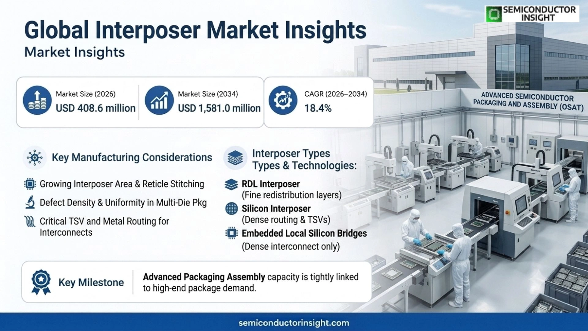
Interposer Market was valued at USD 345.0 million in 2025, is estimated at USD 408.6 million in 2026, and is projected to reach USD 1,581.0 million by 2034, representing a CAGR of 18.4% during 2026–2034. North America is the largest regional market in 2025, while the commercial growth mechanism is increasingly shaped by AI accelerators, HBM integration, chiplet architectures, larger 2.5D packages, advanced substrate routing, and high-density heterogeneous integration.
An interposer is an intermediate routing structure placed between semiconductor dies and the package substrate or between stacked device layers. It redistributes fine-pitch chip connections to a larger pitch, enables die-to-die communication and can incorporate through-silicon vias, redistribution layers, embedded bridges or passive components. Interposers are central to 2.5D and several 3D packaging architectures because they allow logic, memory, RF and other chiplets built on different process nodes to operate as one system.
The market is being reshaped by AI and high-performance computing. Large accelerators need multiple HBM stacks positioned close to logic with thousands of high-speed connections. A 2.5D interposer provides the routing density and electrical performance required to move data between those elements while supporting heterogeneous integration. As accelerator packages grow, interposer area, layer count and power-delivery requirements also increase, raising both technical complexity and value per package.
Interposer competition is no longer limited to one material or architecture. Silicon remains dominant in high-density HPC packages, while RDL interposers and embedded bridges can lower cost or enable larger package dimensions. Glass is gaining attention for dimensional stability, panel-scale processing and RF properties, while organic solutions remain relevant where cost and routing density requirements are less extreme. The winning approach depends on bandwidth, package size, thermal behavior, yield and total system cost.
Segment Analysis: By Type
By type, the market is segmented into 2D Interposer, 2.5D Interposer, and 3D Interposer. The 2.5D category is the leading segment because it provides dense lateral interconnect between chiplets and HBM while maintaining a more mature manufacturing flow than full 3D stacking.
| Type | Technical role | Market position |
|---|---|---|
| 2D Interposer | Primarily redistributes connections or adapts pitch without extensive vertical active-die stacking. Materials can include silicon, glass, ceramic or organic structures depending on electrical and mechanical needs. | Used in lower-complexity packages, sensors, RF modules and applications where routing adaptation is more important than extreme die-to-die bandwidth. |
| 2.5D Interposer | Places multiple active dies side by side on a high-density interposer, often with TSVs or RDL that connect the die to the package substrate. Commonly used to connect logic with HBM. | The leading type. AI accelerators, FPGAs and HPC processors rely heavily on 2.5D integration because it combines high bandwidth, heterogeneous die mixing and production maturity. |
| 3D Interposer | Supports vertical integration and can include active or passive interposer functions, TSVs and dense stacked interfaces. The architecture targets very short interconnects and high integration density. | A high-value emerging segment. Thermal management, test access and yield make full 3D solutions more complex, but advanced memory and chiplet systems create growing demand. |
Why has 2.5D become the preferred architecture for AI accelerators?
AI accelerators need very wide memory interfaces and several HBM stacks positioned close to the compute die. A 2.5D interposer provides thousands of fine-pitch connections while allowing each logic and memory die to be manufactured separately and tested before package assembly. This improves architectural flexibility and can reduce the yield penalty associated with one very large monolithic die. The approach also supports different process nodes for compute, I/O and memory.
Segment Analysis: By Application
By application, the market includes CIS, CPU/GPU, MEMS 3D Capping, RF Devices, Logic SoC, ASIC/FPGA, and High Power LED. ASIC/FPGA is the largest application because custom AI, networking and programmable logic devices increasingly combine compute chiplets and HBM through advanced 2.5D packaging.
| Application | Demand characteristics | |
|---|---|---|
| ASIC/FPGA | Custom accelerators and programmable logic use interposers to connect large logic devices with HBM, I/O chiplets or specialized accelerators. High bandwidth and flexible die partitioning are critical. | The largest application, supported by AI accelerators, networking and data-center systems. |
| CPU/GPU | High-end processors use interposers to combine compute chiplets, cache, HBM and I/O while keeping electrical paths short and power delivery manageable. | A major growth segment as HPC and AI packages become larger and more heterogeneous. |
| CIS | Image-sensor applications can use interposers for wafer-level integration, signal routing and compact camera modules. | A specialized segment where miniaturization and high I/O density matter. |
| MEMS 3D Capping | Glass or silicon interposers can provide hermetic or functional capping, feedthroughs and compact routing for MEMS sensors. | A niche but stable use case in sensors and precision devices. |
| RF Devices | Interposers provide low-loss routing, passive integration and compact module structures for RF front ends and communications devices. | Growing with 5G/6G, radar and compact RF modules. |
| Logic SoC | Chiplet-based SoCs use interposers to separate compute, I/O and accelerator functions while preserving high-bandwidth communication. | An expanding opportunity as monolithic scaling becomes more expensive. |
| High Power LED | Interposers can provide thermal spreading, electrical routing and compact integration in high-brightness LED packages. | A smaller application where thermal and mechanical design are central. |
How does HBM change interposer design requirements?
HBM uses thousands of parallel connections between memory stacks and logic. As more HBM stacks are added, the interposer must provide wider routing, stronger power delivery and larger physical area. TSMC’s CoWoS roadmap toward 5.5-reticle-size interposers reflects this requirement. Larger interposers also increase warpage, defect and yield risk, which is why RDL, embedded bridge and hybrid approaches are being developed alongside full silicon interposers.
Regional Analysis
North America leads the Interposer market by system demand and advanced package design, supported by AI accelerators, FPGAs and high-performance processors. Asia Pacific is the dominant manufacturing region through Taiwan, Japan and South Korea, while Europe retains important RF, MEMS and advanced-packaging research capability.
Why is the interposer market split between design leadership and manufacturing concentration?
Many leading AI and processor architectures are designed by North American companies, but high-volume interposer fabrication and package assembly are concentrated in Asian foundry and OSAT ecosystems. Europe participates through specialized materials, RF, MEMS and advanced packaging R&D. South America and the Middle East remain small direct manufacturing markets and consume interposer technology mainly through imported high-performance systems.
| Region | Position | Growth outlook | Demand profile | What decides supplier selection |
|---|---|---|---|---|
| North America | Largest demand market | Very strong | AI, FPGA, CPU/GPU and data-center design | Bandwidth, HBM integration, package scale and supply assurance |
| Asia Pacific | Manufacturing hub | Very strong | Foundry, OSAT, memory and substrate ecosystem | Yield, capacity, routing density and advanced packaging execution |
| Europe | Specialized technology market | Moderate to strong | RF, MEMS, automotive and R&D | Material performance, reliability and process integration |
| South America | Small direct market | Selective | Imported HPC and electronics systems | Cost and access to packaged semiconductor supply |
| Middle East & Africa | Emerging demand market | Selective | AI infrastructure and telecom systems | Availability and system-level integration |
Competitive Landscape
The market includes TSMC, Murata, Tezzaron, AMD/Xilinx, AGC Electronics, UMC, Plan Optik, Amkor, IMT, ALLVIA, GlobalFoundries, ASE, STATS ChipPAC, SK hynix and Powertech Technology. Competitive advantage depends on routing density, interposer size, TSV yield, material selection and integration with logic and memory.
TSMC has the strongest position in leading-edge AI packaging through CoWoS-S, CoWoS-R and CoWoS-L. The company is scaling interposer area and packaging capacity to support larger AI devices and more HBM. Its advantage is the ability to combine foundry, advanced packaging and test within one turnkey ecosystem.
ASE competes through VIPack, including TSV-based 2.5D/3D integration and FOCoS-Bridge. Amkor and other OSATs offer silicon interposer and advanced packaging services to customers that want foundry-independent backend options. UMC and GlobalFoundries contribute foundry and specialty-process capability.
Material and specialty suppliers such as Murata, AGC, Plan Optik, IMT and ALLVIA compete in glass, RF, MEMS and TSV-related interposer niches. Their opportunities increase where silicon is not the optimal balance of cost, RF loss or panel-scale manufacturability.
| Competitive tier | Representative companies | Commercial basis |
|---|---|---|
| Leading foundry and advanced packaging platforms | TSMC; UMC; GlobalFoundries | Silicon and RDL interposer process integration, wafer fabrication, TSV capability and high-volume packaging ecosystems. |
| OSAT and package integration leaders | ASE Group; Amkor Technology; STATS ChipPAC; Powertech Technology | 2.5D/3D assembly, substrate integration, test and heterogeneous package production. |
| Specialist interposer and material suppliers | Murata; AGC Electronics; Plan Optik AG; Tezzaron Semiconductor; IMT; ALLVIA | Glass, silicon, MEMS, RF and TSV-focused solutions for specialized package architectures. |
Key Market Participants
Murata, Tezzaron Semiconductor, Xilinx (AMD), AGC Electronics, TSMC, UMC, Plan Optik AG, Amkor Technology, IMT, ALLVIA, Inc., GlobalFoundries, ASE Group, STATS ChipPAC, SK hynix, Powertech Technology.
Production Capacity Analysis
Interposer capacity depends on fine-line wafer processing, TSV formation, redistribution layers, wafer thinning, bonding, substrate assembly and advanced package test. Silicon interposers require semiconductor-grade lithography and yield control, while larger AI packages make warpage and defect management more difficult. RDL and bridge technologies create alternate capacity paths.
Silicon interposer manufacturing starts with lithography and dielectric/metal routing on silicon wafers, often combined with TSVs that connect the top routing layer to the package substrate. As interposer area grows beyond normal reticle dimensions, stitching, uniformity and defect density become more important because one defect can affect an expensive multi-die package.
RDL interposers use fine redistribution layers without a full silicon wafer under the entire package. They can reduce cost and support larger dimensions, although routing density and mechanical behavior differ from silicon. Embedded local silicon bridges take the concept further by placing dense silicon only between the chiplets that need it.
Assembly capacity is tightly linked to HBM and high-end package demand. Logic die, memory stacks, interposer, substrate and test must all be available at the same time. This creates a coordinated supply-chain challenge and explains why leading foundries and OSATs are investing heavily in advanced packaging rather than treating it as a low-value backend step.
| Capacity layer | Where it concentrates | Commercial constraint |
|---|---|---|
| Silicon interposer wafer processing | Taiwan, Japan, United States and advanced foundry hubs | TSV yield, fine-line lithography, large-area defect control and wafer thinning. |
| RDL / bridge fabrication | Taiwan, Korea and major OSAT/foundry sites | Line/space capability, panel or wafer size, warpage and integration with substrates. |
| HBM and logic integration | Taiwan, South Korea and advanced packaging clusters | Coordinated supply of logic, HBM, interposer and substrates. |
| Package assembly & test | Taiwan, South Korea, Southeast Asia and global OSAT sites | Thermal control, known-good-die quality, test complexity and package yield. |
Market Dynamics
Interposer demand is accelerating because advanced packaging is becoming a primary method for scaling compute systems. AI and HPC are the strongest drivers, but cost, yield and package complexity create meaningful restraints. The market increasingly rewards architectures that place high-density interconnect only where it provides measurable bandwidth or power benefits.
Market Drivers
| Factor | Directional impact | Why it matters |
|---|---|---|
| AI accelerators and HBM | High | More HBM stacks and larger logic complexes require wider, denser interposer routing. |
| Chiplet architectures | High | Separating functions into smaller dies creates demand for high-bandwidth die-to-die integration. |
| Advanced packaging capacity expansion | High | Foundries and OSATs are adding CoWoS, 2.5D/3D and bridge capacity. |
| 5G, RF and MEMS miniaturization | Medium | Specialty interposers support compact RF, sensor and heterogeneous modules. |
AI moves performance scaling into the package
Transistor scaling alone cannot deliver the memory bandwidth required by large AI models. Interposers place HBM beside compute dies with extremely wide interfaces, making package-level interconnect a performance-critical part of the accelerator. As chiplets and HBM stacks increase, interposer area and complexity grow faster than unit shipments.
Chiplets improve design economics but need dense interconnect
Breaking a large SoC into smaller dies can improve yield and allow each function to use a different process node. The benefit only works if the package provides enough bandwidth and low latency between the dies. Interposers, bridges and fine-pitch RDL provide that physical layer.
Packaging capacity is becoming strategic semiconductor infrastructure
TSMC, ASE and other suppliers are expanding advanced packaging because AI demand has made backend capacity a gating factor for accelerator shipments. Interposer production therefore gains strategic value and attracts capital that historically went mainly to front-end fabs.
Specialty applications broaden material choices
RF, MEMS and photonics applications can favor glass or other interposer materials because of low dielectric loss, dimensional stability or panel-scale processing. These niches create opportunities outside the dominant silicon-HBM architecture.
Market Restraints
| Factor | Directional impact | Why it matters |
|---|---|---|
| High package and interposer cost | High | Large silicon interposers and fine-pitch processes add substantial cost to semiconductor packaging. |
| Yield loss on large interposers | High | Larger area increases defect and warpage risk, especially for reticle-scale and multi-reticle designs. |
| Thermal and mechanical complexity | Medium-High | Logic, HBM and interposer materials expand differently and generate high heat flux. |
| Concentrated advanced-packaging capacity | Medium-High | A limited number of suppliers can support the most advanced high-volume interposer packages. |
Large silicon area is expensive
A full silicon interposer can be much larger than the active logic die, and every additional routing layer or TSV process adds manufacturing steps. For cost-sensitive products, the performance benefit may not justify the package premium, encouraging RDL and bridge alternatives.
Yield becomes more difficult as package area expands
A defect in an interposer can compromise several expensive known-good dies and HBM stacks. Large reticle-spanning interposers therefore require excellent lithography, inspection and process uniformity. Yield improvement is a major economic lever.
Thermal and warpage control become system problems
High-power logic and multiple memory stacks create steep thermal gradients. Different coefficients of thermal expansion across silicon, substrate and molding materials can also cause warpage. Package design must therefore co-optimize electrical, thermal and mechanical performance.
Capacity concentration can constrain product ramps
Advanced interposer and HBM packaging is concentrated among a small number of foundries and OSATs. Strong AI demand can create long lead times or allocation pressure. Customers respond with long-term agreements, multiple packaging architectures and closer co-design with suppliers.
Market Opportunities
Larger CoWoS-class interposers
Next-generation AI accelerators need more HBM and more logic area. Interposers beyond 5x reticle size create opportunities in lithography, RDL, testing and substrate engineering as suppliers scale package dimensions.
RDL and embedded bridges
Local silicon bridges and RDL interposers can lower cost and reduce some large-area silicon constraints. These architectures create new competition and expand advanced packaging into products that cannot justify a full silicon interposer.
Glass interposers
Glass offers attractive dimensional stability, electrical performance and panel-processing potential. If through-glass via and metallization yields improve, glass can address RF, MEMS and selected chiplet applications.
Co-packaged optics
Future AI and networking systems may bring optical engines next to compute die. Interposers can integrate electrical control, photonics and high-speed signaling in one package, opening a new high-value application beyond logic-to-HBM.
Supply Chain Analysis
Interposer Materials & Wafers. Silicon remains dominant for high-density HPC because it uses mature semiconductor processing, while glass and organic materials address lower-loss or lower-cost applications. Material flatness and thermal behavior influence routing yield and package warpage.
TSV / RDL Fabrication. Fine-line lithography, copper plating, dielectric deposition and TSV processing determine signal integrity and usable interconnect density. Larger interposers require strong defect inspection because yield loss scales with area.
Chiplet & HBM Assembly. Known-good logic dies and HBM stacks are bonded onto the interposer using fine-pitch microbumps or hybrid interfaces. Assembly throughput is limited by placement accuracy, thermal budgets and synchronized component availability.
Package & System Integration. The interposer assembly is attached to an organic substrate and combined with heat spreaders or advanced cooling. Final electrical test verifies thousands of high-speed links and power connections before the package enters an AI server, FPGA card or other system.
Recent Developments in the Interposer Market
Developments tracked to September 2026. Entries are dated to the official publication date where available.
- 2026 Capacity
TSMC moved 5.5-reticle-size CoWoS interposers toward volume production after completing certification in 2025. Larger interposers allow more logic and HBM within one package and directly raise routing, power-delivery and yield requirements. Source - 21 April 2026 Technology
TSMC said it is producing 5.5-reticle-size CoWoS and planning even larger versions for AI and HPC. The roadmap confirms that package scaling is becoming a central path to higher compute and memory bandwidth. Source - 19 December 2025 Platform
ASE highlighted VIPack as a vertically integrated advanced packaging platform for AI and data-center systems. The portfolio combines RDL fan-out, TSV-based 2.5D/3D and bridge technologies, giving customers alternatives to full silicon interposers. Source - July 2025 Technology
Intel Foundry published an updated EMIB technology brief covering EMIB-M, EMIB-T and EMIB 3.5D. Embedded silicon bridges provide dense die-to-die connectivity while avoiding the need for a full silicon interposer across the complete package. Source - 28 May 2025 Product
ASE announced FOCoS-Bridge with TSV for next-generation AI and HPC packages. The technology shortens interconnect paths and supports higher I/O density, expanding the competitive set of interposer and bridge architectures. Source
Report Scope & Segmentation
| Attribute | Coverage |
|---|---|
| Report title | Interposer Market, Global Business Strategies 2026-2033 |
| Base / estimate / forecast | 2025 base year; 2026 estimated year; 2034 forecast end year; CAGR measured for 2026–2034. |
| By Type | 2D Interposer; 2.5D Interposer; 3D Interposer |
| By Application | CIS; CPU/GPU; MEMS 3D Capping; RF Devices; Logic SoC; ASIC/FPGA; High Power LED |
| By End User | Semiconductor Manufacturers; Electronics OEMs; Research Institutions |
| By Material Type | Silicon Interposers; Glass Interposers; Organic Interposers |
| Regions | North America, Europe, Asia-Pacific, South America, and Middle East & Africa, with country-level analysis across the principal national markets. |
| Companies | Murata, Tezzaron Semiconductor, Xilinx (AMD), AGC Electronics, TSMC, UMC, Plan Optik AG, Amkor Technology, IMT, ALLVIA, Inc., GlobalFoundries, ASE Group, STATS ChipPAC, SK hynix, Powertech Technology |
| Customization Scope | Free report customization (equivalent to up to 4 analyst working days) with purchase. Addition or alteration to country, regional and segment scope. |
Frequently Asked Questions
What is the size of the Interposer market?
The global Interposer market is valued at USD 345.0 million in 2025, is estimated at USD 408.6 million in 2026, and is projected to reach USD 1,581.0 million by 2034, representing an 18.4% CAGR during 2026–2034.
Which region leads the Interposer market?
North America is the largest demand market because major AI accelerator, FPGA and processor designers are concentrated in the region, while Taiwan and broader Asia Pacific form the core high-volume manufacturing and advanced-packaging ecosystem.
Which interposer type is largest?
2.5D interposers are the leading type because they provide high-density lateral connections between logic chiplets and HBM while using a more mature manufacturing flow than full 3D stacking.
Which application leads interposer demand?
ASIC/FPGA is the largest application, supported by AI accelerators, networking devices and programmable logic that use interposers to connect high-performance logic with HBM and other chiplets.
Why are interposers important for AI chips?
AI accelerators need very wide memory interfaces and several HBM stacks. An interposer creates thousands of short, high-speed connections between logic and memory, delivering more bandwidth and lower energy per bit than routing those signals through a conventional package substrate alone.
What materials are used for interposers?
The main materials are silicon, glass and organic/RDL structures. Silicon leads in high-density HPC, glass offers attractive dimensional and RF properties, and RDL or organic approaches can reduce cost and support larger package dimensions.
What are the main restraints on interposer adoption?
The principal restraints are high cost, large-area yield loss, thermal and warpage complexity, and concentrated advanced-packaging capacity. These issues become more important as AI packages expand beyond several reticle sizes.
Who are the major Interposer companies?
Major companies include TSMC, Murata, Tezzaron Semiconductor, AMD/Xilinx, AGC Electronics, UMC, Plan Optik, Amkor, IMT, ALLVIA, GlobalFoundries, ASE, STATS ChipPAC, SK hynix and Powertech Technology.
How are bridge technologies different from full interposers?
Embedded bridges place dense silicon only between chiplets that need very high bandwidth. This can reduce silicon area and simplify some routing compared with a full interposer while preserving fine-pitch connectivity at critical die boundaries.
Where are the strongest future opportunities?
The strongest opportunities are in larger AI interposers, RDL and embedded bridges, glass interposers and co-packaged optics. All four areas address the need for more bandwidth, larger package scale or lower cost in heterogeneous semiconductor systems.
Research Sources & Evidence Base

Get Sample Report PDF for Exclusive Insights
Report Sample Includes
- Table of Contents
- List of Tables & Figures
- Charts, Research Methodology, and more...
 Download Sample Report PDF


