
Laser Annealing (LSA, DSA) Equipment Market Insights
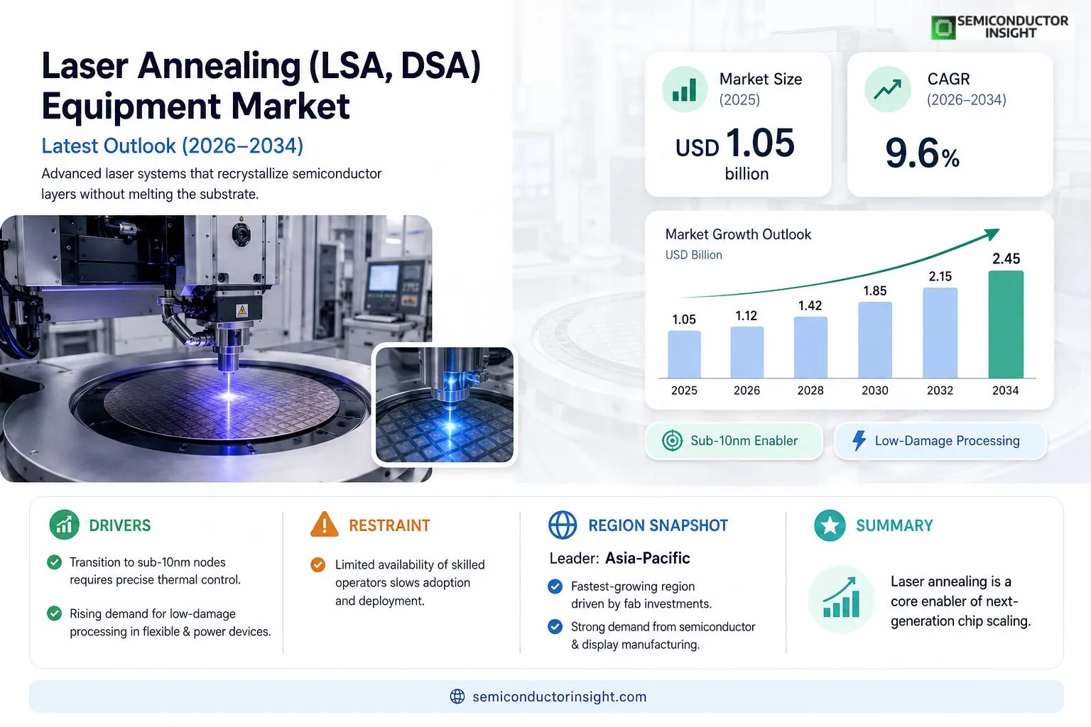
Global Laser Annealing (LSA, DSA) Equipment market size was valued at USD 1.05 billion in 2025. The market is projected to grow from USD 1.12 billion in 2026 to USD 2.45 billion by 2034, exhibiting a CAGR of 9.6% during the forecast period.
Laser annealing equipment utilizes short‑pulse lasers to recrystallize amorphous silicon or other semiconductor layers without melting the substrate, enabling precise dopant activation and defect reduction for advanced logic and memory devices. The technology supports both line‑scan (LSA) and direct‑write (DSA) processes, offering superior thermal budget control compared with conventional furnace annealing.The market is accelerating because semiconductor manufacturers are shifting toward sub‑10 nm nodes where thermal management is critical, while emerging applications such as flexible electronics and power devices demand low‑damage processing. Moreover, increasing capital expenditures by leading fabs,such as Applied Materials, Tokyo Electron and ASML,are driving adoption of high‑throughput laser annealers. Collaborative R&D programs between equipment vendors and chipmakers further reinforce growth momentum.
MARKET DRIVERS
Technological Advancements in Semiconductor Processing
Laser Annealing (LSA, DSA) Equipment Market is being propelled by rapid improvements in laser pulse control and beam uniformity, which enable finer line widths and higher throughput for advanced node manufacturing. These innovations reduce defect rates and improve yield, making laser annealing a preferred choice over conventional thermal methods.
Growing Demand for Advanced Packaging
Advanced packaging formats such as fan-out wafer-level packaging (FOWLP) and heterogeneous integration rely heavily on precise annealing steps. The ability of laser systems to deliver localized heating without damaging surrounding structures is a key driver for adoption across leading foundries.
➤ “Laser annealing delivers up to 30 % faster cycle times while maintaining critical dimension control, positioning it as a strategic enabler for next‑generation chips.”
Overall, the convergence of high‑volume manufacturing needs and the push toward sub‑10 nm node technologies creates a robust growth environment for Laser Annealing (LSA, DSA) Equipment Market.
MARKET CHALLENGES
High Capital Expenditure
Investing in state‑of‑the‑art laser annealing platforms requires a substantial upfront outlay, which can deter smaller fab operators. The total cost of ownership, including maintenance and specialized consumables, remains a critical barrier for broader market penetration.
Other Challenges
Process Integration Complexity
Integrating laser annealing into existing process flows demands careful thermal budgeting and precise alignment, often requiring extensive engineering support and validation cycles.
MARKET RESTRAINTS
Limited Availability of Skilled Operators
The specialized knowledge required to operate and maintain high‑precision laser systems constrains rapid adoption. Training programs are still emerging, and the scarcity of experienced technicians can slow deployment timelines for Laser Annealing (LSA, DSA) Equipment Market.
MARKET OPPORTUNITIES
Expansion into Emerging Materials
New material systems such as high‑k dielectrics and two‑dimensional (2D) semiconductors present untapped applications for laser annealing. Tailoring laser parameters to these substrates can unlock novel device architectures, offering a significant growth avenue for Laser Annealing (LSA, DSA) Equipment Market.
Laser Annealing (LSA, DSA) Equipment Market Trends
Shift to Sub‑10 nm Nodes Drives Adoption
Laser Annealing (LSA, DSA) Equipment Market is experiencing accelerated uptake as semiconductor manufacturers target sub‑10 nm process nodes. At these dimensions, conventional furnace annealing cannot provide the required thermal budget control without compromising device integrity. Short‑pulse laser annealers deliver localized heating that recrystallizes semiconductor layers while preserving the underlying substrate, thereby supporting tighter pitch and higher transistor density. This capability has become a decisive factor for leading fabs seeking to maintain yield while scaling beyond the 10 nm threshold.
Other Trends
Flexible Electronics and Power Device Expansion
Emerging application domains such as flexible displays, wearable sensors, and wide‑bandgap power devices are creating new demand for low‑damage processing. Laser annealing technology enables defect‑reduced activation of dopants on thin, bendable substrates where thermal shock must be minimized. As manufacturers diversify their product portfolios, equipment providers are integrating line‑scan (LSA) and direct‑write (DSA) capabilities to address the varied geometry and throughput requirements of these novel markets.
Capital Investment and Collaborative R&D Strengthen Growth
Major semiconductor equipment vendors,including Applied Materials, Tokyo Electron, and ASML,are allocating substantial capital expenditures to expand their laser annealing product lines. These investments are complemented by joint research programs that pair vendor expertise with chipmaker process engineers. Collaborative development accelerates the introduction of high‑throughput laser systems, improves tool reliability, and shortens the qualification cycle for new device architectures. The combined effect of financial commitment and shared innovation is solidifying Laser Annealing (LSA, DSA) Equipment Market’s position as a core enabler of next‑generation semiconductor manufacturing.
COMPETITIVE LANDSCAPEKey Industry Players
Laser Annealing (LSA, DSA) Equipment Market Competitive Overview
The Laser Annealing (LSA, DSA) equipment segment is dominated by a handful of global fabs equipment leaders whose extensive R&D spend and deep customer relationships shape market structure. Applied Materials, Tokyo Electron and ASML collectively account for more than half of the market revenue, leveraging high‑throughput line‑scan systems and integrated process suites that align with sub‑10 nm node roadmaps. Their platforms are favored by leading semiconductor manufacturers for precise dopant activation, low thermal budget, and scalability across wafer sizes up to 300 mm. These incumbents benefit from long‑term supply contracts and co‑development programs that reinforce barriers to entry, while their financial strength supports rapid technology refresh cycles that sustain the market’s 9.6 % CAGR projection through 2034.Beyond the top tier, a diverse set of niche and emerging players contributes specialized capabilities and regional reach. Companies such as nLIGHT, Coherent, Lumentum and IPG Photonics offer ultrafast fiber and solid‑state lasers tailored for direct‑write (DSA) processes, addressing flexible electronics and power device markets. Spectra‑Physics (now part of MKS Instruments) and NovaLases provide compact, high‑precision systems for research and pilot lines. Asian manufacturers,including NAURA Technology Group, Shanghai Electric and Fujitsu,are expanding their portfolios to capture growing domestic fab investments, while firms like SPTS Technologies and Trion Technologies focus on cost‑effective solutions for smaller fabs. This layered ecosystem enhances competition, drives innovation, and creates opportunities for strategic collaborations across the laser annealing value chain.
List of Key Laser Annealing Equipment Companies Profiled
- Applied Materials, Inc.
- Tokyo Electron Ltd.
- ASML Holding N.V.
- nLIGHT, Inc.
- Coherent, Inc.
- Lumentum Holdings Inc.
- IPG Photonics Corporation
- Spectra-Physics (MKS Instruments)
- NovaLases Technology Co., Ltd.
- Fujitsu Limited
- SPTS Technologies, Inc.
- NAURA Technology Group Co., Ltd.
- Shanghai Electric Group Co., Ltd.
- Trion Technologies, Inc.
- Oxide Semiconductor Equipment Co.
Segment Analysis:
| Segment Category | Sub-Segments | Key Insights |
| By Type |
|
Line‑Scan Laser Annealing
|
| By Application |
|
Advanced Logic Devices
|
| By End User |
|
Foundries
|
| By Integration Mode |
|
In‑line Integration with Lithography
|
| By Process Scale |
|
High‑Volume Production
|
Regional Analysis: North America
United States
The semiconductor sector in the US is a primary driver for laser annealing equipment, particularly for wafer processing and microchip fabrication. Demand here is linked to advancements in chip design and the increasing complexity of integrated circuits. Companies are seeking LSA/DSA solutions that enhance performance and reliability.
The US microelectronics market is witnessing significant innovation in areas like flexible electronics and advanced packaging. This fuels the need for specialized laser annealing equipment capable of handling diverse materials and intricate designs within those applications.
The manufacturing of high-precision components, including those used in aerospace and automotive industries, benefits from laser annealing’s ability to improve material properties like hardness and wear resistance. This creates opportunities for suppliers specializing in customized laser annealing solutions.
Ongoing R&D efforts in the US are focused on developing more energy-efficient laser annealing systems and exploring novel applications for the technology. This includes research into advanced laser sources and process control techniques to enhance accuracy and minimize waste.
Europe
Europe represents a significant market for Laser Annealing (LSA, DSA) Equipment, with key countries like Germany, France, and the UK driving adoption. The region’s strong emphasis on sustainable manufacturing processes and advanced materials contributes to the demand for efficient and precise laser annealing technologies. European businesses are increasingly focusing on utilizing laser annealing for applications in the automotive, aerospace, and renewable energy sectors. The market is characterized by stringent quality standards and a growing interest in environmentally friendly solutions. Business strategies prioritize developing systems that align with Europe’s commitment to circular economy principles.
Asia-Pacific
Asia-Pacific is emerging as the fastest-growing region for Laser Annealing (LSA, DSA) Equipment Market. Driven by rapid industrialization in countries like China, Japan, and South Korea, the demand for laser annealing is surging across various industries. Semiconductor manufacturing, display panel production, and the fabrication of electronic components are key application areas. Government initiatives supporting technological advancements and manufacturing competitiveness are further fueling market growth. Companies in this region are actively seeking advanced laser annealing systems to improve product quality, increase production efficiency, and enhance their overall competitiveness.
South America
South America presents a moderate growth opportunity for Laser Annealing (LSA, DSA) Equipment. Countries like Brazil and Argentina are seeing increasing investments in manufacturing and technology sectors, leading to a gradual rise in demand for laser annealing technologies. The primary applications in this region are focused on automotive components, metal fabrication, and the production of consumer electronics. Challenges include infrastructure limitations and economic uncertainties, but the long-term potential remains promising as industrialization progresses.
Middle East & Africa
The Middle East and Africa represent a developing market for Laser Annealing (LSA, DSA) Equipment. Driven by investments in infrastructure development, automotive manufacturing, and aerospace industries, the demand is expected to increase steadily. Key applications include precision metal components, automotive parts, and components for the oil and gas sector. The market is characterized by a growing need for advanced manufacturing solutions to enhance efficiency and product quality, leading to opportunities for laser annealing technology providers.
Report Scope
This market research report provides a comprehensive analysis of the Laser Annealing (LSA, DSA) Equipment Market , covering the forecast period 2026–2034. It offers detailed insights into market dynamics, technological advancements, competitive landscape, and key trends shaping the industry.
Key focus areas of the report include:
- Market Overview: The report begins with an overview outlining its current market scenario, key growth indicators, and industry transformation drivers. It discusses macroeconomic factors, demand–supply balance, regulatory landscape, and the strategic role of semiconductors in powering advancements across industries such as automotive, telecommunications, consumer electronics, and industrial automation.
- Market Size & Forecast: Historical data and future projections for revenue, unit shipments, and market value across major regions and segments.
- Segmentation Analysis: Detailed breakdown by product type, technology, application, and end-user industry to identify high-growth segments and investment opportunities.
- Regional Insights: Insights into market performance across North America, Europe, Asia-Pacific, Latin America, and the Middle East & Africa, including country-level analysis where relevant.
- Competitive Landscape: Profiles of leading market participants, including their product offerings, R&D focus, manufacturing capacity, pricing strategies, and recent developments such as mergers, acquisitions, and partnerships.
- Technology Trends & Innovation: Assessment of emerging technologies, integration of AI/IoT, semiconductor design trends, fabrication techniques, and evolving industry standards.
- Market Drivers & Restraints: Evaluation of factors driving market growth along with challenges, supply chain constraints, regulatory issues, and market-entry barriers.
- Stakeholder Insights: Insights for component suppliers, OEMs, system integrators, investors, and policymakers regarding the evolving ecosystem and strategic opportunities.
Primary and secondary research methods are employed, including interviews with industry experts, data from verified sources, and real-time market intelligence to ensure the accuracy and reliability of the insights presented.
FREQUENTLY ASKED QUESTIONS:
What is the current market size of Laser Annealing (LSA, DSA) Equipment Market?
-> Laser Annealing (LSA, DSA) Equipment Market was valued at USD 1.05 billion in 2025 and is expected to reach USD 2.45 billion by 2034.
Which key companies operate in Laser Annealing (LSA, DSA) Equipment Market?
-> Key players include Applied Materials, Tokyo Electron, and ASML, among others.
What are the key growth drivers?
-> Key growth drivers include transition to sub‑10 nm nodes, demand for low‑damage processing in flexible electronics and power devices, and rising capital expenditures by leading fabs.
Which region dominates the market?
-> Asia‑Pacific is the fastest‑growing region, while Europe remains a significant market.
What are the emerging trends?
-> Emerging trends include integration of laser annealing in flexible electronics, power device manufacturing, and collaborative R&D programs between equipment vendors and semiconductor manufacturers.

Get Sample Report PDF for Exclusive Insights
Report Sample Includes
- Table of Contents
- List of Tables & Figures
- Charts, Research Methodology, and more...
 Download Sample Report PDF

