
Key Statistics
Key Takeaways
- 3D Through-Silicon Via (TSV) is the leading type because the published report identifies 3D TSV as the dominant technology for high-density vertical integration and it remains a foundational route for connecting logic, memory and interposers.
- Monolithic 3D IC is the strongest technology-growth theme as hybrid bonding, sub-10-micron pitches and direct die stacking are reducing interconnect distance and opening denser vertical architectures that move beyond conventional micro-bump scaling.
- Consumer Electronics remains the principal application, where smartphones, wearables and gaming devices reward smaller package area and lower power, making vertical integration commercially attractive when more functionality must fit within fixed mechanical envelopes.
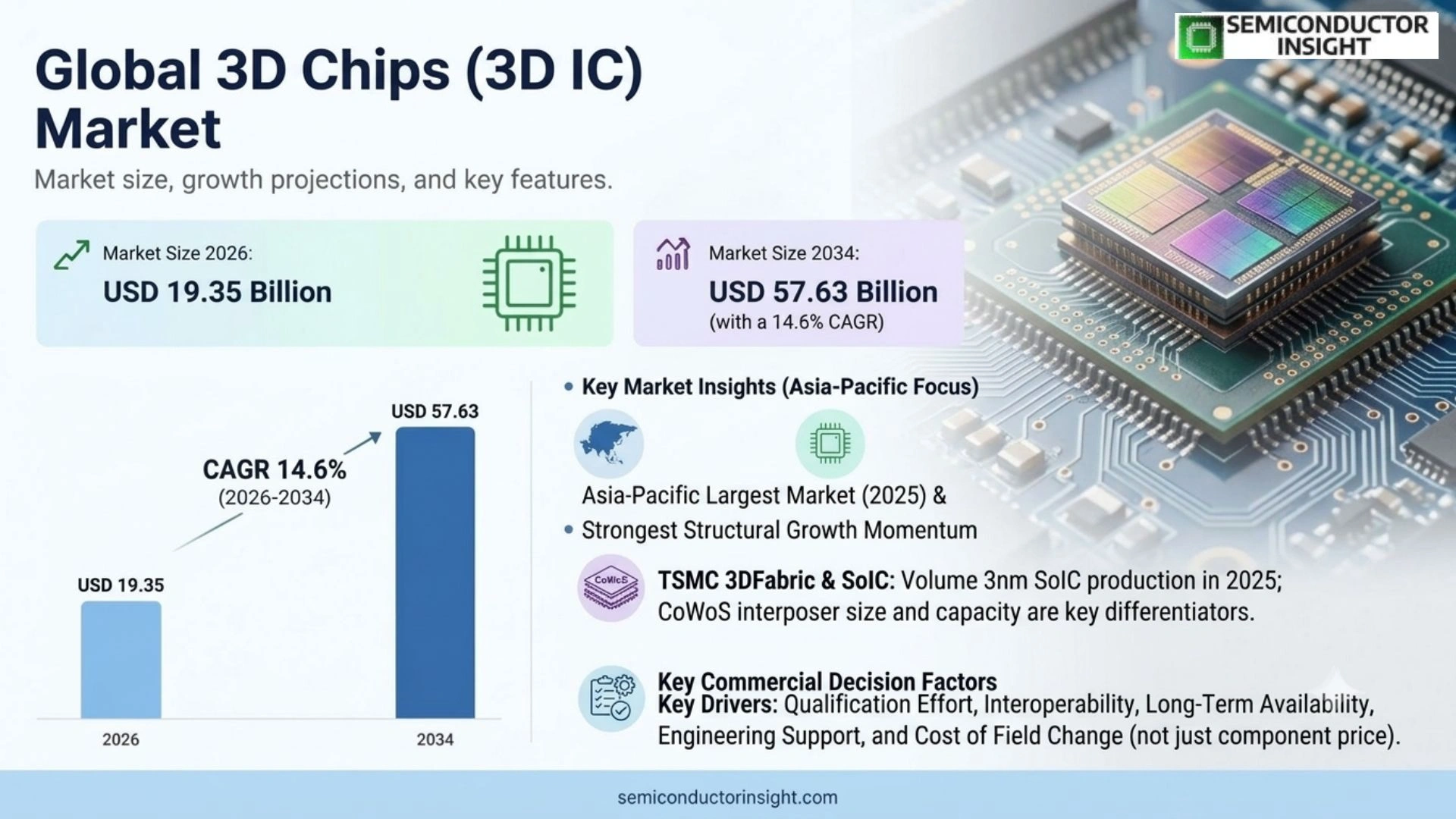
- Asia Pacific is the largest regional market in 2025, supported by TSMC, Samsung, ASE and major memory manufacturers concentrate advanced packaging, foundry and high-bandwidth-memory capabilities across Taiwan, South Korea, Japan and China, while the report FAQ states the region represents more than 60% of global production.
- Asia Pacific has the strongest regional growth profile because the region combines the largest existing advanced-packaging base with continued investment in CoWoS, SoIC, HBM integration, hybrid bonding and domestic semiconductor capacity.
- thermal, yield and capital-intensity constraints is the main structural restraint, slowing qualification, capacity conversion or supplier switching.
3D Chips (3D IC) Market Overview
3d Chips (3d ic) was valued at USD 16.88 billion in 2025 and is projected to reach USD 57.63 billion by 2034, representing a 14.6% CAGR during 2026–2034. The 2026 estimated market size is USD 19.35 billion. Asia Pacific is the largest market in 2025, while Asia Pacific shows the strongest structural growth momentum.
3D chips or 3D integrated circuits vertically integrate multiple active or passive dies using technologies such as through-silicon vias, micro-bumps, hybrid bonding and wafer-level stacking. The published scope includes 3D WLCSP, 3D TSV, monolithic 3D IC and 2.5D interposer approaches, reflecting a market that spans true vertical stacking and closely related heterogeneous-integration architectures used to overcome monolithic scaling limits.
The commercial architecture begins with known-good dies manufactured on one or more process nodes, followed by wafer thinning, bonding, TSV or direct copper interconnect, redistribution layers, underfill or encapsulation, and system-level test. Modern 3D integration can place logic directly over an active base die or connect compute chiplets with HBM, reducing interconnect distance while increasing bandwidth density and enabling designers to mix process technologies inside one package.
Demand grows when system architects can no longer meet compute, memory-bandwidth, area or power targets with a single monolithic die. AI accelerators, server processors and advanced mobile chips increasingly divide functionality into chiplets and reconnect them through 2.5D or 3D packaging. That shifts value from transistor scaling alone toward package co-design, bonding precision, known-good-die test and thermal engineering.
Segment Analysis: By Type
By type, the 3d chips (3d ic) is segmented into 3D Wafer-Level Chip-Scale Packaging (WLCSP), 3D Through-Silicon Via (TSV), Monolithic 3D IC, 2.5D Interposer Technology, Others. 3D Through-Silicon Via (TSV) is the leading segment, while Monolithic 3D IC has the strongest growth momentum. The distinction reflects different performance, integration, manufacturing and qualification requirements across the published scope. In 3d chips (3d ic), commercial decisions also depend on qualification effort, interoperability, long-term availability, engineering support and the cost of a field change after deployment. Suppliers that reduce those risks can protect design wins across multiple system generations, whereas vendors competing only on component price face a more difficult path into applications where revalidation or architecture changes create meaningful cost for the customer.
| Type | Technical / purchasing role | Market position |
|---|---|---|
| 3D Wafer-Level Chip-Scale Packaging (WLCSP) | WLCSP stacks or integrates dies at wafer scale to reduce package footprint and interconnect length, making the approach useful where miniaturization and high manufacturing throughput are priorities. The technology can support mobile, sensor and memory-oriented products but requires precise wafer handling, thinning, alignment and yield control across a large processed area. | Established high-volume route. Its strength is compact form factor and wafer-level economics, while the most demanding AI and HPC packages increasingly combine WLCSP concepts with more complex interposer, HBM and hybrid-bonding architectures. |
| 3D Through-Silicon Via (TSV) | TSVs create vertical electrical connections through silicon, enabling stacked memory, logic-memory integration and high-density 2.5D or 3D packages. The published report identifies this as the dominant type, and the technology remains central to HBM stacks and many advanced packaging flows where bandwidth density must exceed what package traces can deliver. | Largest technology segment. TSV capability is deeply embedded in advanced memory and heterogeneous integration, although suppliers continue reducing pitch and combining TSVs with finer bonding approaches to improve power, density and thermal behavior. |
| Monolithic 3D IC | Monolithic 3D techniques build or bond active device layers with extremely fine vertical connections, targeting much denser interconnect than conventional package-level stacking. Hybrid bonding and direct copper interfaces reduce parasitics and can improve bandwidth per watt, but process integration, alignment, thermal limits and yield remain demanding. | Strongest technology-growth theme. TSMC SoIC and Intel Foveros Direct demonstrate the shift toward sub-10-micron and direct-bond architectures, with UCIe 2.0 and 3.0 adding a standards framework for increasingly dense chiplet systems. |
| 2.5D Interposer Technology | 2.5D systems place multiple dies side by side on silicon, organic or redistribution-layer interposers, providing dense routing between logic chiplets and HBM without stacking every active die vertically. The approach is widely used in AI accelerators and networking because it balances integration density with more manageable thermal and assembly risk. | Large adjacent segment and bridge to full 3D. CoWoS, EMIB and similar platforms remain essential for scaling package size, HBM count and chiplet reuse while hybrid-bonding 3D stacks develop further. |
| Others | Other approaches include fan-out, bridge, panel-level and application-specific heterogeneous-integration technologies that combine logic, memory, RF, photonics or passive components. Their commercial role depends on the package architecture, cost target and available assembly ecosystem rather than a single universal process. | Fragmented opportunity. Innovation is strong because designers increasingly choose the package stack around workload requirements instead of forcing every function onto one process node. |
Manufacturing process and end-user structure
The source page further segments the market by die-to-die, wafer-to-wafer and chip-to-wafer bonding, and by foundries, IDMs, fabless semiconductor companies and OSAT providers. This structure matters because each participant captures different value: foundries optimize front-end and wafer-level integration, OSATs scale assembly and test, while fabless companies increasingly co-design chiplets, memory interfaces and packages as one system. In 3d chips (3d ic), commercial decisions also depend on qualification effort, interoperability, long-term availability, engineering support and the cost of a field change after deployment. Suppliers that reduce those risks can protect design wins across multiple system generations, whereas vendors competing only on component price face a more difficult path into applications where revalidation or architecture changes create meaningful cost for the customer.
Segment Analysis: By Application
By application, the market is segmented into Consumer Electronics, Telecommunications, Automotive Electronics, Industrial Applications, Others. Consumer Electronics represents the most important demand pool, while Automotive Electronics has the strongest structural momentum as customers adopt new architectures and raise performance, reliability or manufacturing requirements. In 3d chips (3d ic), commercial decisions also depend on qualification effort, interoperability, long-term availability, engineering support and the cost of a field change after deployment. Suppliers that reduce those risks can protect design wins across multiple system generations, whereas vendors competing only on component price face a more difficult path into applications where revalidation or architecture changes create meaningful cost for the customer.
| Application | Demand characteristics |
|---|---|
| Consumer Electronics | The report identifies consumer electronics as the leading application. Smartphones and wearables use advanced packaging to increase functionality within strict thickness and battery constraints, while gaming and premium devices benefit from tighter CPU, GPU, memory and RF integration. High volumes reward wafer-level processes that can achieve repeatable yield and cost across millions of units. |
| Telecommunications | Routers, switches, base stations and optical-networking systems increasingly use chiplets and advanced packages to combine high-speed SerDes, packet processing and memory. 2.5D and 3D integration helps manage reticle limits while increasing bandwidth density, which is valuable as Ethernet and telecom interfaces migrate toward 800G, 1.6T and future higher-rate architectures. |
| Automotive Electronics | ADAS and centralized vehicle compute require more processing and memory bandwidth without unlimited board area or power. 3D integration can combine compute, memory and specialized accelerators in compact packages, but automotive qualification makes thermal cycling, interconnect reliability and long product support critical before higher-density packages can move into volume vehicle platforms. |
| Industrial Applications | Robotics, machine vision, edge AI and industrial control can benefit from heterogeneous integration when a compact module must combine compute, memory, sensor processing and connectivity. Adoption is slower than in data centers because product lifecycles are longer, but the ability to reuse chiplets across multiple equipment families can improve development economics. |
| Others | AI accelerators, HPC processors, defense, medical, photonics and specialized computing form a high-value group outside the named mainstream applications. These programs often adopt advanced packaging first because system performance or form factor justifies higher assembly cost and because chiplet reuse can reduce the expense of building one very large leading-edge monolithic die. |
Regional Analysis
Asia Pacific leads the 3d chips (3d ic) in 2025, while Asia Pacific has the strongest growth outlook. Regional demand differs because manufacturing concentration, infrastructure investment, standards adoption, local engineering ecosystems and customer qualification practices vary materially by geography. In 3d chips (3d ic), commercial decisions also depend on qualification effort, interoperability, long-term availability, engineering support and the cost of a field change after deployment. Suppliers that reduce those risks can protect design wins across multiple system generations, whereas vendors competing only on component price face a more difficult path into applications where revalidation or architecture changes create meaningful cost for the customer.
How does regional demand differ across the 3d chips (3d ic)?
Asia Pacific is treated as the largest region because the production ecosystem for advanced foundry, memory and packaging is concentrated in Taiwan, South Korea, Japan and China. The client page contains a contradiction: one regional paragraph says North America dominates, while the FAQ says Asia Pacific dominates with more than 60% of global production. The overview uses Asia Pacific as the defensible largest-market position and records the conflict in reviewer notes.
| Region | Position | Growth outlook | Demand profile | What decides supplier selection |
|---|---|---|---|---|
| Asia Pacific | Largest | Highest | Foundry, memory and advanced-packaging led | Capacity, yield, HBM integration, hybrid bonding and ecosystem proximity |
| North America | Major technology market | Strong | AI/HPC design and domestic packaging investment | Leading architectures, CHIPS-backed capacity, ecosystem and trusted supply |
| Europe | Strategic developing market | Strengthening | Automotive, research and packaging investment | Pilot-line access, packaging capability, automotive reliability and regional resilience |
| South America | Nascent | Selective | Imported advanced electronics and limited local integration | Cost, access to global packaging partners and system demand |
| Middle East & Africa | Early stage | Selective | AI infrastructure and technology diversification | Capital access, partner ecosystem and imported advanced packaging |
Competitive Landscape
Competition spans foundries, IDMs, memory manufacturers and OSATs because 3D integration is a system capability rather than a single component. TSMC, Samsung and Intel compete with proprietary packaging platforms, while ASE, Amkor and JCET scale outsourced assembly and test. Memory suppliers such as Micron participate through HBM and stacked-memory products that are tightly coupled to the package architecture.
TSMC’s 3DFabric portfolio combines SoIC 3D stacking with CoWoS interposer packaging, giving customers a route from dense logic-on-logic bonding to large logic-plus-HBM systems. The company states that 3nm SoIC stacking entered volume production in 2025 and that CoWoS interposer sizes continue increasing, making capacity and ecosystem access important competitive differentiators for AI customers. In 3d chips (3d ic), commercial decisions also depend on qualification effort, interoperability, long-term availability, engineering support and the cost of a field change after deployment. Suppliers that reduce those risks can protect design wins across multiple system generations, whereas vendors competing only on component price face a more difficult path into applications where revalidation or architecture changes create meaningful cost for the customer.
Intel and Samsung emphasize vertically integrated foundry-plus-packaging strategies. Intel’s Foveros Direct 3D uses hybrid bonding and can be combined with EMIB, while Samsung’s advanced package platform includes I-Cube and 3D packaging formerly known as X-Cube. Their competitive advantage comes from co-optimizing silicon, package and system architecture under one technology roadmap. In 3d chips (3d ic), commercial decisions also depend on qualification effort, interoperability, long-term availability, engineering support and the cost of a field change after deployment. Suppliers that reduce those risks can protect design wins across multiple system generations, whereas vendors competing only on component price face a more difficult path into applications where revalidation or architecture changes create meaningful cost for the customer.
OSATs such as ASE and Amkor compete by scaling multi-die assembly, test and heterogeneous integration for customers that do not own packaging factories. ASE’s VIPack portfolio includes TSV-based 2.5D/3D IC and fan-out technologies, while Amkor’s U.S. investment demonstrates how packaging capacity itself has become strategically important for supply resilience and AI growth. In 3d chips (3d ic), commercial decisions also depend on qualification effort, interoperability, long-term availability, engineering support and the cost of a field change after deployment. Suppliers that reduce those risks can protect design wins across multiple system generations, whereas vendors competing only on component price face a more difficult path into applications where revalidation or architecture changes create meaningful cost for the customer.
Tier structure
| Competitive tier | Representative participants | How suppliers compete |
|---|---|---|
| Integrated foundry/platform leaders | TSMC; Samsung Electronics; Intel | Compete through proprietary 2.5D/3D platforms, leading wafer technology, hybrid bonding, co-design ecosystems and large-scale capacity. |
| Global OSAT & packaging leaders | ASE Group; Amkor Technology; JCET | Compete on assembly yield, HBM integration, fan-out, TSV, bridge and test capability for multi-die systems across many customers. |
| Memory & system participants | Micron Technology; Broadcom; STMicroelectronics | Create demand and differentiation through HBM, networking, automotive and application-specific systems that require advanced integration. |
Key companies profiled
Companies profiled in the report include Taiwan Semiconductor Manufacturing Company Limited (TSMC); Samsung Electronics Co., Ltd.; Intel Corporation; ASE Group; Amkor Technology; Micron Technology; Broadcom Inc.; STMicroelectronics N.V.; Jiangsu Changjiang Electronics Technology. Competitive position varies by technical domain and customer qualification depth. Scale supports global availability, while specialist suppliers can retain strong positions where standards knowledge, process integration, low-power design, materials expertise or field support are more important than component price alone.
Production Capacity Analysis
Production capacity is the central constraint in 3D IC commercialization because advanced packages require specialized wafer bonding, thinning, TSV, interposer, substrate, HBM and test infrastructure. Capacity is especially tight when AI accelerators need very large interposers and multiple HBM stacks. The market therefore depends on coordinated expansion across foundries, memory suppliers, OSATs and materials vendors rather than a single wafer-fab bottleneck.
Asia Pacific holds the deepest installed base. TSMC, Samsung, ASE, memory manufacturers and many substrate or equipment suppliers are located close together, reducing logistics and engineering friction during package ramp. TSMC’s 2025 annual-report disclosure that 3nm SoIC stacking entered volume production and that larger CoWoS variants are scaling in 2026 illustrates how the region converts process development into high-volume capacity.
North America is expanding from a smaller advanced-packaging manufacturing base. CHIPS awards to Amkor, SK hynix and GlobalFoundries support packaging, HBM and hybrid-bonding capability in Arizona, Indiana and New York. These projects matter because AI chips produced domestically still require advanced assembly and test before becoming deployable systems, and packaging capacity can determine how much value remains in-region.
Yield is a system property in 3D integration. Known-good-die screening, bond alignment, wafer warpage, micro-bump or copper interface quality, TSV integrity and thermal behavior all interact. As more dies are assembled into one package, the economic cost of a defect rises, so test insertion and repair strategy become essential parts of capacity planning rather than simple back-end inspection.
3D Chips (3D IC) Market Dynamics: Drivers, Restraints and Opportunities
3D integration is moving from a specialized packaging technique into a mainstream route for scaling AI, HPC and memory systems beyond monolithic reticle and bandwidth limits. Growth is strong because chiplets can mix process nodes and HBM, but the market is constrained by heat, yield, advanced-packaging capacity and co-design complexity. Standards such as UCIe are reducing interoperability risk while foundries and OSATs expand production.
MARKET DRIVERS
Drivers Impact Analysis*
| Factor | Relative impact* | Commercial mechanism |
|---|---|---|
| AI & HPC bandwidth demand | High | Logic-HBM integration and large multi-die packages are becoming essential to accelerator performance. |
| Chiplet economics | High | Smaller dies can improve yield and enable node mixing compared with one very large monolithic die. |
| Hybrid bonding & fine-pitch interconnect | Medium-High | Denser vertical links improve bandwidth density and energy efficiency. |
| Advanced-packaging investment | Medium-High | New capacity expands the number of customers able to adopt 3D architectures in volume. |
AI accelerators require logic and HBM to function as one system
Training and inference processors consume enormous memory bandwidth. 2.5D and 3D packages place logic close to multiple HBM stacks, reducing interconnect distance and increasing bandwidth density beyond what a conventional PCB interface can deliver. This makes advanced packaging part of the compute architecture itself and directly ties 3D IC demand to AI infrastructure spending. In 3d chips (3d ic), commercial decisions also depend on qualification effort, interoperability, long-term availability, engineering support and the cost of a field change after deployment. Suppliers that reduce those risks can protect design wins across multiple system generations, whereas vendors competing only on component price face a more difficult path into applications where revalidation or architecture changes create meaningful cost for the customer.
Chiplets improve design reuse and reticle economics
Dividing a large SoC into smaller chiplets allows each function to use the process node that best fits cost and performance. Designers can reuse I/O, cache or accelerator tiles across product families and avoid putting every block on the newest node. Advanced packaging then reconnects the pieces, converting package technology into a tool for both yield management and portfolio economics.
Hybrid bonding raises vertical interconnect density
TSMC SoIC, Intel Foveros Direct and UCIe 2.0 all point toward much finer die-to-die connections. Direct copper or very fine-pitch bonding reduces parasitic resistance and capacitance and can lower the energy required to move data between stacked dies. Those gains make true 3D architectures more attractive for bandwidth-limited systems. In 3d chips (3d ic), commercial decisions also depend on qualification effort, interoperability, long-term availability, engineering support and the cost of a field change after deployment. Suppliers that reduce those risks can protect design wins across multiple system generations, whereas vendors competing only on component price face a more difficult path into applications where revalidation or architecture changes create meaningful cost for the customer.
Public investment expands advanced-packaging capacity
U.S. CHIPS awards and European Chips Act programs explicitly support advanced packaging, assembly and test. The policy focus reflects a strategic realization that leading wafer capacity alone is insufficient if high-value chips must still travel overseas for HBM integration or chiplet assembly. New regional capacity broadens the supplier base and can accelerate customer adoption. In 3d chips (3d ic), commercial decisions also depend on qualification effort, interoperability, long-term availability, engineering support and the cost of a field change after deployment. Suppliers that reduce those risks can protect design wins across multiple system generations, whereas vendors competing only on component price face a more difficult path into applications where revalidation or architecture changes create meaningful cost for the customer.
MARKET RESTRAINTS
Restraints Impact Analysis*
| Factor | Relative impact* | Commercial mechanism |
|---|---|---|
| Thermal density | High | Stacked active dies concentrate heat and can force expensive cooling or architectural limits. |
| Assembly yield & known-good-die risk | High | A defect in one die or bond can reduce the yield of an expensive multi-die package. |
| Capital-intensive capacity | Medium-High | Hybrid bonding, TSV and large-interposer lines require specialized equipment and long qualification cycles. |
| Design & verification complexity | Medium-High | Electrical, mechanical and thermal co-design spans multiple dies, packages and suppliers. |
Thermal management becomes harder as active layers stack
Vertical integration shortens interconnects but also reduces the physical distance available to remove heat from inner dies. AI and HPC parts already operate at high power density, so package architects must co-design heat spreaders, interfaces, die placement and power delivery. A package that wins on bandwidth can still fail commercially if cooling cost or junction temperature erodes system efficiency.
Yield multiplication can destroy package economics
A 3D package combines several expensive dies and many bonding interfaces. If any die is defective or a fine-pitch bond fails, the economic loss can be much larger than for a simple package. Known-good-die test, in-process inspection and repair strategies therefore become central to cost, and new architectures may require multiple learning cycles before reaching target yield. In 3d chips (3d ic), commercial decisions also depend on qualification effort, interoperability, long-term availability, engineering support and the cost of a field change after deployment. Suppliers that reduce those risks can protect design wins across multiple system generations, whereas vendors competing only on component price face a more difficult path into applications where revalidation or architecture changes create meaningful cost for the customer.
Advanced-packaging capacity takes years to qualify
CoWoS, hybrid bonding, TSV and HBM assembly require capital equipment, cleanroom space, process recipes and customer qualification. Capacity cannot be added instantly when AI demand spikes. Foundries and OSATs must balance investment against uncertain product ramps, which can create periods where packaging availability rather than wafer supply limits accelerator shipments. In 3d chips (3d ic), commercial decisions also depend on qualification effort, interoperability, long-term availability, engineering support and the cost of a field change after deployment. Suppliers that reduce those risks can protect design wins across multiple system generations, whereas vendors competing only on component price face a more difficult path into applications where revalidation or architecture changes create meaningful cost for the customer.
Multi-company co-design complicates responsibility
A package may combine dies from a foundry, memory from another supplier, substrates from a third company and assembly by an OSAT. Failure analysis and design ownership therefore cross organizational boundaries. Standards such as UCIe reduce interface risk, but thermal, mechanical and power-delivery interactions still require deep collaboration and clear accountability. In 3d chips (3d ic), commercial decisions also depend on qualification effort, interoperability, long-term availability, engineering support and the cost of a field change after deployment. Suppliers that reduce those risks can protect design wins across multiple system generations, whereas vendors competing only on component price face a more difficult path into applications where revalidation or architecture changes create meaningful cost for the customer.
MARKET OPPORTUNITIES
UCIe 3D and interoperable chiplets
UCIe 2.0 added support for 3D packaging and the UCIe 3D architecture, while UCIe 3.0 increased rates to 48 and 64 GT/s. Open die-to-die standards can reduce the cost of combining chiplets from multiple vendors, expanding the addressable market beyond vertically integrated companies with proprietary interfaces. In 3d chips (3d ic), commercial decisions also depend on qualification effort, interoperability, long-term availability, engineering support and the cost of a field change after deployment. Suppliers that reduce those risks can protect design wins across multiple system generations, whereas vendors competing only on component price face a more difficult path into applications where revalidation or architecture changes create meaningful cost for the customer.
Domestic advanced-packaging expansion
Amkor, SK hynix, GlobalFoundries and European packaging projects are adding capacity outside the traditional Asian concentration. This creates opportunities for equipment, substrate, bonding, metrology and test suppliers and can attract customers that need trusted regional supply for AI, defense, automotive or photonics applications. In 3d chips (3d ic), commercial decisions also depend on qualification effort, interoperability, long-term availability, engineering support and the cost of a field change after deployment. Suppliers that reduce those risks can protect design wins across multiple system generations, whereas vendors competing only on component price face a more difficult path into applications where revalidation or architecture changes create meaningful cost for the customer.
Co-packaged optics and photonics integration
As electrical I/O power becomes a bottleneck, advanced packaging can place photonic engines close to switches and processors. TSMC’s COUPE roadmap and wider industry work on co-packaged optics create a new 3D integration use case where logic, photonics and optical interfaces share one package-level architecture. In 3d chips (3d ic), commercial decisions also depend on qualification effort, interoperability, long-term availability, engineering support and the cost of a field change after deployment. Suppliers that reduce those risks can protect design wins across multiple system generations, whereas vendors competing only on component price face a more difficult path into applications where revalidation or architecture changes create meaningful cost for the customer.
Automotive central compute
Vehicles are consolidating distributed ECUs into higher-performance central and zonal computing. Chiplets and 3D packages can combine compute, memory and specialized accelerators while reducing board area. Suppliers that solve automotive thermal cycling, reliability and lifecycle requirements can translate data-center packaging knowledge into a large new application class. In 3d chips (3d ic), commercial decisions also depend on qualification effort, interoperability, long-term availability, engineering support and the cost of a field change after deployment. Suppliers that reduce those risks can protect design wins across multiple system generations, whereas vendors competing only on component price face a more difficult path into applications where revalidation or architecture changes create meaningful cost for the customer.
3D Chips (3D IC) Supply Chain Analysis
Chiplet design & wafer fabrication
The value chain begins before packaging because partition choices determine die size, yield, interface width and thermal behavior. Designers increasingly co-optimize chiplets and packages so that a cost-effective mature-node I/O die can be combined with leading-edge compute and HBM rather than forcing every function onto one monolithic wafer process. In 3d chips (3d ic), commercial decisions also depend on qualification effort, interoperability, long-term availability, engineering support and the cost of a field change after deployment. Suppliers that reduce those risks can protect design wins across multiple system generations, whereas vendors competing only on component price face a more difficult path into applications where revalidation or architecture changes create meaningful cost for the customer.
Wafer preparation & bonding
This stage determines vertical interconnect pitch and mechanical integrity. Fine-pitch bonding demands tight control of surface planarity, contamination, alignment and warpage, while known-good-die selection reduces the risk of assembling an expensive stack around a defective component. In 3d chips (3d ic), commercial decisions also depend on qualification effort, interoperability, long-term availability, engineering support and the cost of a field change after deployment. Suppliers that reduce those risks can protect design wins across multiple system generations, whereas vendors competing only on component price face a more difficult path into applications where revalidation or architecture changes create meaningful cost for the customer.
Advanced packaging & HBM integration
CoWoS, Foveros, X-Cube, VIPack and similar platforms capture substantial value because the package defines memory bandwidth, power delivery, thermals and form factor. Large AI packages also consume specialized substrates and HBM capacity, linking multiple constrained supply chains into one production schedule. In 3d chips (3d ic), commercial decisions also depend on qualification effort, interoperability, long-term availability, engineering support and the cost of a field change after deployment. Suppliers that reduce those risks can protect design wins across multiple system generations, whereas vendors competing only on component price face a more difficult path into applications where revalidation or architecture changes create meaningful cost for the customer.
System validation & deployment
Final qualification covers electrical margin, thermals, reliability, software and workload performance. Once a complex package is designed into an accelerator or vehicle computer, switching suppliers can require major redesign, giving successful packaging platforms durable revenue across several system generations. In 3d chips (3d ic), commercial decisions also depend on qualification effort, interoperability, long-term availability, engineering support and the cost of a field change after deployment. Suppliers that reduce those risks can protect design wins across multiple system generations, whereas vendors competing only on component price face a more difficult path into applications where revalidation or architecture changes create meaningful cost for the customer.
Recent Developments in the 3D Chips (3D IC) Market
Recent official announcements show 3D integration moving from roadmap technology into production capacity, open standards and regional industrial policy. TSMC reported volume production of 3nm SoIC stacking in 2025, UCIe expanded its specification to higher data rates, ASE added TSV capability to its bridge platform, and governments are funding domestic packaging facilities for AI and HBM supply chains.
The European Commission granted Open EU Foundry status to Silicon Box’s Novara advanced packaging and test project, which is designed to integrate multiple dies or chiplets into one package using panel-level packaging. The project strengthens Europe’s position in heterogeneous integration and creates a new regional capacity node. In 3d chips (3d ic), commercial decisions also depend on qualification effort, interoperability, long-term availability, engineering support and the cost of a field change after deployment. Suppliers that reduce those risks can protect design wins across multiple system generations, whereas vendors competing only on component price face a more difficult path into applications where revalidation or architecture changes create meaningful cost for the customer.
UCIe 3.0 added 48 and 64 GT/s data rates, doubling the bandwidth of UCIe 2.0, and extended manageability and system features for interoperable chiplet designs. The specification builds on UCIe 2.0 support for 3D packaging and hybrid-bonding-oriented pitches, improving the standards foundation for multi-vendor 3D systems. In 3d chips (3d ic), commercial decisions also depend on qualification effort, interoperability, long-term availability, engineering support and the cost of a field change after deployment. Suppliers that reduce those risks can protect design wins across multiple system generations, whereas vendors competing only on component price face a more difficult path into applications where revalidation or architecture changes create meaningful cost for the customer.
ASE introduced FOCoS-Bridge with TSV and said the architecture can reduce power loss by 3x for next-generation AI and HPC applications. The development shows outsourced packaging providers increasing vertical interconnect density and thermal capability as customers demand more chiplets and HBM inside one package. In 3d chips (3d ic), commercial decisions also depend on qualification effort, interoperability, long-term availability, engineering support and the cost of a field change after deployment. Suppliers that reduce those risks can protect design wins across multiple system generations, whereas vendors competing only on component price face a more difficult path into applications where revalidation or architecture changes create meaningful cost for the customer.
TSMC states that 3nm SoIC stacking entered volume production in 2025 and that the technology uses sub-10-micron bond-pitch scaling for high-density chiplet architectures. The milestone is significant because it demonstrates commercial production of fine-pitch 3D logic stacking at a leading global foundry. In 3d chips (3d ic), commercial decisions also depend on qualification effort, interoperability, long-term availability, engineering support and the cost of a field change after deployment. Suppliers that reduce those risks can protect design wins across multiple system generations, whereas vendors competing only on component price face a more difficult path into applications where revalidation or architecture changes create meaningful cost for the customer.
REPORT SCOPE & SEGMENTATION
The report scope covers the 3d chips (3d ic) across its published type, application and additional segmentation axes, with regional analysis spanning North America, Europe, Asia Pacific, South America, and the Middle East & Africa. It profiles the companies listed below and standardizes the market series to a 2025 base year, 2026 estimated year and 2034 forecast endpoint.
| Report attribute | Coverage |
|---|---|
| Market | 3D Chips (3D IC) |
| Base year | 2025 |
| Estimated year | 2026 |
| Forecast period | 2026–2034 |
| 2025 market size | USD 16.88 billion |
| 2034 forecast size | USD 57.63 billion |
| CAGR | 14.6% during 2026–2034 |
| Largest market in 2025 | Asia Pacific |
| By Type | 3D Wafer-Level Chip-Scale Packaging (WLCSP); 3D Through-Silicon Via (TSV); Monolithic 3D IC; 2.5D Interposer Technology; Others |
| By Application | Consumer Electronics; Telecommunications; Automotive Electronics; Industrial Applications; Others |
| Additional segmentation | By Manufacturing Process: Die-to-Die Bonding; Wafer-to-Wafer Bonding; Chip-to-Wafer Bonding. By End User: Foundries; Integrated Device Manufacturers (IDMs); Fabless Semiconductor Companies; OSAT Providers. |
| Regions | North America; Europe; Asia Pacific; South America; Middle East & Africa |
| Companies profiled | Taiwan Semiconductor Manufacturing Company Limited (TSMC); Samsung Electronics Co., Ltd.; Intel Corporation; ASE Group; Amkor Technology; Micron Technology; Broadcom Inc.; STMicroelectronics N.V.; Jiangsu Changjiang Electronics Technology |
Frequently Asked Questions
What is the 3d chips (3d ic) size in 2025?
The global 3d chips (3d ic) is valued at USD 16.88 billion in 2025. This base-year value is used consistently with the 2034 endpoint of USD 57.63 billion and the 14.6% CAGR for 2026–2034. The figure provides the common reference point for comparing segment, regional and competitive conditions throughout the overview. In 3d chips (3d ic), commercial decisions also depend on qualification effort, interoperability, long-term availability, engineering support and the cost of a field change after deployment. Suppliers that reduce those risks can protect design wins across multiple system generations, whereas vendors competing only on component price face a more difficult path into applications where revalidation or architecture changes create meaningful cost for the customer.
What is the projected 3d chips (3d ic) size by 2034?
The global 3d chips (3d ic) is projected to reach USD 57.63 billion by 2034. Growth is supported by AI and HPC bandwidth demand, HBM integration, chiplet adoption, heterogeneous integration, smartphone miniaturization and automotive compute growth, while adoption rates still depend on system qualification, standards, manufacturing availability and total deployment cost across the end markets addressed in the published report scope.
What CAGR is expected for the 3d chips (3d ic) during 2026–2034?
The standardized market series corresponds to a 14.6% CAGR during 2026–2034. That rate is derived from the report page market-size anchors rather than copied from a conflicting printed percentage, which keeps the 2025, 2026 and 2034 values mathematically consistent across the article and workbook. In 3d chips (3d ic), commercial decisions also depend on qualification effort, interoperability, long-term availability, engineering support and the cost of a field change after deployment. Suppliers that reduce those risks can protect design wins across multiple system generations, whereas vendors competing only on component price face a more difficult path into applications where revalidation or architecture changes create meaningful cost for the customer.
Which region is the largest 3d chips (3d ic) market in 2025?
Asia Pacific is treated as the largest market in 2025 based on the published regional evidence and the underlying concentration of relevant production, deployment or customer activity. Regional leadership matters because engineering support, qualification channels, logistics and manufacturing proximity influence supplier selection alongside the product specification itself. In 3d chips (3d ic), commercial decisions also depend on qualification effort, interoperability, long-term availability, engineering support and the cost of a field change after deployment. Suppliers that reduce those risks can protect design wins across multiple system generations, whereas vendors competing only on component price face a more difficult path into applications where revalidation or architecture changes create meaningful cost for the customer.
Which product type leads the 3d chips (3d ic)?
3D Through-Silicon Via (TSV) is the leading type identified in the market structure. Its position reflects the installed base, performance-to-cost balance and broad application fit, while Monolithic 3D IC represents the strongest technology-growth theme where newer architectures demand greater bandwidth, integration density, process control or system efficiency. In 3d chips (3d ic), commercial decisions also depend on qualification effort, interoperability, long-term availability, engineering support and the cost of a field change after deployment. Suppliers that reduce those risks can protect design wins across multiple system generations, whereas vendors competing only on component price face a more difficult path into applications where revalidation or architecture changes create meaningful cost for the customer.
Which application is most important in the 3d chips (3d ic)?
Consumer Electronics is the principal application in the published segmentation. Purchasing is driven by smartphones, wearables and gaming devices reward smaller package area and lower power, making vertical integration commercially attractive when more functionality must fit within fixed mechanical envelopes. Suppliers gain the strongest position when their products shorten qualification, improve system reliability or enable a performance target that cannot be met economically with an older architecture.
What is the fastest-growing area of the 3d chips (3d ic)?
Automotive Electronics and Monolithic 3D IC represent the clearest high-growth themes. Their momentum reflects ADAS, centralized vehicle compute and richer sensing increase the need for compact high-bandwidth compute and memory systems while maintaining automotive reliability and thermal constraints. Growth is therefore concentrated where customers are willing to adopt new architectures because the performance, density, efficiency or manufacturing benefit outweighs qualification and switching costs.
What are the main growth drivers for the 3d chips (3d ic)?
The main drivers are AI and HPC bandwidth demand, HBM integration, chiplet adoption, heterogeneous integration, smartphone miniaturization and automotive compute growth. These forces increase either the number of systems deployed or the technical content required per system, creating more value for qualified suppliers. The commercial upside is strongest where a vendor can convert a one-time technology transition into a repeatable platform across multiple customer programs.
What are the main restraints on the 3d chips (3d ic)?
The main restraints are thermal density, bonding and alignment yield, design and verification complexity, expensive advanced-packaging capacity and fragmented multi-die supply chains. These constraints can lengthen design cycles, raise capital needs, reduce the number of qualified suppliers and make buyers reluctant to change a working solution. Strong quality systems, standards compliance, documentation and predictable lifecycle support therefore remain central competitive requirements.
Which companies are profiled in the 3d chips (3d ic)?
The report profiles Taiwan Semiconductor Manufacturing Company Limited (TSMC); Samsung Electronics Co., Ltd.; Intel Corporation; ASE Group; Amkor Technology; Micron Technology; Broadcom Inc.; STMicroelectronics N.V.; Jiangsu Changjiang Electronics Technology. The competitive set combines large platform vendors and specialist participants, so market position depends on more than scale. Product breadth, process knowledge, standards participation, local support and the ability to maintain qualified supply can all determine whether a vendor retains a design win.
Research Sources & Evidence Base
Get Sample Report PDF for Exclusive Insights
Report Sample Includes
- Table of Contents
- List of Tables & Figures
- Charts, Research Methodology, and more...
 Download Sample Report PDF





