
3D IC (Monolithic 3D) Manufacturing Market Insights
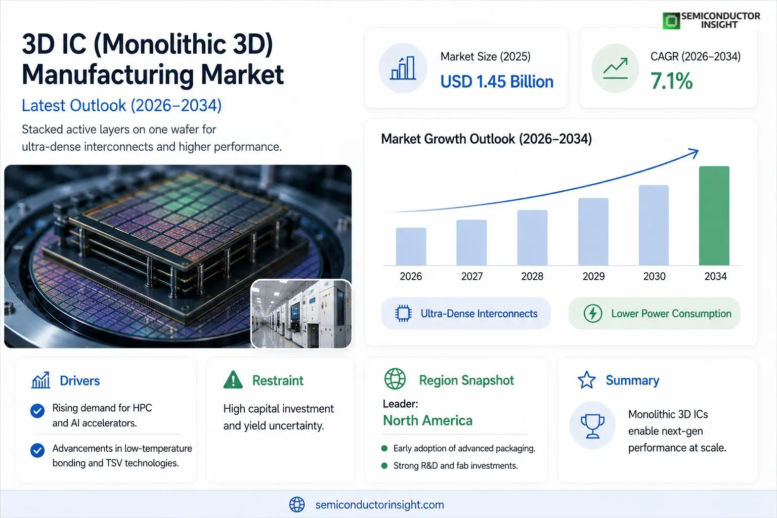
Global 3D IC (Monolithic 3D) Manufacturing Market size was valued at USD 1.45 billion in 2025. The market is projected to grow from USD 1.58 billion in 2026 to USD 2.73 billion by 2034, exhibiting a CAGR of 7.1% during the forecast period.
Monolithic 3D IC manufacturing involves stacking multiple active device layers on a single silicon wafer using sequential deposition and patterning processes, enabling ultra‑dense interconnects and a reduced form‑factor compared with traditional planar or heterogeneous integration approaches.The market is experiencing rapid expansion because semiconductor demand for high‑performance computing, AI accelerators, and mobile devices continues to rise. Furthermore, advancements in low‑temperature wafer bonding and through‑silicon‑via (TSV) technologies are lowering production costs. Key players such as Intel, TSMC, Samsung Electronics, and GlobalFoundries are accelerating development programs and forming strategic alliances to capture emerging opportunities.
MARKET DRIVERS
Technology Maturation
The rapid maturation of monolithic stacking techniques,such as via‑first transistor formation and wafer‑scale bonding,has lowered defect density, enabling higher yields for 3D IC (Monolithic 3D) Manufacturing Market. Industry pilots demonstrate that die‑to‑die interconnect pitch can now be reduced to sub‑20 nm, which directly drives adoption in high‑performance compute.
Demand from AI & Edge Computing
AI accelerators and edge devices require exceptionally dense interconnects and low‑latency memory access. Monolithic 3D offers a path to integrate logic and memory within a single substrate, meeting the power‑efficiency targets set by next‑generation applications. Consequently, OEMs are prioritizing this technology in their roadmaps.
➤ “By 2028, monolithic 3D is projected to capture over 15% of new AI‑focused chip designs, reshaping the manufacturing landscape.”
Regulatory incentives for energy‑efficient semiconductor production in major economies further reinforce investment, positioning 3D IC (Monolithic 3D) Manufacturing Market for sustained growth over the next decade.
MARKET CHALLENGES
Process Integration Complexity
Integrating multiple device layers without compromising thermal budgets remains a major engineering hurdle. Variations in material coefficients of thermal expansion can lead to wafer warpage, increasing cycle time and cost.
Other Challenges
Capital Intensity
Building dedicated monolithic 3D fabs requires multi‑billion‑dollar investments, limiting participation to well‑capitalized players and creating entry barriers for new entrants.
MARKET RESTRAINTS
Yield Uncertainty
Yield rates for monolithic stacks are still volatile compared with conventional planar processes. Limited historical data makes forecasting difficult, prompting cautious spend from risk‑averse manufacturers.
Supply Chain Constraints
The specialized consumables,such as high‑precision alignment tools and advanced dielectric materials,are sourced from a narrow supplier base, which can disrupt production if any single source faces shortages.
MARKET OPPORTUNITIES
Emerging Applications in 5G Infrastructure
5G base stations demand ultra‑compact RF front‑ends with integrated power management. Monolithic 3D provides a unique solution by stacking RF and digital blocks, opening new revenue streams for manufacturers willing to adapt their lines.
Strategic Partnerships
Collaborations between fabless designers and equipment vendors are accelerating the co‑development of process kits, reducing time‑to‑market and creating scalable business models for 3D IC (Monolithic 3D) Manufacturing Market.
3D IC (Monolithic 3D) Manufacturing Market Trends
Accelerating Adoption in High‑Performance Computing and AI
The shift toward monolithic 3D integration is being driven by the relentless demand for higher compute density in data‑center processors, artificial‑intelligence accelerators, and premium mobile silicon. By stacking multiple active device layers on a single silicon wafer, manufacturers achieve a three‑dimensional interconnect density that far exceeds planar alternatives, resulting in shorter signal paths, reduced latency, and lower power consumption per operation. This architectural advantage aligns closely with the performance‑per‑watt targets set by leading chipset designers, prompting early‑stage adoption in flagship products and stimulating a cascade of secondary investments across the ecosystem. As design teams incorporate 3D‑aware floor‑planning tools, the perceived risk of transitioning to vertical integration diminishes, reinforcing a virtuous cycle of design‑win and manufacturing‑scale that is reshaping the competitive landscape of advanced semiconductor manufacturing.
Other Trends
Cost‑Reduction Through Low‑Temperature Wafer Bonding and TSV Enhancements
Recent process innovations in low‑temperature wafer bonding have dramatically lowered the thermal budget required to join stacked layers, thereby reducing defectivity and enabling the reuse of existing equipment platforms. Coupled with advances in through‑silicon‑via (TSV) drilling precision and metallization reliability, these improvements translate into measurable cost savings per wafer and a higher overall yield profile. The net effect is a more attractive economics case for volume production, allowing manufacturers to extend monolithic 3D solutions beyond niche high‑end devices into broader product categories such as automotive electronics and edge‑computing modules. Moreover, the reduced thermal stress associated with low‑temperature bonding minimizes wafer warpage, which in turn improves lithographic alignment accuracy for subsequent patterning steps.
Strategic Alliances and Roadmap Consolidation Among Industry Leaders
Key players,including Intel, TSMC, Samsung Electronics, and GlobalFoundries,are actively forging strategic alliances, joint development agreements, and shared research initiatives to accelerate the maturation of monolithic 3D technology. These collaborations focus on standardizing interlayer interface specifications, scaling stack counts to four or more tiers, and integrating advanced materials that enhance electrical performance while maintaining mechanical stability. By aligning roadmaps and pooling R&D resources, the consortium of leaders is able to address common challenges such as thermal management, defect inspection, and process variation control more efficiently than isolated efforts. The resulting ecosystem of shared expertise and coordinated investment is expected to streamline time‑to‑market for next‑generation 3D IC products, reinforcing the market’s upward trajectory through the end of the decade.
COMPETITIVE LANDSCAPEKey Industry Players
Emerging Leaders in Monolithic 3D IC Manufacturing
Monolithic 3‑D IC market is currently dominated by a handful of integrated circuit powerhouses that have the scale to invest in low‑temperature wafer bonding, advanced patterning, and through‑silicon‑via (TSV) processes. Intel leverages its 3‑D silicon‑on‑insulator (SOI) roadmap to deliver high‑performance compute platforms, while TSMC’s 3‑D integration services support leading AI accelerator designers. Samsung Electronics accelerates volume production through its mature foundry lines, and GlobalFoundries provides a differentiated offering for automotive and edge applications. These four firms shape the overall market structure, dictate pricing benchmarks, and drive the majority of R&D spend, creating a tiered ecosystem where smaller players gravitate toward niche or collaborative roles.Beyond the tier‑one group, several specialized manufacturers and service providers enrich the competitive landscape. Amkor Technology and ASE Group offer advanced packaging and wafer‑level integration that complement monolithic stacking. STMicroelectronics and Infineon focus on power‑efficient 3‑D solutions for automotive and industrial IoT. IMEC and CEA‑Leti supply research‑scale process development, while TowerJazz (now part of GlobalFoundries) maintains legacy specialty nodes. Additional contributors include Renesas, NXP Semiconductors, Sony Semiconductor Solutions, Qualcomm, and Applied Materials (as a key equipment supplier). Their collective activities broaden the supply chain, encourage standards adoption, and enable customers to access monolithic 3‑D technologies without relying solely on the four dominant foundries.
List of Key 3D IC (Monolithic 3D) Manufacturing Market Companies Profiled
- Intel Corporation
- TSMC
- Samsung Electronics
- GlobalFoundries
- Amkor Technology
- ASE Group
- STMicroelectronics
- Infineon Technologies
- IMEC
- Renesas Electronics
- NXP Semiconductors
- Sony Semiconductor Solutions
- Qualcomm
- Applied Materials
Segment Analysis:
| Segment Category | Sub-Segments | Key Insights |
| By Type |
|
Wafer‑Level Monolithic Stacking
|
| By Application |
|
Artificial Intelligence Accelerators
|
| By End User |
|
Chip Designers
|
| By Process Technology |
|
Low‑Temperature Deposition
|
| By Market Driver |
|
Demand for Miniaturization
|
Regional Analysis: North America
United States
The adoption of chiplet designs is rapidly gaining traction in the US, enabling modularity and scalability in 3D IC manufacturing.
Significant government programs are supporting research and development in advanced packaging and 3D integration.
The demand for enhanced computing power in various sectors is driving investment in 3D IC for HPC applications.
The US is at the forefront of developing and implementing advanced packaging technologies for 3D IC.
Europe
Europe’s 3D IC (Monolithic 3D) Manufacturing Market is experiencing steady growth, driven by strong demand from automotive, industrial, and aerospace sectors. While not yet at the level of the US, Europe possesses a strong foundation in semiconductor design and manufacturing. Collaboration between European research institutions and industry players is crucial for advancing 3D integration capabilities. Business strategies in Europe often focus on developing niche applications and leveraging existing manufacturing infrastructure. The European Union’s initiatives to bolster domestic semiconductor production are expected to further stimulate growth in this area. The focus is on enhancing power efficiency and reliability in 3D IC for various applications.
Asia-Pacific
Asia-Pacific, particularly Taiwan and South Korea, represents a significant and rapidly expanding market for 3D IC (Monolithic 3D) Manufacturing. The region benefits from a mature semiconductor ecosystem, established manufacturing capabilities, and strong government support. The demand originates from key industries like smartphones, consumer electronics, and high-performance computing. Business strategies are centered on scaling up production capacity and developing advanced packaging technologies. The emphasis is on cost competitiveness and rapid innovation. Asia-Pacific is becoming a dominant player in the global 3D IC market, investing heavily in research and manufacturing infrastructure.
South America
3D IC (Monolithic 3D) Manufacturing Market in South America is nascent but holds potential for growth. The increasing adoption of IoT devices, telecommunications infrastructure upgrades, and the expansion of the automotive industry are creating demand for advanced semiconductor solutions. Business strategies are focused on partnerships and technology transfer to build local capabilities. The market is characterized by a relatively small number of players and a focus on specific applications like embedded systems and industrial control.
Middle East & Africa
The Middle East & Africa region presents a relatively smaller but growing market for 3D IC (Monolithic 3D) Manufacturing. Investments in infrastructure development, digital transformation initiatives, and the expansion of the technology sector are driving demand. Business strategies involve localized manufacturing and partnerships to address regional needs. The focus is on applications like smart cities, renewable energy, and industrial automation. The region is expected to witness increased adoption of 3D IC in the coming years.
Report Scope
This market research report provides a comprehensive analysis of the 3D IC (Monolithic 3D) Manufacturing Market , covering the forecast period 2026–2034. It offers detailed insights into market dynamics, technological advancements, competitive landscape, and key trends shaping the industry.
Key focus areas of the report include:
- Market Overview: The report begins with an overview outlining its current market scenario, key growth indicators, and industry transformation drivers. It discusses macroeconomic factors, demand–supply balance, regulatory landscape, and the strategic role of semiconductors in powering advancements across industries such as automotive, telecommunications, consumer electronics, and industrial automation.
- Market Size & Forecast: Historical data and future projections for revenue, unit shipments, and market value across major regions and segments.
- Segmentation Analysis: Detailed breakdown by product type, technology, application, and end-user industry to identify high-growth segments and investment opportunities.
- Regional Insights: Insights into market performance across North America, Europe, Asia-Pacific, Latin America, and the Middle East & Africa, including country-level analysis where relevant.
- Competitive Landscape: Profiles of leading market participants, including their product offerings, R&D focus, manufacturing capacity, pricing strategies, and recent developments such as mergers, acquisitions, and partnerships.
- Technology Trends & Innovation: Assessment of emerging technologies, integration of AI/IoT, semiconductor design trends, fabrication techniques, and evolving industry standards.
- Market Drivers & Restraints: Evaluation of factors driving market growth along with challenges, supply chain constraints, regulatory issues, and market-entry barriers.
- Stakeholder Insights: Insights for component suppliers, OEMs, system integrators, investors, and policymakers regarding the evolving ecosystem and strategic opportunities.
FREQUENTLY ASKED QUESTIONS:
What is the current market size of 3D IC (Monolithic 3D) Manufacturing Market?
-> 3D IC (Monolithic 3D) Manufacturing Market was valued at USD 1.45 billion in 2025 and is expected to reach USD 2.73 billion by 2034.
Which key companies operate in 3D IC (Monolithic 3D) Manufacturing Market?
-> Key players include Intel, TSMC, Samsung Electronics, and GlobalFoundries, among others.
What are the key growth drivers?
-> Key growth drivers include rising demand for high‑performance computing, AI accelerators, mobile devices, and cost reductions from low‑temperature wafer bonding and through‑silicon‑via (TSV) technologies.
Which region dominates the market?
-> The market sees strong activity across North America, Asia‑Pacific, and Europe, with North America often leading in early adoption of advanced packaging technologies.
What are the emerging trends?
-> Emerging trends include advancements in low‑temperature wafer bonding, TSV integration, and monolithic stacking techniques that enable ultra‑dense interconnects.

Get Sample Report PDF for Exclusive Insights
Report Sample Includes
- Table of Contents
- List of Tables & Figures
- Charts, Research Methodology, and more...
 Download Sample Report PDF


