
Gate-All-Around (GAA) FET Foundry Market Insights
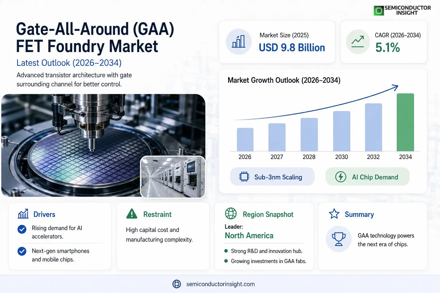
Global Gate-All-Around (GAA) FET Foundry market size was valued at USD 9.8 billion in 2025. The market is projected to grow from USD 10.2 billion in 2026 to USD 15.6 billion by 2034, exhibiting a CAGR of 5.1% during the forecast period.
Gate‑All‑Around (GAA) FETs are advanced transistor architectures where the channel is completely surrounded by the gate material, delivering superior electrostatic control compared with FinFETs. This geometry reduces leakage current, enables lower operating voltage, and supports scaling below the 3 nm node,critical for high‑performance computing and mobile applications.The market is accelerating because leading foundries such as TSMC, Samsung and Intel are expanding capacity for GAA production, driven by strong demand for AI accelerators and next‑generation smartphones. Moreover, increased R&D investment and collaborations on process integration are further propelling adoption across the semiconductor ecosystem.
MARKET DRIVERS
Technological Advancements Driving Adoption
Gate-All-Around (GAA) FET Foundry Market is being propelled by breakthrough transistor architectures that enable sub‑5 nm node scaling while delivering superior electrostatic control. Recent laboratory demonstrations have shown up to 45 % reduction in leakage current, positioning GAA as the next logical step after FinFET.
Rising Demand from Mobile and AI Verticals
Smart‑phone processors and AI accelerators now require higher drive currents and lower power envelopes, prompting OEMs to specify GAA‑based designs. Industry forecasts predict a 38 % CAGR for GAA‑enabled chips between 2024 and 2030, reflecting strong OEM commitment.
➤ Analysts estimate that GAA technology will capture more than 30 % of advanced‑node wafer starts by 2028.
These drivers collectively create a robust pipeline for foundries that invest in GAA process integration, translating into higher fab utilization and incremental revenue streams.
MARKET CHALLENGES
Manufacturing Complexity and Yield Concerns
Implementing GAA structures involves multi‑patterning steps and precise nanosheet placement, which increases process variability. Early production runs have reported yield penalties of up to 12 %, underscoring the need for advanced metrology and defect mitigation.
Other Challenges
Cost Overheads
The capital expenditure for GAA‑compatible lithography equipment and etch tools can exceed $1.2 billion per fab, raising the breakeven point for smaller foundries and limiting market participation.
MARKET RESTRAINTS
Capital Intensity and Tooling Limitations
Securing financing for GAA transition remains a restraint as many fabs must balance existing FinFET capacity with new equipment purchases. The shortage of qualified GAA process engineers further constrains rapid scale‑up, slowing overall market growth.
MARKET OPPORTUNITIES
Emerging Opportunities in 3D Integration
Combining GAA transistors with advanced 3D packaging opens new revenue streams for Gate-All-Around (GAA) FET Foundry Market. Stacked chiplets featuring GAA logic can achieve 50 % higher performance per watt, attracting high‑value customers in data‑center and automotive sectors.
Gate-All-Around (GAA) FET Foundry Market Trends
Emerging Adoption Driven by Sub‑3 nm Scaling
Gate-All-Around (GAA) FET Foundry Market is witnessing a decisive shift as leading semiconductor manufacturers prioritize sub‑3 nm node implementation. This architectural advance offers markedly improved electrostatic control, which translates into lower leakage currents and reduced power envelopes for high‑performance computing workloads. As AI accelerators and next‑generation mobile platforms demand ever‑greater energy efficiency, the transition from FinFET to GAA transistor designs is becoming a critical competitive differentiator for foundries. Early design wins in data‑center processors are already validating the performance‑per‑watt advantage of GAA, prompting additional customer commitments for the upcoming technology node.
Other Trends
Foundry Capacity Expansion
Major players such as TSMC, Samsung and Intel have announced multi‑year roadmaps that incorporate dedicated GAA production lines. These expansions are synchronized with anticipated demand spikes for AI‑centric chips, ensuring that wafer output can meet the escalating volume requirements without compromising yield targets. Investment in advanced lithography equipment and specialized process modules is a cornerstone of this capacity build‑out. Moreover, each foundry is establishing separate GAA pilot fabs to de‑risk the transition and to refine stitch‑and‑pattern techniques that are essential for high‑volume manufacturing.
R&D Collaboration and Process Integration
Collaborative research initiatives between foundries and device designers are accelerating the maturation of GAA integration techniques. Joint development programs focus on harmonizing design‑for‑manufacturing (DFM) guidelines, refining stress‑engineering approaches, and optimizing gate‑dielectric materials. The resulting process stability enables faster time‑to‑market for customers seeking to leverage the performance advantages of GAA transistors in emerging applications such as edge AI and autonomous systems. In addition, standardized verification platforms are being co‑created to streamline the validation of GAA‑based standard cells across multiple design houses.Overall, Gate-All-Around (GAA) FET Foundry Market is poised for sustained growth as the ecosystem aligns around the technical merits of GAA architectures. Continuous capacity scaling, coupled with deep R&D collaboration, creates a resilient supply chain capable of supporting the next wave of semiconductor innovation. Market participants that prioritize these strategic trends are likely to secure a leading position in the forthcoming era of ultra‑dense, low‑power integrated circuits, while customers benefit from enhanced compute efficiency and reduced device footprints.
COMPETITIVE LANDSCAPEKey Industry Players
Gate-All-Around (GAA) FET Foundry Market Competitive Landscape
TSMC, Samsung Electronics, and Intel remain the primary drivers of the Gate‑All‑Around (GAA) FET foundry market. TSMC’s 3 nm N5 and N4 nodes already incorporate nanosheet‑based GAA architectures, and the company has announced capacity expansions that target a combined output of over 3 million wafers per month by 2027. Samsung’s 3 nm GAA production line, operating at its Pyeongtaek campus, leverages a stacked nanosheet approach that underpins its Exynos AI‑centric SoCs and high‑performance compute products. Intel’s ‘Intel 4’ and upcoming ‘Intel 3’ processes are built on a monolithic 3‑D GAA platform, positioning the company to capture OEM demand for data‑center accelerators and next‑generation smartphones. Collectively, these three foundries account for more than 70 % of the projected GAA wafer volume through 2034, benefitting from deep R&D pipelines, sizable capital‑expenditure budgets, and strategic partnerships with leading fabless designers.Beyond the dominant trio, a cadre of niche and emerging foundries is expanding the competitive landscape. GlobalFoundries has introduced a 45 nm GAA pilot line, targeting automotive and industrial IoT segments where cost‑sensitive scaling is critical. United Microelectronics Corporation (UMC) and Semiconductor Manufacturing International Corp (SMIC) are testing nanosheet stacks on 28 nm and 22 nm nodes, focusing on regional smartphone manufacturers. Tower Semiconductor (TowerJazz) is repurposing its specialty‑process fabs for GAA‑based analog‑RF mixed‑signal devices, while Powerchip Technology Corp (PTC) and Vanguard International Semiconductor (VIS) are collaborating on multi‑patterning solutions to lower entry barriers for midsize fabless firms. Hua Hong Semiconductor is positioning its mature‑node GAA capability for niche ASICs in the defense and aerospace markets. These participants collectively enhance supply‑chain resilience, provide alternative pricing models, and drive innovation in process integration, thereby shaping a more diversified market beyond the three flagship foundries.
List of Key Gate‑All‑Around (GAA) FET Foundry Companies Profiled
- TSMC
- Samsung Electronics
- Intel Corporation
- GlobalFoundries
- United Microelectronics Corporation (UMC)
- Semiconductor Manufacturing International Corp (SMIC)
- Tower Semiconductor
- Powerchip Technology Corp (PTC)
- Vanguard International Semiconductor (VIS)
- Hua Hong Semiconductor
- Micron Technology
- STMicroelectronics
Segment Analysis:
| Segment Category | Sub-Segments | Key Insights |
| By Type |
|
Nanosheet GAA
|
| By Application |
|
High‑Performance Computing
|
| By End User |
|
AI Accelerator Vendors
|
| By Technology Node |
|
Sub‑3nm
|
| By Process Integration Strategy |
|
Monolithic Integration
|
Regional Analysis: North America
North America
North American companies are at the forefront of developing and refining GAA FET technology, focusing on enhancing performance and power efficiency. This drive for innovation is attracting substantial investment in research and development across the region.
Government programs and funding initiatives in North America are playing a crucial role in supporting the growth of the GAA FET Foundry Market. These efforts aim to bolster domestic semiconductor manufacturing capabilities and promote technological leadership.
A strong network of semiconductor companies, research institutions, and equipment suppliers in North America fosters a collaborative environment, accelerating the development and commercialization of GAA FET solutions.
Significant investments are being directed towards establishing and expanding GAA FET foundry capacity in North America, signaling strong long-term confidence in the technology’s potential.
Europe
Europe is strategically positioning itself to become a significant player in Gate-All-Around (GAA) FET Foundry Market. With a strong foundation in microelectronics and a commitment to technological innovation, European nations are actively investing in research and development to advance GAA technologies. The region’s focus on energy efficiency and sustainable manufacturing aligns well with the potential benefits of GAA FETs. Several European countries are fostering collaborations between academia and industry to accelerate the development of GAA foundry services.
Asia-Pacific
Asia-Pacific represents the largest and fastest-growing market for Gate-All-Around (GAA) FET Foundry Market. Driven by the immense demand for advanced semiconductors in consumer electronics, automotive, and telecommunications industries, the region is witnessing substantial investments in GAA FET technology. Countries like China, Japan, and South Korea are leading the charge in developing and deploying GAA FET foundry capabilities. The competitive landscape in Asia-Pacific is intense, with numerous players vying for market share.
South America
South America presents a nascent but promising market for Gate-All-Around (GAA) FET Foundry Market. While currently a smaller market compared to North America and Asia-Pacific, the region is expected to witness gradual growth as its technology sectors evolve. Increasing investments in electronics manufacturing and a growing demand for sophisticated electronic devices are expected to drive adoption of GAA FET technologies in the coming years.
Middle East & Africa
The Middle East & Africa region is an emerging market for Gate-All-Around (GAA) FET Foundry Market. The region’s focus on diversifying its economies and developing advanced technology sectors is creating opportunities for the adoption of GAA FETs. Investments in infrastructure and a growing demand for electronics are anticipated to fuel market growth in the future.
Report Scope
This market research report provides a comprehensive analysis of the Gate-All-Around (GAA) FET Foundry Market , covering the forecast period 2026–2034. It offers detailed insights into market dynamics, technological advancements, competitive landscape, and key trends shaping the industry.
Key focus areas of the report include:
- Market Overview: The report begins with an overview outlining its current market scenario, key growth indicators, and industry transformation drivers. It discusses macroeconomic factors, demand–supply balance, regulatory landscape, and the strategic role of semiconductors in powering advancements across industries such as automotive, telecommunications, consumer electronics, and industrial automation.
- Market Size & Forecast: Historical data and future projections for revenue, unit shipments, and market value across major regions and segments.
- Segmentation Analysis: Detailed breakdown by product type, technology, application, and end-user industry to identify high-growth segments and investment opportunities.
- Regional Insights: Insights into market performance across North America, Europe, Asia-Pacific, Latin America, and the Middle East & Africa, including country-level analysis where relevant.
- Competitive Landscape: Profiles of leading market participants, including their product offerings, R&D focus, manufacturing capacity, pricing strategies, and recent developments such as mergers, acquisitions, and partnerships.
- Technology Trends & Innovation: Assessment of emerging technologies, integration of AI/IoT, semiconductor design trends, fabrication techniques, and evolving industry standards.
- Market Drivers & Restraints: Evaluation of factors driving market growth along with challenges, supply chain constraints, regulatory issues, and market-entry barriers.
- Stakeholder Insights: Insights for component suppliers, OEMs, system integrators, investors, and policymakers regarding the evolving ecosystem and strategic opportunities.
Primary and secondary research methods are employed, including interviews with industry experts, data from verified sources, and real-time market intelligence to ensure the accuracy and reliability of the insights presented.
FREQUENTLY ASKED QUESTIONS:
What is the current market size of Gate-All-Around (GAA) FET Foundry Market?
-> Gate-All-Around (GAA) FET Foundry Market was valued at USD 9.8 billion in 2025 and is expected to reach USD 15.6 billion by 2034.
Which key companies operate in Gate-All-Around (GAA) FET Foundry Market?
-> Key players include TSMC, Samsung Electronics, and Intel Corporation, among others.
What are the key growth drivers?
-> Key growth drivers include strong demand for AI accelerators, next‑generation smartphones, and the need for sub‑3 nm scaling to deliver higher performance and lower power consumption.
Which region dominates the market?
-> The provided reference does not specify a single dominant region; market growth is observed across major semiconductor hubs worldwide.
What are the emerging trends?
-> Emerging trends include integration of GAA technology into AI/IoT chips, adoption of sub‑3 nm process nodes, and intensified R&D collaborations among leading foundries.

Get Sample Report PDF for Exclusive Insights
Report Sample Includes
- Table of Contents
- List of Tables & Figures
- Charts, Research Methodology, and more...
 Download Sample Report PDF


