GaN-On-SiC Epiwafer Market Insights
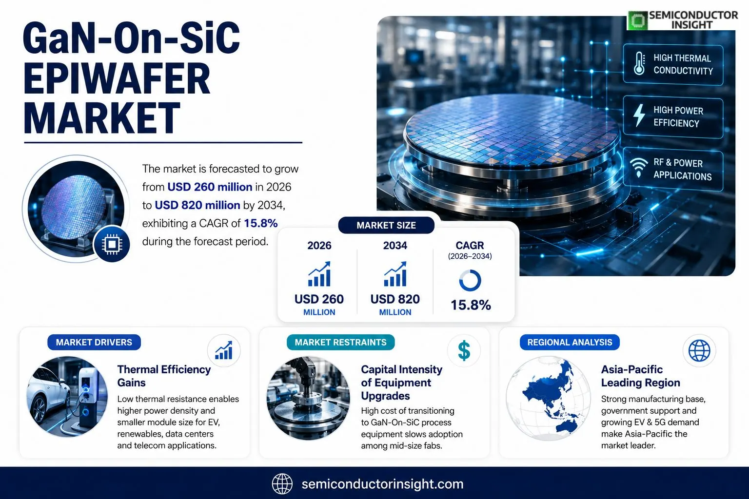
GaN-On-SiC Epiwafer market size was valued at USD 250 million in 2025. The market is forecasted to grow from USD 260 million in 2026 to USD 820 million by 2034, exhibiting a CAGR of 15.8% during the forecast period.
GaN‑On‑SiC epiwafers consist of gallium nitride layers epitaxially grown on silicon carbide substrates, offering high thermal conductivity and exceptional electron mobility that support both power conversion and radio‑frequency functions.The expansion reflects rising automotive electrification that requires more efficient power converters, alongside telecom upgrades that call for resilient RF front‑ends for emerging network standards. Recent collaborations underscore this momentum; in March 2024 Wolfspeed entered a joint development agreement with a major EV‑charging OEM to qualify eight‑inch SiC substrates for GaN growth. Companies such as NTT AT, IQE and Suzhou Nanowin are also extending their offerings, strengthening overall supply chain robustness.
MARKET DRIVERS
Thermal Efficiency Gains
The intrinsic low thermal resistance of gallium‑nitride on silicon‑carbide structures enables power converters to operate at higher current densities while maintaining safe junction temperatures. Manufacturers can therefore shrink module footprints and cut cooling‑system costs, a benefit that resonates across data‑center, renewable‑energy and electric‑vehicle applications. This technical advantage directly fuels demand for the GaN‑On‑SiC Epiwafer Market.
Supply‑Chain Maturation
Recent investments in 150‑mm wafer fabs have lifted annual capacity to well over 1 million wafers, while process‑optimization programs have lifted average yields from the mid‑60 % range to above 80 %. Higher yields translate into predictable pricing and shorter lead times, encouraging OEMs to replace legacy silicon devices with GaN‑On‑SiC solutions.
➤ “The convergence of thermal performance and scalable manufacturing is reshaping the power‑electronics value chain.”
Collectively, these forces create a virtuous cycle: as more system integrators certify GaN‑On‑SiC designs, downstream volume ramps, spurring further process refinements and cost reductions across the GaN‑On‑SiC Epiwafer Market.
MARKET CHALLENGES
Manufacturing Yield Variability
Despite progress in epitaxial growth, achieving uniform defect densities across 150‑mm substrates remains a technical hurdle. Yield fluctuations can erode margins for wafer suppliers, especially when early‑stage customers demand large‑volume runs. The uncertainty forces some manufacturers to retain safety stocks, inflating inventory costs.
Other Challenges
Cost Sensitivity
The premium price of GaN‑On‑SiC wafersoften 30‑40 % higher than comparable silicon carbide alternativeslimits adoption in price‑conscious segments such as consumer‑grade power adapters. Companies must therefore demonstrate clear total‑cost‑of‑ownership benefits to justify the upfront expense.
MARKET RESTRAINTS
Capital Intensity of Equipment Upgrades
Transitioning from silicon‑based lines to GaN‑On‑SiC process equipment requires multi‑million‑dollar capital outlays. Mid‑size fabs often lack the financial flexibility to absorb these expenditures, resulting in slower adoption curves and constraining the overall market expansion.
MARKET OPPORTUNITIES
Automotive Power‑Module Expansion
Electric‑vehicle powertrains demand converters that can handle >500 V while delivering >200 kW in compact packages. GaN‑On‑SiC epiwafers meet these specifications, opening a multi‑billion‑dollar revenue channel for suppliers that can certify automotive‑grade reliability. Early collaborations between wafer manufacturers and Tier‑1 automotive firms hint at a rapidly emerging niche within the GaN‑On‑SiC Epiwafer Market.
GaN-On-SiC Epiwafer Market Trends
Shift Toward Larger‑Diameter Epiwafers
The industry is migrating from the legacy 4‑inch and 6‑inch platforms toward 8‑inch SiC substrates, a move that reshapes supply‑chain economics and device performance limits. Larger diameters cut per‑unit material waste, allowing manufacturers to lower the cost per watt for high‑power devices while delivering tighter defect control. This transition is also unlocking new design geometries for RF amplifiers, where higher breakdown voltage translates directly into higher linearity. Companies that have already re‑tooled their epitaxial reactors report faster cycle times and a measurable improvement in yield, creating a competitive edge for early adopters of the 8‑inch format within the GaN‑On‑SiC Epiwafer Market.
Other Trends
Expansion of Chinese SiC Supply Chains
China’s semiconductor ecosystem is rapidly broadening its footprint in SiC wafer production, and that expansion reverberates through the GaN‑On‑SiC value chain. Domestic manufacturers are scaling capacity at multiple sites, benefitting from coordinated government incentives and a growing talent pool focused on wide‑bandgap materials. The result is a more diversified supplier base, which reduces reliance on traditional hubs in the United States, Europe, and Japan. For system integrators, the emergence of Chinese players introduces alternative pricing structures and accelerates time‑to‑market for next‑generation power converters, especially in electric‑vehicle platforms where cost sensitivity is paramount.
Application Diversification into RF and Power Electronics
Beyond conventional power‑conversion modules, designers are increasingly embedding GaN‑On‑SiC epiwafers into high‑frequency RF front‑ends for 5G and satellite communications. The hybrid material stack offers a rare combination of high electron mobility and superior thermal conductivity, enabling amplifiers that operate at higher frequencies without compromising reliability. Simultaneously, data‑center power supplies are adopting the same technology to push efficiency thresholds above 98 % while managing dense thermal loads. This dual‑application trajectory creates a feedback loop: improvements in one segment spill over into the other, prompting equipment makers to align R&D roadmaps and investors to allocate resources across both power and RF domains.
COMPETITIVE LANDSCAPEKey Industry Players
Competitive Dynamics of the GaN‑On‑SiC Epiwafer Segment
Wolfspeed commands a decisive share of the GaN‑On‑SiC epiwafer market, leveraging its vertically integrated production line that spans from 6‑inch SiC substrate growth to device‑ready GaN layers. This end‑to‑end capability grants Wolfspeed pricing leverage and short lead‑times, letting it dominate high‑volume power‑electronics contracts for automotive inverter modules. NTT AT follows closely, differentiating through advanced epitaxial engineering that improves thermal conductivity and breakdown voltage, making its wafers attractive for RF power amplifiers in 5G infrastructure. Both firms anchor the market structure, forcing newer entrants to pursue niche alloy compositions or specialized wafer diametersparticularly the emerging 8‑inch segment that promises higher throughput for EV‑centric power stages. The competition pivots on yield optimization, substrate cost management, and the ability to scale from pilot to full‑scale manufacturing without sacrificing crystalline quality.Beyond the front‑runners, a coalition of Asian and European players adds depth to the competitive set. Sumitomo’s SCIOCS unit supplies premium 4‑inch wafers prized for research labs, while Soitec’s EpiGaN line focuses on mixed‑mode devices that blend power and RF performance. IQE offers a diversified portfolio that includes custom epitaxy services for niche applications such as satellite communications. Chinese firmsSuzhou Nanowin, Shanxi Yuteng, and GLChave accelerated capacity expansion, targeting domestic EV manufacturers and benefitting from state‑backed subsidies. Enkris Semiconductor and CorEnergy round out the field with boutique solutions for high‑frequency radar and defense markets, where performance margins outweigh cost considerations.
List of Key GaN‑On‑SiC Epiwafer Companies Profiled
- Wolfspeed
- NTT AT
- Sumitomo (SCIOCS)
- Soitec (EpiGaN)
- IQE
- Enkris Semiconductor Inc
- CorEnergy
- GLC
- Suzhou Nanowin
- Shanxi Yuteng
- Advanced Semiconductor Materials Ltd
- Tokyo Electronics
- EuroGaN Technologies
Segment Analysis:
| Segment Category | Sub-Segments | Key Insights |
| By Type |
|
Leading Segment – 6‑inch
|
| By Application |
|
Leading Segment – Electronic Power
|
| By End User |
|
Leading Segment – Power‑electronics OEMs
|
| By Technology Maturity |
|
Leading Segment – Established Products
|
| By Market Drivers |
|
Leading Driver – Energy‑efficiency mandates
|
Regional Analysis: GaN-On-SiC Epiwafer Market
Asia-Pacific
A tight cluster of wafer growers, metallization specialists, and testing labs in Taiwan and Singapore creates a low‑latency pipeline that trims lead times. This concentration not only reduces logistics costs but also enables rapid feedback loops for process tweaks, giving the region a decisive edge in time‑to‑market.
National semiconductor roadmaps in China and Japan earmark multi‑billion‑dollar funds for GaN‑On‑SiC R&D, while tax breaks accelerate capital investment in epitaxial tooling. Such policy scaffolding translates into a predictable environment for long‑range project financing.
Collaborative university‑industry consortia are publishing breakthrough papers on defect mitigation and substrate thinning. These initiatives pull knowledge from academia into production lines, shortening the gap between prototype and volume.
The region’s aggressive roll‑out of 5G and electric‑vehicle platforms creates immediate pull for high‑power GaN‑On‑SiC modules, prompting OEMs to lock in supply agreements well ahead of full market saturation.
North America
The United States and Canada are leveraging deep pockets of venture capital to nurture niche players focused on high‑frequency communication chips. While the domestic supply chain is less consolidated than in Asia‑Pacific, strong intellectual‑property protections encourage proprietary process development. Federal initiatives targeting clean‑energy transition are channeling funds toward GaN‑On‑SiC for grid‑level inverters, yet the relative scarcity of large‑scale epitaxy facilities forces many firms to outsource wafer production abroad, introducing a dependency that shapes sourcing strategies.
Europe
European stakeholders are emphasizing sustainability and regulatory compliance, positioning GaN‑On‑SiC as a key enabler for low‑emission transport and industrial automation. Germany’s “Industrial 4.0” framework incentivizes pilot lines that integrate GaN devices into power‑train prototypes, while the Nordic region invests in research clusters that explore thermally robust packaging. However, the fragmented manufacturing base across borders mandates cross‑border collaborations, which can lengthen decision cycles but also stimulate standard‑setting efforts.
South America
Growth in Brazil’s renewable‑energy sector is creating a modest appetite for efficient power converters, prompting local distributors to seek GaN‑On‑SiC solutions. Limited in‑region fabrication capability means the market relies heavily on imports, a factor that keeps price sensitivity high. Companies are therefore concentrating on value‑added services such as design‑for‑manufacturability consulting to differentiate themselves in a price‑driven environment.
Middle East & Africa
The Gulf Cooperation Council nations view GaN‑On‑SiC as a strategic technology for data‑center expansion and oil‑field electrification, where reliability under extreme temperatures is paramount. Investment funds are earmarking capital for pilot production cells, yet the absence of a mature supply ecosystem forces reliance on partnerships with Asian manufacturers. In Africa, nascent telecom roll‑outs are sparking interest in compact, high‑efficiency amplifiers, laying the groundwork for future demand as connectivity projects scale.
Report Scope
This market research report provides a comprehensive analysis of the GaN-On-SiC Epiwafer Market , covering the forecast period 2026–2034. It offers detailed insights into market dynamics, technological advancements, competitive landscape, and key trends shaping the industry.
Key focus areas of the report include:
- Market Overview: The report begins with an overview outlining its current market scenario, key growth indicators, and industry transformation drivers. It discusses macroeconomic factors, demand–supply balance, regulatory landscape, and the strategic role of semiconductors in powering advancements across industries such as automotive, telecommunications, consumer electronics, and industrial automation.
- Market Size & Forecast: Historical data and future projections for revenue, unit shipments, and market value across major regions and segments.
- Segmentation Analysis: Detailed breakdown by product type, technology, application, and end-user industry to identify high-growth segments and investment opportunities.
- Regional Insights: Insights into market performance across North America, Europe, Asia-Pacific, Latin America, and the Middle East & Africa, including country-level analysis where relevant.
- Competitive Landscape: Profiles of leading market participants, including their product offerings, R&D focus, manufacturing capacity, pricing strategies, and recent developments such as mergers, acquisitions, and partnerships.
- Technology Trends & Innovation: Assessment of emerging technologies, integration of AI/IoT, semiconductor design trends, fabrication techniques, and evolving industry standards.
- Market Drivers & Restraints: Evaluation of factors driving market growth along with challenges, supply chain constraints, regulatory issues, and market-entry barriers.
- Stakeholder Insights: Insights for component suppliers, OEMs, system integrators, investors, and policymakers regarding the evolving ecosystem and strategic opportunities.
Primary and secondary research methods are employed, including interviews with industry experts, data from verified sources, and real-time market intelligence to ensure the accuracy and reliability of the insights presented.
FREQUENTLY ASKED QUESTIONS:
What is the current market size of GaN-On-SiC Epiwafer Market?
-> GaN-On-SiC Epiwafer Market was valued at USD 226 million in 2024 and is expected to reach USD 897 million by 2031, at a CAGR of 22.3% during the forecast period.
Which key companies operate in GaN-On-SiC Epiwafer Market?
-> Key players include NTT AT, Wolfspeed, SCIOCS (Sumitomo), EpiGaN (Soitec), IQE, Enkris Semiconductor Inc, CorEnergy, GLC, Suzhou Nanowin, Shanxi Yuteng.
What are the key growth drivers?
-> Key growth drivers include strong demand from electric vehicles (EV), rapid adoption of 6‑inch SiC substrates, upcoming transition to 8‑inch SiC wafers, and increased investments in power electronics and RF applications.
Which region dominates the market?
-> Asia is expected to dominate, driven by extensive SiC wafer production in China, Japan, and South Korea, with Chinese companies projected to play a pivotal role over the next ten years.
What are the emerging trends?
-> Emerging trends include scaling to 8‑inch SiC epitaxy, integration of GaN-on-SiC in high‑efficiency power converters, and expanding applications in RF and wireless communication systems.
Get Sample Report PDF for Exclusive Insights
Report Sample Includes
- Table of Contents
- List of Tables & Figures
- Charts, Research Methodology, and more...
 Download Sample Report PDF