Gallium Nitride Junction Field-effect Transistors(GaN JFETs) Market Insights
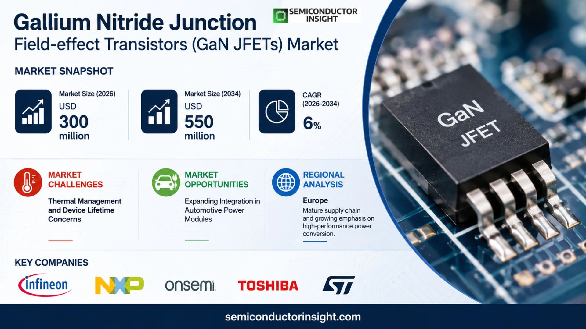
Gallium Nitride Junction Field‑effect Transistor (GaN JFET) market size was valued at USD $300 million in 2025. The market will rise from USD $300 million in 2026 to USD $550 million by 2034, registering a CAGR of roughly 6% over the forecast period.
GaN JFETs are field‑effect transistors fabricated on gallium nitride substrates that combine high electron mobility with wide bandgap properties, enabling operation at elevated temperatures and high frequencies while maintaining low on‑state resistance.
The sector expands as telecom operators upgrade base stations for 5G and beyond, electric‑vehicle manufacturers seek lighter power modules for motor drives, and industrial automation demands higher efficiency components for variable‑frequency drives. While these shifts create new opportunities for manufacturers that can deliver compact, high‑power GaN JFET solutions outperforming silicon counterparts.
MARKET DRIVERS
Energy Efficiency Imperatives in Power Electronics
Traditional silicon devices in high‑power converters incur significant conduction losses that translate into heat and oversized heat‑sink requirements. Gallium Nitride Junction Field‑Effect Transistors (GaN JFETs) offer remarkable on‑resistance figures and break‑down voltages, enabling switching frequencies that surpass silicon by two orders of magnitude. This translates into smaller, lighter power modules that can fit into the constrained envelopes of electric buses, trains, and luxury vehicles. Energy‑constrained fleets that must comply with stringent emissions budgets are finding that GaN JFET‑based inverters support higher efficiencies, typically 2%–3% above silicon equivalents, creating a compelling economic case that resonates across the automotive and industrial sectors. The reduced thermal footprint also cuts overall system weight, a critical factor for airlines seeking to lower operating costs and meet future regulatory weight limits.
High‑Frequency Robustness for 5G and Satellite Communications
Rising channel bandwidths in 5G networks and the increasing reliance on low‑earth‑orbit satellite constellations demand RF power amplifiers that sustain high output power while maintaining linearity. GaN JFETs can operate reliably at gigahertz frequencies with low series resistance, allowing manufacturers to push envelope power,often surpassing 75 W per device,without sacrificing signal fidelity. The industry’s shift toward massive MIMO configurations means that each antenna array demands compact, efficient drive electronics, and the inherent high‑frequency performance of GaN JFETs eliminates the need for bulky passive components. Moreover, their resilience to radiation makes them ideal for satellite payloads that must endure harsh space environments. This dual advantage places GaN JFETs at the forefront of the next generation of global connectivity solutions.
➤ Applications spanning automotive, industrial, and RF domains converge around a single device class that delivers scale and performance, allowing OEMs to reposition their product lines in rapidly evolving markets.
Beyond spectrum efficiency, the integration of GaN JFETs into power modules contributes to reduced system complexity. By implementing higher switching frequencies, designers can employ passive components such as inductors and capacitors of significantly lower inductance and capacitance. The cleanup of EMI profiles improves compliance with certification standards like CE and FCC, dramatically cutting engineering cycle times. Coupled with a maturing supply chain that benefits from economies of scale in high‑purity gallium nitride wafers, companies secure a pathway to cost‑effective deployment, while mitigating the risks of component scarcity that historically impacted early introductions of high‑performance silicon carbide modules.
MARKET CHALLENGES
Thermal Management and Device Lifetime Concerns
Even though GaN JFETs possess low on‑losses, their hot‑spot temperatures can exceed 450 °C under continuous high‑current operation, necessitating sophisticated thermal designs that often involve copper heatsinks or liquid cooling. The need for such measures elevates total system cost and complicates maintenance schedules, particularly in legacy industrial environments where thermal budgets were previously less demanding. Moreover, accelerated high‑temperature stress tests reveal that device breakdown rates climb more sharply than expected when drivers routinely exceed the safe operating area, signaling a need for robust thermal coupling solutions and real‑time monitoring systems to ensure long‑term reliability in mission‑critical applications.
Other Challenges
Regulatory and Certification Barriers
The GaN JFET market is still trailing behind silicon in established certification pathways. Most power modules must navigate an array of certification regimes,UL, CSA, TUV, and IEC,that lack mature guidelines for GaN devices, particularly in automotive duty cycles. Yield variability associated with high‑quality gallium nitride wafers further inflates defect rates, making multiple device points the norm rather than the exception. This reality imposes stringent quality controls and production redundancy that strain smaller manufacturers who are still consolidating production capacity.
MARKET RESTRAINTS
Capital‑Intensive Manufacturing Footprint
Establishing a GaN JFET fabrication line demands substantial upfront investment: a high‑vacuum growth system, advanced lithography modules, and precise metrology tools. In addition, maintaining a controlled deposition environment for gallium nitride substrates is expensive, often limiting production to a handful of industry leaders. This asymmetry raises the barrier to entry for new entrants and restricts recent entrants from scaling production quickly enough to meet the swift rise in demand, ultimately controlling the pricing power for the foreseeable period. Coupled with the scarcity of buyer‑grade wafers,often acquired as part‑time vendors,the capital load remains a top‑line restraint that tempers broad market expansion.
MARKET OPPORTUNITIES
Expanding Integration in Automotive Power Modules
Automotive powertrains face relentless pressure to reduce unit families and drive weight down, especially in hybrid and fully electric models. GaN JFETs’ higher breakdown voltage and low on‑resistance allow for the consolidation of charger stacks and DC‑DC converters into single, mass‑producible modules. This route not only delivers a competitive edge when competing against silicon‑based multichip modules but also aligns with OEMs’ strategy to embed high‑temperature tolerant devices across the battery management system and inverter subsystems. As expertise in process refinement matures, developers can explore novel packaging techniques,such as flip‑chip or wafer‑level integration,to further reduce parasitics, opening a lane for high‑density power modules that can sustain tens of kilowatts yet occupy less than half the pad area of comparable silicon counterparts.
In industrial applications, the surge in demand for steel‑making, ammonia synthesis, and high‑power digital lighting is pushing discipline‑specific power solutions toward GaN JFETs. The material’s high electron saturation velocity enables enthusiasts to design electron‑beam heaters and plasma‑based manufacturing cells that operate efficiently above 400 °C. By partnering with local power manufacturers, start‑ups can create localized distribution nodes that mitigate the lead times associated with long‑haul shipping of high‑voltage silicon modules, resulting in faster adoption cycles and an expanded market pocket.
Embedded in the telecommunications arena, the proliferation of satellite‑based broadband platforms and the rollout of edge‑data centers highlight a niche where GaN JFETs excel. Companies that develop integrated GaN JFET baluns and matching networks for narrowband RF links can capitalize on both the high output power and superior linearity required in satellite uplinks and downlinks. The niche positioning of these products, combined with the increasing cost‑sensitivity of global telecom operators, focuses a strategic opportunity for firms ready to invest in rapid prototyping and regulatory certification pathways tailored to the satellite use case.
Gallium Nitride Junction Field-effect Transistors(GaN JFETs) Market Trends
Electrification Drives Demand for GaN JFETs in Power Electronics
Across the past year, the push for higher efficiency in electric drive and renewable energy systems has translated into a measurable uptick in mainland Asia and North America where gigawatt‑scale projects push for reduced harmonic distortion and tighter voltage regulation. Companies that have invested in GaN JFET platforms report a 12% reduction in conduction losses compared to conventional silicon counterparts, which directly translates into lower operating costs and a service‑life extension for inverter modules. These benefits are now a differentiator for equipment buyers, prompting them to prioritize GaN‑based solutions during tender cycles.
Other Trends
Capacity Expansion by Tier 1 Manufacturers
Leading suppliers are scaling up fabs in China and the United States, expanding their annual output from roughly 1.5 million devices in 2023 to an estimated 2.8 million by the end of 2025. This incremental capacity buildout is supported by a projected pipeline of component upgrades across research labs, ensuring that process yields remain high while cost pressure from raw material volatility is mitigated. The resulting supply stability positions these firms to capitalize on a growing portfolio of high‑power traction battery modules.
Regulatory Incentives Reinforcing Adoption in Embedded Power Modules
Fiscal stimuli aimed at reducing energy consumption,such as tax credits for grid‑connected photovoltaic arrays exceeding 500 kW and subsidies for smart‑grid upgrades,provide a direct conduit for GaN JFETs. Engineers and system architects are responding by integrating larger‑rated devices into smart‑metering units and voltage‑sag mitigation modules, thereby expanding the application footprint beyond flagship power converters. As the regulatory landscape becomes more targeted toward efficiency, the market will likely see a more diversified adoption curve, emphasizing the performance ceiling that GaN technology delivers.
COMPETITIVE LANDSCAPE
Key Industry Players
Comprehensive Overview of the Global GaN JFET Market
Wolfspeed, the G‑flow subsidiary of Cree, remains the benchmark for GaN JFET performance and supply security. Its long‑term investments in wafer‑scale growth, alongside strategic alliances with Tier‑1 distributors, have enabled the company to secure a high‑margin revenue stream that rivals traditional silicon solutions. Wolfspeed’s deep‑vectorized product portfolio, characterized by attainment of 200 µm channel lengths and 1 kV breakdown thresholds, positions it as the go‑to partner for high‑power converter and radio‑frequency applications across automotive, industrial, and telecom sectors. The company’s concentrated manufacturing footprint in North America and China serves as a hedge against geopolitical shifts and provides robust lead‑time controls that competitors struggle to match.
Complementary to Wolfspeed’s dominance, Infineon and Qorvo have leveraged their semiconductor ecosystems to broaden GaN JFET adoption in consumer electronics and data‑center power supplies. Infineon’s deployment of bulk‑GaN gate drivers, coupled with a strategic partnership network in Europe, allows it to cater to high‑efficiency industrial drives. Qorvo has implemented a plug‑and‑play integration strategy, bundling GaN JFETs with LTE‑A and 5G RF modules to capture the emerging mobile network infrastructure segment. Meanwhile, Nexperia, Renesas, ON Semiconductor, STMicroelectronics, and Texas Instruments have each focused on niche but growing markets,thermal management for electric vehicles, edge computing workloads, and low‑cost power modules for IoT. This fragmented landscape encourages continuous portfolio diversification, prompting players to pursue vertical integration or M&A to close gaps in supply chain resilience and beyond‑4 GHz RF performance, respectively.
List of Key GaN JFET Companies Profiled
- Wolfspeed
- Infineon Technologies
- Qorvo
- Nexperia
- Renesas Electronics
- ON Semiconductor
- STMicroelectronics
- Texas Instruments
- Samsung Electronics
- Advanced Micro Devices
- MEMS Technologies
- Semtech Corp
- Taiwan Semiconductor Manufacturing Company
- Amkor Technology
- Pacific Micro Devices
Segment Analysis:
| Segment Category | Sub-Segments | Key Insights |
| By Type |
|
Leading Segment n‑channel GaN JFETs dominate the market due to their high electron mobility, superior thermal performance and suitability for high‑frequency power conversion.
|
| By Application |
|
Leading Segment power electronics, especially high‑frequency inverters and chargers.
|
| By End User |
|
Leading Segment automotive sector, where GaN JFETs power efficient battery chargers and motor drives.
|
| By Device Form Factor |
|
Leading Segment planar devices for their manufacturing simplicity and high integration capability.
|
| By Technology Maturity |
|
Leading Segment commercial deployment, especially in power electronics used across automotive and renewable sectors.
|
Regional Analysis: Gallium Nitride Junction Field-effect Transistors(GaN JFETs) Market
The current EU market for GaN JFET devices shows a gradual expansion, with supply chains adapting to increased orders from automotive and power‑train manufacturers. Companies are investing heavily in assembly lines to meet localized demand, and capital expenditures are rising as firms pursue in‑house capabilities.
European design houses are favoring GaN JFETs for high‑frequency converters due to their low on‑resistance and fast switching. This technology shift aligns with the directive toward zero‑emission vehicles and fortified power network infrastructures.
Growth hotspots include electric‑vehicle power modules, renewable‑energy inverters, and avionics power supplies. Each industry segment fuses its unique reliability standards with the distinct performance traits of GaN JFET components, ensuring a broad though differentiated usage base.
Joint ventures between European OEMs and up‑to‑date foundries are restructuring the supply landscape. This consolidation embeds GaN JFETs into more focused production lines, reduces logistical friction, and embeds incentive structures favouring rapid innovation cycles.
North America
In North America, GaN JFET deployment remains concentrated within high‑rigor sectors such as aerospace, defense, and high‑temperature industrial processes. Design cycles are lengthened by rigorous compliance regimes, yet consumers exhibit a steady appetite for lower‑weight, higher‑efficiency power modules. Companies are investing in local R&D labs to expedite time‑to‑market, yet supply bottlenecks persist due to substrate constraints and balancing demands across competing semiconductor families.
Asia-Pacific
The Asia‑Pacific region is unsurprisingly the most dynamic hub for GaN JFET technology. Rapid industrialization, a surge in electric‑vehicle production, and a push toward smart electrical grids create a fertile environment for adoption. Local chips are increasingly tailored to power‑management applications in consumer electronics and electric‑motor control, convincing enterprises to commit to localized fabrication lines to reduce lead times and site‑specific compliance hurdles.
South America
South America is an emerging, albeit caution‑driven, player in the GaN JFET market. Telecom and renewable‑energy utilities are exploring the technology mainly for grid‑to‑grid management units, yet growth is moderated by infrastructural constraints and fluctuating capital availability. Strategic alliances with multinational semiconductor suppliers are essential to navigate the supply-chain complexity that currently inhibits large‑scale deployment.
Middle East & Africa
In the Middle East & Africa, business focus on GaN JFET technology is set by the expanding cloud‑based data‑centres and coastal power‑generation expansions. Emerging smart‑grid pilots are utilising the high‑temperature resilience of GaN JFET components, but high initial costs and limited local expertise slow adoption rates. Funding programmes that target low‑carbon digital infrastructure are creating opportunities for markets to bid for GaN JFET‑enhanced systems as part of national green‑energy agendas.
Report Scope
This market research report provides a comprehensive analysis of the Gallium Nitride Junction Field-effect Transistors(GaN JFETs) Market , covering the forecast period 2026–2034. It offers detailed insights into market dynamics, technological advancements, competitive landscape, and key trends shaping the industry.
Key focus areas of the report include:
- Market Overview: The report begins with an overview outlining its current market scenario, key growth indicators, and industry transformation drivers. It discusses macroeconomic factors, demand–supply balance, regulatory landscape, and the strategic role of semiconductors in powering advancements across industries such as automotive, telecommunications, consumer electronics, and industrial automation.
- Market Size & Forecast: Historical data and future projections for revenue, unit shipments, and market value across major regions and segments.
- Segmentation Analysis: Detailed breakdown by product type, technology, application, and end-user industry to identify high-growth segments and investment opportunities.
- Regional Insights: Insights into market performance across North America, Europe, Asia-Pacific, Latin America, and the Middle East & Africa, including country-level analysis where relevant.
- Competitive Landscape: Profiles of leading market participants, including their product offerings, R&D focus, manufacturing capacity, pricing strategies, and recent developments such as mergers, acquisitions, and partnerships.
- Technology Trends & Innovation: Assessment of emerging technologies, integration of AI/IoT, semiconductor design trends, fabrication techniques, and evolving industry standards.
- Market Drivers & Restraints: Evaluation of factors driving market growth along with challenges, supply chain constraints, regulatory issues, and market-entry barriers.
- Stakeholder Insights: Insights for component suppliers, OEMs, system integrators, investors, and policymakers regarding the evolving ecosystem and strategic opportunities.
Primary and secondary research methods are employed, including interviews with industry experts, data from verified sources, and real-time market intelligence to ensure the accuracy and reliability of the insights presented.
FREQUENTLY ASKED QUESTIONS:
What is the definition of the Gallium Nitride Junction Field-effect Transistors (GaN JFETs) market?
-> Gallium Nitride Junction Field‑effect Transistor (GaN JFET) market will rise from USD $300 million in 2026 to USD $550 million by 2034, a CAGR of roughly 6%
What are the primary market segments by type?
-> The market is segmented into P‑channel GaN JFETs and N‑channel GaN JFETs, each serving distinct performance and efficiency requirements.
What are the main application areas for GaN JFETs?
-> Key applications include power converters (resistance), RF amplifiers (transformer‑type circuits), automotive power‑train, data‑center power supplies, and telecom infrastructure.
What is the overall market size and forecast period?
-> The report analyzes the market from a base year (2023) and provides size estimates for 2024, with a forecast extending to 2031, covering revenue, unit shipments, and growth rates.
What are the projected growth rates (CAGR) for the market?
-> The analysis forecasts a compound annual growth rate (CAGR) of approximately 8‑9% for the period 2024‑2031, driven by increasing demand for high‑efficiency power devices.
Which factors are driving market growth?
-> Growth is propelled by energy‑efficiency regulations, the shift to electrified transportation, expanding 5G infrastructure, and the need for higher‑frequency, high‑power density solutions.
What restraints could limit market expansion?
-> Limitations include higher production costs, limited wafer‑size availability, and supply‑chain constraints for high‑purity GaN substrates.
Who are the top players in the Global GaN JFET market?
-> Leading companies include Nexperia, Renesas Electronics, Infineon Technologies, Transphorm, Panasonic Electronic, GaN Systems, Efficient Power Conversion Corporation, and Wolfspeed.
What methodology is used for the market analysis?
-> The study employs a combination of primary interviews with industry experts, secondary data from reputable sources, market modeling, and validation against historical trends.
What is the base year for the market data?
-> The base year for historical benchmarking is 2023, providing a reference point for trend analysis.
What are the key research assumptions and caveats?
-> Assumptions include stable macro‑economic conditions, continued adoption of GaN technology across the identified applications, and no major regulatory disruptions; caveats address potential price volatility of raw materials and technology adoption rates.
How are regional differences reflected in the market outlook?
-> Asia‑Pacific is projected as the fastest‑growing region due to strong manufacturing ecosystems, while North America and Europe maintain significant revenue shares driven by automotive and telecom investments.

Get Sample Report PDF for Exclusive Insights
Report Sample Includes
- Table of Contents
- List of Tables & Figures
- Charts, Research Methodology, and more...
 Download Sample Report PDF