Gallium Nitride (GaN) Epitaxial Wafer Market Insights
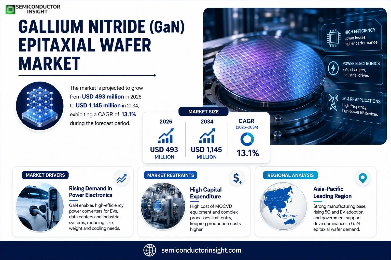
Gallium Nitride (GaN) Epitaxial Wafer market measured USD 493 million in 2026 and will climb to USD 1,145 million by 2034, delivering a compound annual growth rate of 13.1% over the forecast horizon.
An epitaxial waferalso referred to as an epi‑wafer or epiwaferis a semiconductor substrate produced through epitaxial growth techniques. These wafers serve as the foundational platform for photonics, microelectronics, spintronics and photovoltaic applications, enabling high‑performance device architectures.The upward trajectory stems from expanding adoption of GaN in RF power amplifiers for telecommunications, increasing integration of GaN power modules in electric‑vehicle drivetrains, and rising investment in next‑generation display technologies. Moreover, government incentives targeting energy‑efficient power conversion bolster demand across North America and Asia‑Pacific regions.
MARKET DRIVERS
Rising Demand in Power Electronics
Gallium Nitride (GaN) Epitaxial Wafer Market is benefiting from a surge in high‑efficiency power converters used in electric‑vehicle drivetrains and data‑center power supplies. Engineers prize GaN for its superior voltage‑handling capability, which translates into lighter, more compact designs that meet strict automotive weight targets and reduce cooling requirements in server farms. This functional advantage is prompting OEMs to replace silicon‑based modules with GaN‑based solutions, creating a tangible pull on wafer volumes.
Advances in Substrate Technology
Recent breakthroughs in low‑defect silicon‑carbide (SiC) and bulk GaN substrates have narrowed the performance gap between prototype and production parts. The improved lattice match reduces dislocation densities, allowing manufacturers to achieve higher yields at lower defect rates. As these substrates become more affordable, the cost premium associated with GaN epitaxy is eroding, encouraging design teams to specify GaN wafers early in the product development cycle.
➤ Industry analysts note that every 10 % improvement in wafer yield can shave up to 15 % off the bill‑of‑materials for power modules, directly boosting the market’s commercial appeal.
Supply‑chain consolidation is another catalyst; a handful of vertically integrated players now control both epitaxy and wafer processing, streamlining hand‑offs and shortening lead times. This operational efficiency gives end‑users confidence that GaN wafers can be sourced reliably for high‑volume programmes, reinforcing the upward trajectory of the market.
MARKET CHALLENGES
Manufacturing Yield Constraints
Despite the technology’s merits, achieving consistent wafer yields remains a technical hurdle. Epitaxial growth on large‑diameter substrates often encounters intracrystalline stresses that manifest as crack formation during cooling. When yield drops below 70 %, the cost structure tilts unfavourably, prompting some designers to revert to mature silicon alternatives for price‑sensitive applications.
Other Challenges
Material Uniformity
Uniform thickness and doping across a 200 mm wafer are critical for radio‑frequency (RF) and power‑device performance. Variations of even a few nanometres can cause frequency drift in RF front‑ends or premature breakdown in power transistors, forcing customers to impose stricter acceptance criteria that further strain production capacity.
MARKET RESTRAINTS
High Capital Expenditure
Establishing a state‑of‑the‑art MOCVD (metal‑organic chemical vapor deposition) line capable of delivering 150 mm and larger GaN wafers demands investment exceeding $150 million. The financial barrier limits entry to a few well‑funded incumbents, reducing competitive pressure on pricing and slowing the diffusion of newer process technologies into the broader market.
MARKET OPPORTUNITIES
Emerging 5G Infrastructure
5G base‑station arrays rely on high‑frequency, high‑power amplifiers where GaN’s electron‑mobility advantage yields superior output power density. Deployments across urban and rural sites are expected to raise the demand for RF‑grade GaN epitaxial wafers, especially in the 24 GHz to 40 GHz bands. Companies that can scale production while guaranteeing low‑phase‑noise characteristics are poised to capture a sizable share of this expanding segment.
Gallium Nitride (GaN) Epitaxial Wafer Market Trends
Rising Adoption in Power Conversion
The efficiency advantage of GaN epitaxial wafers is prompting OEMs to replace silicon‑based power modules in automotive chargers, data‑center adapters, and industrial drives. By delivering lower on‑resistance and faster switching, GaN devices cut energy loss and reduce thermal management costs, a combination that aligns with tighter emissions regulations and the price pressure on electric‑vehicle supply chains. As tier‑one manufacturers qualify GaN chips for series production, tier‑2 suppliers are expanding capacity to meet the anticipated order flow, creating a feedback loop that shortens lead times and stabilises pricing. This dynamic encourages new entrants to invest in scalable epitaxy reactors, reshaping the competitive landscape toward volume‑oriented players rather than niche specialists.
Other Trends
Shift Toward GaN‑on‑Silicon Platforms
Cost considerations are steering a sizable portion of the market toward GaN‑on‑silicon (GaN‑on‑Si) substrates. Silicon wafers benefit from mature fab infrastructure, enabling higher throughput and lower per‑unit expense compared with sapphire or silicon‑carbide alternatives. Manufacturers exploiting this platform can tap into existing silicon‑process lines, reducing capital outlay and shortening time‑to‑market for power and RF products. However, the thermal conductivity gap forces designers to adopt inventive heat‑spreading techniques, sparking a wave of packaging innovation. Companies that master this balance are positioned to capture mid‑range applications where price sensitivity outweighs the utmost performance demands.
Expansion of RF Device Applications
Wireless infrastructure upgrades for 5G, satellite broadband, and radar systems are widening the addressable market for GaN RF epitaxial wafers. The material’s high electron mobility and breakdown voltage enable power‑amplifier designs that operate at higher frequencies with superior linearity, a requirement for dense spectrum deployment. Service providers are prioritising base‑station upgrades that can handle larger bandwidths while maintaining energy efficiency, prompting chipset makers to integrate GaN solutions across front‑end modules. This trend is prompting downstream firms to re‑evaluate inventory strategies, as the lead time for GaN RF wafers remains tighter than for traditional compounds. Suppliers that can guarantee consistent wafer quality and rapid delivery are likely to secure long‑term contracts with telecom equipment vendors.
COMPETITIVE LANDSCAPEKey Industry Players
Gallium Nitride (GaN) Epitaxial Wafer Market – Competitive Overview
Sumitomo Electric Industries commands the upper tier of the GaN epitaxial wafer arena through a vertically integrated model that couples substrate preparation, metal‑organic chemical vapor deposition (MOCVD) capacity, and downstream packaging within a single corporate umbrella. Its large‑scale reactors, located in Japan and China, deliver consistent high‑quality GaN‑on‑SiC and GaN‑on‑Sapphire products that satisfy the stringent yield requirements of RF power amplifiers and power‑conversion modules. The firm’s strategic acquisitions of niche equipment vendors over the past three years have tightened its control over critical process steps, allowing it to out‑price emerging rivals while preserving margin stability. This concentration of capability forces smaller manufacturers to specialize in either thin‑film niche applications or customer‑specific customization, reinforcing a tiered market structure where one or two majors dictate price benchmarks and technology road‑maps.Beyond the dominant player, a constellation of specialists injects diversity into the supply chain. Mitsubishi Chemical Holdings leverages its extensive chemical‑process expertise to supply GaN‑on‑Si substrates aimed at automotive‑grade power devices, while Kyma Technologies differentiates with low‑defect‑density GaN‑on‑GaN wafers tailored for high‑frequency photonics. II‑VI Incorporated and Cree / Wolfspeed (a subsidiary of Wolfspeed) focus on high‑power RF platforms, emphasizing thermal management innovations. European entrants such as Infineon and NXP concentrate on integrating GaN epitaxy into mixed‑signal SoCs, positioning themselves for system‑level wins. Asian challengersincluding Skyworks Solutions, Qorvo, and Asian Semiconductor Manufacturing International Corp (ASMI)pursue aggressive capacity expansions to serve burgeoning 5G and data‑center markets. Meanwhile, boutique firms like HexaTech, Enkris, and Episil‑Precision secure contracts for custom epitaxial designs, serving niche sensor and spintronic applications that larger firms overlook. This blend of scale, regional focus, and technology specialization creates a competitive mosaic where collaboration and selective rivalry coexist.
List of Key Gallium Nitride (GaN) Epitaxial Wafer Companies Profiled
- Sumitomo Electric Industries
- Mitsubishi Chemical Holdings
- Kyma Technologies
- II‑VI Incorporated
- Cree / Wolfspeed
- Infineon Technologies
- NXP Semiconductors
- Skyworks Solutions
- Qorvo
- Asian Semiconductor Manufacturing International Corp (ASMI)
- HexaTech
- Enkris
- Episil‑Precision
- Seen Semiconductor
- Sinonitride
Segment Analysis:
| Segment Category | Sub-Segments | Key Insights |
| By Type |
|
GaN‑on‑Si
|
| By Application |
|
Power Electronics
|
| By End User |
|
Automotive
|
| By Growth Method |
|
MOCVD
|
| By Market Driver |
|
Energy Efficiency
|
Regional Analysis: Gallium Nitride (GaN) Epitaxial Wafer Market
North America
Canada’s contribution, though smaller in volume, adds a nuanced dimension through its emphasis on aerospace and defense applications, where reliability under extreme conditions is non‑negotiable. Collaborative programmes between federal research labs and private start‑ups are creating a pipeline of proprietary epitaxial growth techniques that could lower defect densities, a critical parameter for high‑frequency communication components.
The concentration of design‑win opportunities in automotive electrification, data‑center power supplies, and 5G radio frequency front‑ends is reshaping the procurement landscape. Suppliers that can guarantee consistent wafer thickness and crystal orientation are securing long‑term contracts, while those that lag in process repeatability face margin pressure. Consequently, the regional competitive balance is tilting toward firms that couple advanced MOCVD tooling with robust quality‑control analytics, a combination that is redefining the value chain across the continent.
Leading fabs are integrating low‑temperature epitaxy recipes that align with existing silicon‑on‑insulator lines, enabling hybrid platforms without extensive retooling. This convergence reduces capital outlay while delivering the performance edge that next‑generation power modules demand.
A tightly knit supplier base, anchored by a handful of specialty gas manufacturers, has established redundant logistics routes to mitigate disruptions. The emphasis on regional sourcing is sharpening as OEMs seek to shorten lead times for critical wafer batches.
Recent amendments to export‑control statutes have introduced clearer licensing pathways for high‑performance semiconductor equipment, fostering cross‑border collaborations while preserving national security safeguards.
Players that pair proprietary wafer‑scale epitaxy with in‑house metrology are differentiating themselves, capturing premium pricing tiers and reinforcing their status as preferred suppliers for mission‑critical projects.
Europe
European manufacturers are leveraging the region’s strong emphasis on sustainability to embed GaN wafers within renewable‑energy converters. German engineering firms, in particular, are aligning wafer specifications with grid‑stability standards, allowing higher inverter efficiencies. Meanwhile, the UK’s research institutions are piloting low‑defect growth chambers that could lower entry barriers for small‑scale producers. The convergence of policy incentives and academic expertise is fostering a collaborative ecosystem where design firms and material suppliers co‑develop application‑specific solutions, gradually shifting the market from a purely component focus to system‑level integration.
Asia‑Pacific
In Asia‑Pacific, a blend of aggressive capacity expansion and cost‑competitiveness defines market dynamics. Chinese fabs are scaling epitaxial lines to meet domestic demand for electric‑vehicle chargers, while Japanese corporations are concentrating on high‑frequency RF modules for 5G rollout. South Korea’s semiconductor conglomerates are integrating GaN wafers into power‑amplifier portfolios, capitalising on their heritage in wireless infrastructure. The regional narrative is shaped by governmental programmes that subsidise advanced material research, creating a pipeline of talent that supports both volume production and niche high‑performance applications.
South America
South American interest revolves around rugged power solutions for mining and remote‑grid operations. Brazil’s emerging semiconductor clusters are experimenting with GaN epitaxy to replace legacy silicon devices, attracted by the material’s ability to operate at higher temperatures with reduced cooling requirements. Local partnerships with North American equipment vendors are accelerating technology transfer, while regional trade agreements are easing access to critical precursors, gradually building a modest but strategically important market segment.
Middle East & Africa
The Middle East & Africa region is witnessing nascent adoption driven by telecom expansion and solar‑energy projects. United Arab Emirates’ smart‑city initiatives call for compact, high‑efficiency power converters, prompting early trials of GaN‑based modules. In Africa, pilot programs in off‑grid electrification are testing GaN wafers within micro‑grid inverters, seeking to reduce footprint and improve reliability in harsh climatic conditions. Although volume remains limited, the strategic focus on resilient power infrastructure is laying groundwork for future growth.
Report Scope
This market research report provides a comprehensive analysis of the Gallium Nitride (GaN) Epitaxial Wafer Market , covering the forecast period 2026–2034. It offers detailed insights into market dynamics, technological advancements, competitive landscape, and key trends shaping the industry.
Key focus areas of the report include:
- Market Overview: The report begins with an overview outlining its current market scenario, key growth indicators, and industry transformation drivers. It discusses macroeconomic factors, demand–supply balance, regulatory landscape, and the strategic role of semiconductors in powering advancements across industries such as automotive, telecommunications, consumer electronics, and industrial automation.
- Market Size & Forecast: Historical data and future projections for revenue, unit shipments, and market value across major regions and segments.
- Segmentation Analysis: Detailed breakdown by product type, technology, application, and end-user industry to identify high-growth segments and investment opportunities.
- Regional Insights: Insights into market performance across North America, Europe, Asia-Pacific, Latin America, and the Middle East & Africa, including country-level analysis where relevant.
- Competitive Landscape: Profiles of leading market participants, including their product offerings, R&D focus, manufacturing capacity, pricing strategies, and recent developments such as mergers, acquisitions, and partnerships.
- Technology Trends & Innovation: Assessment of emerging technologies, integration of AI/IoT, semiconductor design trends, fabrication techniques, and evolving industry standards.
- Market Drivers & Restraints: Evaluation of factors driving market growth along with challenges, supply chain constraints, regulatory issues, and market-entry barriers.
- Stakeholder Insights: Insights for component suppliers, OEMs, system integrators, investors, and policymakers regarding the evolving ecosystem and strategic opportunities.
Primary and secondary research methods are employed, including interviews with industry experts, data from verified sources, and real-time market intelligence to ensure the accuracy and reliability of the insights presented.
FREQUENTLY ASKED QUESTIONS:
What is the current market size of Gallium Nitride (GaN) Epitaxial Wafer Market?
-> Gallium Nitride (GaN) Epitaxial Wafer Market was valued at USD 493 million in 2026 and is expected to reach USD 1145 million by 2034, at a CAGR of 13.1% during the forecast period.
Which key companies operate in Gallium Nitride (GaN) Epitaxial Wafer Market?
-> Key players include Sumitomo Electric Industries, Mitsubishi Chemical Holdings, Sumitomo Chemical, Kyma Technologies, HexaTech, Sinonitride, Enkris, Seen Semiconductor, and Episil-Precision.
What are the key growth drivers?
-> Key growth drivers include rise in 5G infrastructure, electric‑vehicle power systems, renewable‑energy conversion, and increasing demand for high‑efficiency RF and power devices.
Which region dominates the market?
-> Asia‑Pacific remains the largest market by revenue, although growth slowed in 2022, while North America and Europe also display strong demand.
What are the emerging trends?
-> Emerging trends include GaN‑on‑Si and GaN‑on‑SiC substrate development, integration of GaN in automotive power modules, and expansion of GaN applications in data‑center power supplies.
Get Sample Report PDF for Exclusive Insights
Report Sample Includes
- Table of Contents
- List of Tables & Figures
- Charts, Research Methodology, and more...
 Download Sample Report PDF