Key Statistics
Key Takeaways
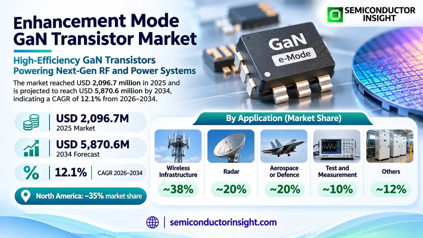
- Enhancement-mode GaN revenue is projected to increase from USD 2,096.7 million in 2025 to USD 5,870.6 million in 2034, a 12.1% CAGR. The forecast includes substrate and application categories spanning high-frequency and power-conversion semiconductor devices.
- GaN-on-SiC substrate has an estimated ~62% share according to the source segmentation, with GaN-on-Si comprising ~38%. Thermal performance and wafer economics influence choices across high-power radio-frequency and power-switching designs.
- Application pathways include wireless base-station electronics, radar transmitters, aerospace systems, specialist test benches and compact power conversion. Their transistor voltage, operating frequency and qualification requirements are markedly different, even though the active material is gallium nitride.
- North American demand has an estimated ~35% share, with Asia-Pacific ~32%, Europe ~22%, South America ~6% and Middle East & Africa ~5%. Supply chains combine semiconductor design, epitaxy, fabrication and system qualification.
- 2026 GaN activity includes Nexperia expanding low-voltage and 650 V devices, EPC entering 40 V Gen 7 eGaN volume production and Infineon announcing a future 300 mm wafer manufacturing programme in Austria.
Enhancement-mode GaN Transistor Market Overview
Enhancement-mode GaN transistor market reached USD 2,096.7 million in 2025 and is projected to reach USD 5,870.6 million in 2034, indicating a CAGR of 12.1% from 2026–2034. North America represents an estimated ~35% share, with activity spanning advanced power electronics and high-frequency infrastructure. Commercial evaluation depends on verified gate characteristics, packaging technology and application-specific reliability evidence instead of a generic wide-bandgap advantage.
Enhancement-mode gallium nitride devices are normally off at zero gate bias and require a suitable positive gate control to conduct. GaN high electron mobility transistors can exhibit low charge and fast switching, offering efficiency benefits in selected power stages. Their behavior differs from normally-on depletion-mode structures and from silicon MOSFETs. Designers must manage gate-voltage limits, switching loops, parasitic inductance and thermal pathways before a promising die becomes a qualified circuit component.
The revenue boundary follows the enhancement-mode transistor product group described by the source, covering GaN-on-SiC and GaN-on-Si substrate categories across wireless infrastructure, radar, defence, test equipment and other systems. It excludes complete telecommunications base stations, electric vehicles, radar assemblies and finished power supplies. Some RF GaN-on-SiC amplifiers use related materials but are not necessarily normally-off devices; where enhancement behavior is unverified, their specifications are engineering context rather than proof of direct merchant e-mode shipments.
GaN-on-SiC offers strong thermal conductivity and is widely used in demanding high-frequency equipment, whereas GaN-on-Si can benefit from the scale and cost infrastructure of larger silicon wafer processing. At the circuit level, a 40 V eGaN power transistor serves a very different function from a 650 V charging converter switch or a 2.4 GHz RF amplifier. Substrate, gate structure and package all affect what part a customer can actually substitute into a system.
Commercialization depends on repeatable dynamic on-resistance, gate stability, avalanche or surge behavior, thermal resistance and realistic high-frequency switching. Infineon has described a 300 mm GaN power wafer manufacturing plan, while current vendors supply 650 V and 700 V products and lower-voltage devices. A capacity announcement should not be equated with operating annual chip output before the associated facility reaches production. Application engineering and design-in qualification remain important adoption barriers.
Segment Analysis: By Type
GaN-on-SiC represents an estimated ~62% of the substrate-type value described for enhancement-mode GaN transistors, while GaN-on-Si represents about ~38%. The former combines GaN active layers with a thermally conductive SiC foundation, valuable in demanding high-frequency contexts. The latter uses a silicon base that can support cost-competitive scaled processing. Actual gate and channel constructions differ across vendors, so substrate classification alone does not establish normally-off behavior.
| Type | Function | Market position |
|---|---|---|
| GaN on SiC | GaN epitaxial layers on silicon carbide provide strong heat-spreading potential and enable high-power radio-frequency transistor architectures. Wireless infrastructure and radar can demand substantial power density over frequency bands measured in GHz. MACOM lists products built with GaN-on-SiC for demanding RF amplifiers, but a purchaser must confirm the gate structure and normally-off operating mode before classifying an individual device as enhancement-mode. | Largest substrate type, estimated ~62% share, ~11.6% CAGR. Thermally demanding RF and aerospace equipment contributes to this category in the original market segmentation. Silicon-carbide substrate cost and epitaxial process control can be meaningful constraints. Qualification emphasizes RF reliability, thermal interfaces, device consistency and a physical package compatible with the actual amplifier circuit. |
| GaN on Si | GaN deposited on silicon supports power-electronic transistor structures using semiconductor fabrication infrastructure that can scale to comparatively large wafers. Normally-off power devices may be deployed in compact converters, DC-DC rails or fast-switching industrial circuits. Infineon, EPC and other suppliers document enhancement-mode options across different voltage ratings and form factors. The wafer base does not eliminate challenges in buffer stress, traps or dynamic device behavior. | Complementary substrate type, estimated ~38% share, ~13.0% CAGR. Demand is supported by energy-efficiency upgrades and design opportunities across 18 V to 700 V device families. Supplier capabilities differ in wafer size, die structure and integrated gate-drive protection. Customers select parts according to rated voltage, on-resistance, switching loss and operating environment rather than by substrate price alone. |
Secondary segmentation: Voltage Range
The enhancement-mode GaN transistor market also distinguishes devices rated below 200 V, at 200–600 V and above 600 V. These categories map to different converter topologies and customer priorities rather than a universal quality ranking. Low-voltage devices can target synchronous rectification or DC-DC rails, mid-voltage products address specialized power stages, and high-voltage parts can serve offline AC-DC and industrial power systems. Estimated shares sum to the same transistor revenue viewed by voltage rating.
| Axis | Members | Commercial role |
|---|---|---|
| Voltage Range | Below 200V; 200-600V; Above 600V | Lower voltage switching emphasizes very low resistance and gate charge, while higher voltage ratings make blocking capability, thermal design and board isolation increasingly important. The categories are independent of substrate and application classification. The device may also be integrated with a gate driver, but that package arrangement is separate from the electrical voltage classification and has its own qualification requirements. |
| End-use fit | Compact conversion; industrial supplies; selected high-power infrastructure | A 40 V EPC device is not interchangeable with an Infineon 650 V transistor, even when both use normally-off GaN principles. Rated voltage and gate driver design must match the circuit, cooling requirements and compliance environment. Designers also examine the effect of repetitive turn-off transients and temperature on allowable operating margin, rather than relying only on the nominal maximum blocking voltage. |
Segment Analysis: By Application
Wireless infrastructure is the largest application at an estimated ~38% share, while radar and aerospace or defence each contribute roughly ~20%. Test and measurement systems account for ~10%, and other power-electronic or industrial functions add ~12%. These application labels reflect different device requirements: radio-frequency performance may drive one purchase, while low conduction and switching loss drive another.
| Application | Demand characteristics |
|---|---|
| Wireless Infrastructure | Largest application, estimated ~38% share, ~11.7% CAGR. Mobile infrastructure relies on efficient RF signal amplification across several frequency bands, and the source associates GaN with high-density 5G power stages. GaN-on-SiC technology is important in this context, but conventional RF amplifier products should not automatically be described as normally-off. Equipment builders qualify transistor frequency response, efficiency, power linearity, cooling and long-term reliability. |
| Radar | Radar systems, estimated ~20% share, ~12.8% CAGR. High-frequency radar architectures can benefit from GaN power density and thermal capability where semiconductor technology matches the amplifier requirements. Radar frequency, output waveform and pulsed duty cycle affect device selection. The complete radar equipment price is not transistor revenue. RF product listings may illustrate use cases even when enhancement-mode status needs separate device-level confirmation. |
| Aerospace & Defence | Specialized systems, estimated ~20% share, ~11.6% CAGR. Defence communications and airborne electronics require careful thermal, reliability and lifecycle validation. A GaN transistor’s value depends on tested performance at the intended voltage and frequency, not simply the material used for its epitaxial layers. Qualification may consider wide environmental ranges, radiation-related constraints where relevant and repeatable RF or switching behavior throughout a system service life. |
| Test & Measurement | Instrumentation, estimated ~10% share, ~11.3% CAGR. Semiconductor measurement platforms and RF laboratory equipment use specialized power and signal devices, where repeatable operating conditions are essential. A characterization setup may evaluate 650 V blocking characteristics or GHz-range high-frequency amplifier behavior depending on the device. Test hardware supports design verification but is not interchangeable with the transistor product sold into production converters. |
| Others | Additional applications, estimated ~12% share, ~13.8% CAGR. Compact power supplies, DC-DC conversion, robotics and selected charging products create opportunities for normally-off GaN switching. EPC announced a 40 V device intended for high-density power systems in 2026, and Nexperia expanded 18 V to 200 V offerings. These devices serve different operating conditions from radio-frequency GaN components, although both benefit from advances in materials and packaging. |
Application selection involves voltage, gate charge, operating frequency and failure behavior. A 2.3 GHz RF device driving communications infrastructure can dissipate heat very differently from a 650 V AC-DC switching transistor; a 40 V synchronous rectifier has a third set of optimization goals. The market’s application categories therefore describe commercial use rather than a common physical device architecture. Customers usually qualify the semiconductor in its actual switching or amplifier circuit before volume adoption.
Regional Analysis
North America is the leading enhancement-mode GaN market at an estimated ~35%, followed by Asia-Pacific ~32%, Europe ~22%, South America ~6% and the Middle East & Africa ~5%. Regional demand reflects power electronics design, high-frequency systems and semiconductor manufacturing investment. The manufacturing site of a GaN wafer is not necessarily the location where the final converted-power equipment is used.
Which regions lead enhancement-mode GaN demand and commercialization?
United States engineering supports low-voltage eGaN developments and high-frequency equipment, while Asian electronics production creates important scale opportunities. Europe hosts power semiconductor firms and planned new wafer investments, including Infineon’s 300 mm announcement. Emerging regions demand efficient infrastructure systems without necessarily producing the transistor wafers locally. Supplier ownership, device technology and the distinction between proposed production and actual manufacturing matter for a realistic competitive assessment.
| Region | Position | Growth outlook | Demand profile | What decides supplier selection |
|---|---|---|---|---|
| North America | Largest (~35%) | ~11.1% CAGR | RF infrastructure, semiconductor design and power systems | |
| Asia-Pacific | Strong (~32%) | ~13.2% CAGR | Wafer manufacturing, electronics and power conversion | |
| Europe | Strong (~22%) | ~11.9% CAGR | Power conversion, specialty chips and fabrication plans | |
| South America | Developing (~6%) | ~12.3% CAGR | Industrial supply, communications and energy projects | |
| Middle East & Africa | Developing (~5%) | ~12.5% CAGR | Industrial resilience and specialized RF power |
Key Enhancement-mode GaN Transistor Manufacturers and Competitive Landscape
Competition spans companies with verified enhancement-mode GaN power devices and other firms active in wider GaN radio-frequency technology. Infineon owns the former GaN Systems business after its October 2023 acquisition. Efficient Power Conversion, Nexperia, STMicroelectronics and Texas Instruments have documented power conversion parts; RF GaN vendors including MACOM participate in adjacent high-frequency technology that requires careful device-level scope verification.
Infineon markets CoolGaN transistor families in 650 V and 700 V classes and announced a future 300 mm European GaN wafer plant in October 2026. GaN Systems became part of Infineon in 2023 and is not an independently operating current rival. The combined business has several power-device options and application support activities. A future wafer facility signals investment intention, not automatically new revenue from already manufactured transistor inventory.
Efficient Power Conversion introduced the EPC2366 seventh-generation 40 V eGaN transistor into volume production in 2026, emphasizing low on-resistance and strong performance in compact DC-DC systems. Nexperia extended high-power 650 V devices in June 2026 and 18–200 V products in November. STMicroelectronics supplies integrated MASTERGAN devices containing normally-off transistors and gate drivers, while Texas Instruments provides integrated GaN stages with sensing or protection. These businesses serve different voltage and package needs.
NXP Semiconductors, Qorvo, Microchip and MACOM appear in the broader company universe. In RF markets, GaN-on-SiC can offer substantial thermal advantages, but a published high-power amplifier specification does not by itself identify the transistor as normally-off. VisIC Technologies is associated with GaN power-device technology. Qualification, wafer sourcing and the separation of standalone transistor value from integrated modules are essential when comparing commercial positions.
Tier structure
| Tier | Companies | Basis of competition |
|---|---|---|
| Normally-off power GaN | Infineon; Efficient Power Conversion; Nexperia | These suppliers publicly document discrete enhancement-mode power transistors across low and high voltage classes. They compete on resistance, charge, gate ruggedness and appropriate packages as well as production continuity and application support. An engineering support ecosystem can influence adoption when small differences in gate impedance or packaging significantly change measured converter performance. |
| Integrated GaN power stages | STMicroelectronics; Texas Instruments | Integration combines normally-off GaN silicon or compound semiconductor functions with specialized drivers and protective circuitry. The assembly value differs from a bare transistor and creates a distinctive alternative for designers who want fewer external parts. Integrated solutions require evaluation as a complete assembly; their sales cannot automatically be divided into identical shares for each individual internal device. |
| RF and technology ecosystem | MACOM; Qorvo; NXP Semiconductors; Microchip; VisIC Technologies | GaN-on-SiC RF offerings illustrate adjacent high-frequency demand, while emerging device developers can contribute innovation. A product must be confirmed normally-off before its full sale is treated as part of the title market; company presence in GaN alone is insufficient. Frequency band, output linearity and thermal behavior must all be verified before an RF component is considered comparable with a normally-off converter transistor. |
Key companies profiled
- Infineon Technologies (GaN Systems acquired 2023)
- Efficient Power Conversion
- Nexperia
- STMicroelectronics
- Texas Instruments
- VisIC Technologies
- MACOM (RF GaN technology)
- Qorvo
- NXP Semiconductors
Enhancement-mode GaN Transistor Production Capacity Analysis
Enhancement-mode GaN production starts with suitable substrates and epitaxial growth, followed by device processing, passivation, metallization and careful assembly into low-inductance packages. Dynamic reliability is particularly important because traps, interfaces and gate design can affect actual on-state resistance at high switching rates. Qualification differs for an RF GaN-on-SiC structure, a discrete e-mode GaN-on-silicon transistor and an integrated power stage.
Substrate and epitaxy processes determine crystalline quality and dislocation behavior. GaN-on-SiC places the active semiconductor above a thermally capable silicon carbide substrate, while GaN-on-silicon involves managing strain and electrical isolation on silicon wafers. A 200 mm power process and a proposed 300 mm operation need different equipment scale, yield control and investment. Wafer count alone does not establish how many fully qualified enhancement-mode devices reach customers.
Gate structure and passivation shape the stability of normally-off operation. A transistor rated 650 V may have strict recommended gate-drive voltage and switching transient limits. Process engineering measures dynamic resistance, gate leakage and thermal performance as well as static wafer probe properties. Production tests therefore combine die screening with package-level electrical and reliability validation. A high-performance laboratory demonstration is not equivalent to a released commercial product.
Packaging affects parasitic inductance and heat extraction in fast GaN circuits. EPC describes a 3.3 × 2.6 mm package for a 40 V device, while Nexperia offers TO-247, TOLL and TOLT options around 650 V. Integrated GaN half-bridges combine 2 switches and a gate driver in a separate product class. Manufacturing capacity includes device fabrication, assembly and test capability and must be assessed using operating lines rather than only construction plans.
Enhancement-mode GaN Transistor Market Dynamics: Drivers, Restraints and Opportunities
The expansion of normally-off GaN devices is supported by efficiency, fast switching and high-frequency system development, while adoption is limited by advanced fabrication costs and demanding gate-drive qualification. Different device classes face different price and reliability constraints. The following impact analysis reflects the contributions of technology and demand factors to the headline forecast rate.
MARKET DRIVERS
Drivers Impact Analysis*
| Market Drivers | Impact Rank | CAGR Contribution (%) | 2026–2028 | 2029–2031 | 2032–2034 |
|---|---|---|---|---|---|
| High-efficiency power conversion | High | +7.00% | High | High | High |
| Wireless and RF infrastructure | Medium-High | +4.50% | High | High | High |
| GaN device manufacturing scale | Medium | +3.30% | Medium | High | High |
| Electric vehicle power systems | Low-Medium | +2.20% | Medium | High | High |
| Others (new specialist designs) | Low | +1.00% | Low | Medium | Medium |
Power-density opportunities broaden GaN applications
Normally-off GaN switches can enable rapid switching in compact DC-DC and AC-DC circuits. Low gate charge and suitable on-resistance may reduce losses where a designer carefully controls loop inductance. An EPC 40 V product and an Infineon 650 V part therefore address different power stages. Adoption follows successful converter qualification, not just a data sheet claim that the wide-bandgap material can switch quickly.
Telecom and RF needs support specialized transistor structures
Wireless infrastructure requires efficient radio frequency output stages and improved thermal control. GaN-on-SiC is associated with high-frequency high-power amplifiers, and MACOM documents products in multiple GHz bands. A radio system can use GaN materials while still requiring proof of enhancement-mode gate operation for a particular transistor. Spectrum requirements, linearity and thermal design determine the commercial opportunity for a qualified product.
Maturing wafer production improves supplier options
Infineon announced planned 300 mm GaN power semiconductor manufacturing at Villach in October 2026, reflecting ambitions for scale. Nexperia launched new 650 V and low-voltage families in the same year, while EPC reported a new generation moving into volume output. Greater availability could support larger design programmes, but real supply capacity requires established process yield, package availability and qualified manufacturing data.
MARKET RESTRAINTS
Restraints Impact Analysis*
| Market Restraints | Impact Rank | CAGR Contribution (%) | 2026–2028 | 2029–2031 | 2032–2034 |
|---|---|---|---|---|---|
| Substrate and fabrication premium | High | -2.80% | High | Medium | Medium |
| Gate drive and reliability challenges | Medium-High | -1.70% | High | High | Medium |
| Package thermal and EMI constraints | Medium | -0.90% | High | Medium | Medium |
| Others (qualified supply competition) | Low | -0.50% | Medium | Low | Low |
Wide-bandgap manufacturing can cost more
Substrates, epitaxy and precision process control contribute to unit economics, particularly for demanding high-frequency or high-voltage devices. A GaN transistor may provide a smaller converter but still carry a price or test premium compared with a mature silicon alternative. Customers evaluate the entire bill of materials, including gate drivers and cooling. Substitution is less attractive when a conventional silicon MOSFET already meets efficiency and space requirements.
Gate stability and switching design complicate adoption
Enhancement-mode GaN devices demand gate bias control and minimized parasitic inductance because very rapid transitions can create overvoltage or ringing. A 650 V part needs a different layout and insulation design from a 40 V device. Dynamic resistance and thermal transient behavior can complicate qualification. Designers without suitable power-electronics expertise may choose a more familiar switch even where GaN offers theoretical performance benefits.
Thermal and interference requirements remain strict
High-frequency switching can reduce some losses but also generate electrical noise that requires control in layout and filtering. RF products face different linearity and thermal stability constraints. Package design, heatsinking and environmental conditions affect achievable reliability. A device showing excellent bench efficiency at moderate temperature may require more careful derating at a severe industrial ambient. These system-level considerations can delay new production designs.
MARKET OPPORTUNITIES
New low-voltage e-mode devices
EPC moved a seventh-generation 40 V GaN transistor to mass production in January 2026, while Nexperia announced 18–200 V devices in November. These parts expand the range of practical low-voltage conversion projects. A 0.32 mΩ device can target a different current and packaging profile from a 140 mΩ high-voltage switch. Designers still compare system efficiency and cooling requirements under realistic conditions.
European larger-wafer power fabrication
Infineon described a 300 mm wafer plan in Austria, with commercial ramp depending on market development. Larger wafers could enable more devices per substrate when quality and yield are adequate. Packaging, wafer test and customer qualification must scale with fabrication to realize cost benefits. The investment also strengthens regional power-semiconductor engineering capacity, although potential future capacity cannot be treated as already delivered market revenue.
Converter integration and gate-driver simplification
STMicroelectronics MASTERGAN6 contains a pair of 650 V enhancement-mode transistors plus a high-voltage gate driver. Integrated protection can reduce the number of external control components and simplify part of the engineering effort. A supplier can win applications where the customer values practical integration over the lowest die price. The complete circuit still needs electrical isolation, EMI testing and thermal analysis for its intended operating conditions.
Selective high-frequency infrastructure upgrades
Thermally robust GaN-on-SiC technology continues to serve specialized RF power amplification in wireless, radar and other equipment. Data sheets citing 2.3–2.4 GHz and 4.9–5.0 GHz operating bands illustrate different market needs. Adoption of enhancement-mode designs within such systems depends on a confirmed normally-off technology and system validation. High-frequency material benefits alone do not guarantee a particular type of gate or commercial part.
Enhancement-mode GaN Transistor Supply Chain Analysis
The GaN transistor value chain combines substrate supply, epitaxial deposition, device fabrication, packaging and customer qualification. Power-electronics integrators then build switching circuits with drivers, magnetic components and thermal management, while RF manufacturers evaluate amplifier performance and stability. Every stage affects yields and reliability. Announcements of new factories concern future upstream capacity and should not be conflated with sales from delivered transistor devices.
Substrate sourcing and epitaxial layers. High-quality GaN crystal formation is a foundation of reliable power devices. GaN-on-SiC leverages heat-spreading potential but can face expensive substrate costs, while GaN-on-silicon must control strain and buffer leakage. The production process includes material inspection, epi thickness measurement and electrical tests. A 200 mm wafer capability can lower some scaling hurdles, but the eventual number of accepted dies still depends on defects and qualified device geometry.
Gate processing and normally-off control. Enhancement-mode operation depends on an effective normally-off structure whose gate threshold stays within a useful range. Fabricators control dielectric or p-GaN processes, contacts, defect states and surface passivation. Devices are tested for static leakage, switching charge and behavior under stress. A 650 V blocking rating does not describe the full gate-drive specification, and each product requires circuit guidance to prevent overdrive or false turn-on during rapid transitions.
Packaging and thermal qualification. Fast power devices can lose theoretical advantages when package inductance or poor heat paths create excess loss. Customers compare 9 × 9 mm integrated modules, compact EPC packages and larger TO-247 style high-power packages according to system needs. Packaging tests may involve thermal cycling and high-temperature operation. Qualified assembly capacity is therefore a material part of the effective supply chain, not merely a finishing service for already valuable wafers.
Converter and amplifier manufacturing. Equipment integrators attach selected GaN devices to gate drivers, PCBs, filters, magnetics and heat sinks. A 40 V server rail and a 650 V industrial switch need distinct safety and electrical arrangements. RF amplifiers require impedance matching and high-frequency measurements in addition to thermal control. An integrated finished power converter contains many parts whose value is outside the transistor product definition, even though system adoption influences device demand.
Recent Developments in the Enhancement-mode GaN Transistor Market
- 10 November 2026 Low-voltage device portfolio
Nexperia announced GaN transistors covering 18 V through 200 V with on-resistance down to 0.32 mΩ, targeting robotics, AI hardware and power conversion. The release broadens the low-voltage choices available for compact, fast-switching architectures. Production qualification and thermal capability remain specific to each device. These transistor specifications should not be interpreted as shipments of the downstream equipment or confirmation of every planned system design. Source - 27 October 2026 Planned 300 mm GaN manufacturing
Infineon announced a planned high-volume gallium nitride power semiconductor facility for 300 mm wafers at Villach in Austria, with investment of approximately €1.1 billion. The plan aims to support future production at increased wafer scale. This is a dated capital and capacity initiative, not evidence that a full commercial 300 mm line had already completed its production ramp during 2026. Its relevance is supply-chain development. Source - 10 June 2026 High-voltage device expansion
Nexperia expanded its 650 V GaN device portfolio with 35, 50 and 70 mΩ on-resistance options in multiple packages. These choices can help converter engineers balance operating losses, space and heat extraction, subject to board-level validation. The announcement concerns high-power product availability rather than the value of finished renewable-energy installations. Different GaN families also have different gate architectures, so part-level qualification remains necessary. Source - 30 January 2026 Seventh-generation eGaN production
Efficient Power Conversion announced volume production of the EPC2366, a 40 V enhancement-mode transistor with typical 0.84 mΩ on-state resistance. The device is designed for dense high-current power stages and offers compact packaging. Successful implementation depends on the actual drain voltage, thermal conditions and switching waveform. The release demonstrates manufacturing progress in low-voltage GaN without implying that all GaN transistor types share the same electrical design. Source - 10 November 2025 Integrated GaN package qualification
STMicroelectronics listed a November 2025 specification revision for the MASTERGAN6 650 V integrated half-bridge, which contains two enhancement-mode transistors and a dedicated driver. The part illustrates the movement toward integration of switching silicon alternatives and application control. Its price includes more than bare GaN transistors, making system-in-package content a distinct competitive consideration. Final equipment still requires power, safety and thermal qualification. Source
REPORT SCOPE & SEGMENTATION
| Attribute | Details |
|---|---|
| Study Period | 2020–2034 |
| Base Year | 2025 |
| Estimated Year | 2026 |
| Forecast Period | 2026–2034 |
| Historical Period | 2020–2024 |
| Market Size 2025 | USD 2,096.7 million |
| Market Size 2026 | USD 2,350.8 million |
| Market Size 2034 | USD 5,870.6 million |
| Growth Rate | CAGR of 12.1% during 2026–2034 |
| Unit | Value in USD million for enhancement-mode GaN transistor devices |
| Segmentation | By Type, Application, Voltage Range and Global Region |
| By Type | GaN on SiC; GaN on Si |
| By Application | Wireless Infrastructure; Radar; Aerospace & Defence; Test & Measurement; Others |
| By Voltage Range | Below 200V; 200-600V; Above 600V |
| By Region | Global market across North America, Asia-Pacific, Europe, South America and Middle East & Africa with country examples from the U.S., China, Germany, Brazil and Saudi Arabia. North AmericaUnited States, Canada, Mexico Asia-PacificChina, Japan, South Korea EuropeGermany, France, United Kingdom South AmericaBrazil, Chile, Argentina Middle East & AfricaUnited Arab Emirates, Saudi Arabia, South Africa |
| Key Companies Profiled | Infineon Technologies (including acquired GaN Systems); Efficient Power Conversion; Nexperia; STMicroelectronics; Texas Instruments; VisIC Technologies; NXP Semiconductors; Qorvo; Microchip Technology; MACOM (RF adjacent) |
| Customization Scope | Study includes substrate-related production, voltage classes, normally-off GaN power devices, selected RF applications, wafer development, manufacturer ownership and circuit qualification. |
Frequently Asked Questions
How large is the enhancement-mode GaN transistor market?
Global enhancement-mode GaN transistor value is estimated at USD 2,096.7 million in 2025 and forecast at USD 5,870.6 million in 2034, a CAGR of 12.1% during 2026–2034. The market covers named substrate and application classes of transistor devices, not the full sales value of telecommunications, charging or industrial equipment. The forecast depends on continuing device qualification and manufacturing development.
What makes a GaN device enhancement-mode?
Enhancement-mode GaN devices are normally off when the gate is not driven to an appropriate positive control potential. They may provide low charge and rapid switching for demanding power circuits. The relevant gate threshold and safe voltage range vary by part and technology, so a driver must match the selected die. Not every GaN-on-SiC radio-frequency amplifier automatically uses the same normally-off construction.
Which substrate category leads the market?
GaN-on-SiC carries an estimated ~62% share in the source classification, compared with ~38% for GaN-on-silicon. SiC can provide advantageous thermal conductivity for demanding high-frequency functions, while silicon wafer processing may offer important scale benefits for certain power devices. These classifications do not independently establish the gate mode of each commercial component. The vendor’s detailed part specification remains essential.
What is the largest application segment?
Wireless infrastructure represents an estimated ~38% share of the market, reflecting the relevance of GaN technology to high-power RF equipment. Radar and aerospace or defence each contribute around ~20%, followed by test and measurement ~10% and other systems ~12%. A transistor supplying a radio-frequency stage should be distinguished from the full amplifier or antenna product. Design wins depend on frequency, linearity, temperature and qualification.
Which region leads demand?
North America has an estimated ~35% share, with Asia-Pacific near ~32% and Europe around ~22%. The United States supports specialty semiconductor design and power electronics development, while Asian assembly and wafer activity influence broader manufacturing. Europe is developing additional GaN fabrication capacity plans. The location of a semiconductor company’s headquarters may differ from the wafer plant or equipment customer market.
How do voltage classes differ?
Below-200 V GaN devices may serve compact conversion and synchronous rectification, while 200–600 V classes address other intermediate power designs. Above-600 V products are relevant to some offline supplies and industrial converters. Nexperia lists devices from 18 V to 700 V across its wider portfolio. Different voltage classes involve different gate drives, insulation and thermal design, so they are not interchangeable solely because both use GaN.
Which companies sell normally-off GaN devices?
Infineon sells CoolGaN families and owns the former GaN Systems company. EPC introduced a 40 V Gen 7 eGaN transistor in 2026, Nexperia lists low and high voltage devices, and ST and TI offer integrated power stages. RF GaN component firms also participate in relevant technology, but individual amplifier products require separate confirmation of their gate architecture. Commercial comparison depends on actual qualified part numbers.
What changed in GaN manufacturing during 2026?
Infineon announced a planned 300 mm GaN power semiconductor facility in Austria in October 2026. Nexperia widened its 650 V and low-voltage device portfolios, while EPC reported seventh-generation volume production. These milestones concern different parts of the supply chain. A proposed wafer facility does not contribute production volume until fabrication equipment, yield and customer qualification are operational.
Why can GaN transistor adoption be challenging?
High-frequency switching raises concerns over gate overshoot, electromagnetic interference, thermal behavior and dynamic resistance. GaN substrates and epitaxial processing can also cost more than mature silicon options, particularly when yields or test requirements are demanding. A fast switch needs appropriate PCB layout and driver control, and RF components have separate linearity considerations. Buyers compare complete system economics and reliability rather than relying on material properties alone.
Where are the major opportunities?
High-density DC-DC conversion, efficient industrial power supplies, selected RF infrastructure and specialized test systems offer distinct openings. A 40 V EPC eGaN device addresses different requirements from an Infineon 650 V transistor or a multi-GHz RF power amplifier. Improvements in packaging and future wafer scale can increase design options, but success depends on verified efficiency, production yield and long-term component availability.
Research Sources & Evidence Base
Get Sample Report PDF for Exclusive Insights
Report Sample Includes
- Table of Contents
- List of Tables & Figures
- Charts, Research Methodology, and more...
 Download Sample Report PDF