Key Statistics
Key Takeaways
- Market value: the organic light emitting transistor market is valued at USD 271.74 million for 2025, with an estimated USD 314.89 million in 2026 and a projected USD 1,023.84 million in 2034; its forecast reflects research-stage devices, engineering programmes and pilot commercial activity rather than proven mass-market OLET shipment counts.
- Device architecture: multilayer OLETs lead the modeled type mix at ~62% because separate charge-transport and emissive functions offer greater control over carrier injection, recombination location and spectral output, while single-layer approaches remain important for simplified and flexible fabrication.
- Application mix: consumer electronics accounts for a modeled ~35% of the base-year opportunity, although wearable visual indicators, interactive surfaces and near-eye components remain development prospects rather than confirmed high-volume transistor-emitter products.
- Regional position: Asia-Pacific represents an estimated ~44% of the market in 2025, reflecting active university and materials research in East Asia alongside an established organic-electronics supply ecosystem; the share is an analytical allocation, not a disclosed manufacturer sales figure.
- Growth constraints: device stability, inconsistent electroluminescence across a transistor channel, interface defects and competing mature OLED-plus-TFT assemblies create qualification hurdles that may delay commercialization even when laboratory efficiency improves.
Organic Light Emitting Transistor Market Overview
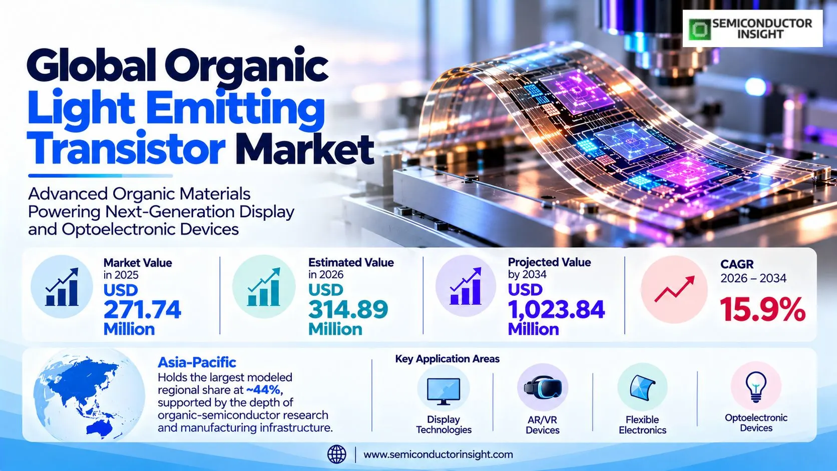
Organic light emitting transistor market was valued at USD 271.74 million in 2025, is estimated at USD 314.89 million in 2026, and is projected to reach USD 1,023.84 million by 2034, advancing at a CAGR of 15.9% during 2026–2034. Asia-Pacific holds the largest modeled regional share at ~44%, supported by the depth of organic-semiconductor research and manufacturing infrastructure.
An organic light-emitting transistor, or OLET, combines the electrical switching function of an organic transistor with light generation in the semiconductor channel. Unlike a conventional organic light-emitting diode panel that depends on a separate thin-film transistor to drive each pixel, the emissive transistor can control its own optical output through the gate electrode. This combination offers architectural possibilities for compact indicators, distributed light-emitting circuits and flexible electronic surfaces, but it introduces a difficult requirement: charge transport and radiative recombination must both perform efficiently in the same device.
The market boundary covers integrated light-emitting organic transistors, their saleable device assemblies and revenue associated with prototype, engineering and pilot production within the publisher-defined market. It does not include ordinary OLED panels driven by separate switching transistors, non-emissive organic field-effect transistors, standalone emitter chemicals or complete consumer devices. The distinction prevents mature OLED display revenue from being misidentified as OLET commercialization and keeps research programmes separate from established high-volume display supply chains.
Two engineering families shape the opportunity. Single-layer devices place switching and emission into a relatively simple active structure, which may reduce processing steps but complicates the simultaneous optimization of hole mobility, electron injection and exciton formation. Multilayer devices use differentiated organic transport and emission regions, allowing designers to adjust energy levels and recombination zones independently. Electrochemical gating and interface treatments are also under investigation because reducing operating voltage can improve compatibility with portable batteries and thin flexible substrates.
The underlying monetary trajectory should be interpreted with care. The publisher reported USD 234.5 million for 2024 and USD 567.8 million for 2030, a pair of anchors that implies 15.8801% annual growth, broadly consistent with its printed 15.9% rate. Extending those same global anchors produces the 2025–2034 series used here; it does not independently demonstrate that merchant OLET sales have reached the scale implied by the estimates. Peer-reviewed technical papers establish laboratory performance and research intensity, not audited industry-wide shipments.
Near-term commercialization depends on whether OLETs can demonstrate stable luminance, repeatable device yield and attractive power consumption outside controlled research settings. Developers must also establish whether an integrated emissive transistor actually reduces system cost compared with an OLED emitter paired with a separate transistor. A device that works at lower voltage but has poor manufacturing uniformity may not outperform the established alternative in an industrial procurement decision, even if it provides an elegant laboratory architecture.
Segment Analysis: By Type
By type, the market comprises Single-layer OLETs and Multilayer OLETs. Multilayer designs hold an estimated ~62% of 2025 modeled revenue and grow at a modeled ~16.8% CAGR because engineered interfaces and distinct charge-transport regions support device optimization. Single-layer OLETs account for ~38% and grow at about ~14.2%, reflecting their potential fabrication simplicity but more demanding carrier-balance problem.
| Type | Device configuration | Commercial and engineering position |
|---|---|---|
| Single-layer OLETs | A single organic active layer is responsible for switching and emission, so carrier mobility, electron injection, hole injection and optical recombination must be balanced within a compact stack. Electrochemical versions may add ionic transport to create local electric double layers, but that introduces different stability and switching-speed considerations from a conventional field-effect transistor. | Modeled ~38% of 2025 revenue, with ~14.2% annual expansion through 2034. Fewer deposited organic layers may simplify pilot processing, yet electrical contact engineering remains difficult because asymmetric injection can confine emission to a narrow channel edge. Research on pinned recombination zones suggests a possible path toward more uniform output without adding a separate emitter pixel. |
| Multilayer OLETs | Multiple organic transport, emissive or dielectric layers allow a designer to control energy-level alignment and exciton formation in separate parts of the structure. Some research uses TADF emitters, engineered electrode contacts or multilayer gate insulators to tune field distribution. Additional deposition and alignment steps can improve performance while also increasing manufacturing complexity. | Largest modeled type at ~62% of 2025 revenue, with a modeled ~16.8% CAGR. Device architecture is attractive when spectral quality and luminance are more important than minimum layer count. Pilot adoption remains constrained by stack-to-stack repeatability, encapsulation and the need to demonstrate uniform electroluminescence across larger active areas rather than only individual test devices. |
Single-layer OLETs: lower process count, tighter material constraints
Single-layer OLET development seeks to make one active material perform several functions that are normally optimized independently. Researchers must select a polymer or molecular semiconductor with sufficient mobility for transistor action and radiative efficiency for light output, then engineer contacts so electrons and holes meet within a controllable zone. This is particularly challenging when the available organic material transports one carrier much more efficiently than the other.
A June 2026 electrochemical study reported operation below 3.5 V and a pinned emission region 267 micrometres wide, demonstrating a specific low-voltage approach rather than proving commercial product readiness. Its architecture highlights the value of local ionic effects for carrier injection, while introducing additional questions about environmental stability, transient response and compatibility with large-area manufacturing. Buyers evaluating wearable circuits would need data from extended cycling, not only an initial optical demonstration.
Modeled Annual Revenue Trajectory by Device Architecture and Region (USD Million)
The following values are calculated allocations rather than published annual sales figures. For each year, the headline market trajectory is divided across the two device architectures and the five geographic regions using the base-year share model and category-specific growth assumptions. Each axis is normalized independently to the same global total, so readers should not add device and region columns together. Rounded figures can differ from displayed subtotals by a small amount, and the numbers do not establish company shipments or merchant market audits.
| Year | Global Total | Single-layer OLETs | Multilayer OLETs | Asia-Pacific | North America | Europe | South America | Middle East & Africa |
|---|---|---|---|---|---|---|---|---|
| 2025 | 271.74 | 103.26 | 168.48 | 119.57 | 73.37 | 59.78 | 10.87 | 8.15 |
| 2026 | 314.89 | 117.98 | 196.91 | 139.69 | 84.54 | 68.77 | 12.37 | 9.52 |
| 2027 | 364.90 | 134.78 | 230.12 | 163.19 | 97.41 | 79.10 | 14.08 | 11.12 |
| 2028 | 422.84 | 153.96 | 268.89 | 190.63 | 112.23 | 90.97 | 16.03 | 12.98 |
| 2029 | 489.99 | 175.84 | 314.15 | 222.67 | 129.30 | 104.63 | 18.24 | 15.15 |
| 2030 | 567.80 | 200.81 | 366.99 | 260.07 | 148.96 | 120.32 | 20.76 | 17.69 |
| 2031 | 657.97 | 229.29 | 428.68 | 303.75 | 171.59 | 138.36 | 23.62 | 20.65 |
| 2032 | 762.46 | 261.79 | 500.66 | 354.73 | 197.64 | 159.09 | 26.88 | 24.11 |
| 2033 | 883.53 | 298.86 | 584.67 | 414.25 | 227.64 | 182.92 | 30.58 | 28.14 |
| 2034 | 1023.84 | 341.14 | 682.70 | 483.72 | 262.17 | 210.31 | 34.79 | 32.85 |
Multilayer OLETs: greater control over transport and emission
Multilayer structures create additional degrees of freedom for choosing hole transporters, electron transporters, emitting molecules and dielectrics. The resulting stacks can be tailored to reduce quenching near electrodes or to broaden the luminous zone. However, every extra interface introduces the possibility of trapped charge, thickness variation or contamination, which makes process control central to the eventual cost of a reproducible module.
Researchers exploring thermally activated delayed fluorescence and narrow-band emitters seek color purity without sacrificing transistor switching behavior. The industrial challenge is to transfer a promising materials combination from a small laboratory test structure to repeated fabrication on a shared substrate. Qualification will require stable luminance, acceptable drive current, consistent color coordinates and an operating lifetime compatible with the intended use case.
Segment Analysis: By Application
The publisher segments demand into Consumer Electronics, Automotive, Aerospace and Defense, Industrial, Telecommunication, Healthcare, and Others. Consumer Electronics leads at a modeled ~35% of the 2025 opportunity, while industrial smart surfaces and healthcare indicators represent distinct potential uses. These application shares describe modeled revenue allocation including development and pilot work; they should not be read as verified end-market shipment statistics.
| Application | Demand characteristics |
|---|---|
| Consumer Electronics | Modeled ~35% of base-year demand and ~17.0% CAGR. Research targets compact visual interfaces in wearables, interactive packaging, flexible displays and lightweight user-facing electronics. Any cost advantage depends on whether integrating the switching element and emitter simplifies the circuit enough to offset lower yield or durability relative to mature OLED display technologies. |
| Automotive | Modeled ~12% share and ~15.0% CAGR. Cabin illumination, distributed status indicators and conformable control surfaces are conceivable applications, but qualification is difficult because vehicles experience wide temperature changes, vibration and long service lives. A laboratory demonstrator cannot be treated as a qualified automotive production programme without explicit durability and supply-chain evidence. |
| Aerospace and Defense | Modeled ~10% share and ~14.5% CAGR. Specialist optical indicators, wearable information displays and low-mass electronics could justify expensive pilot devices where weight and form factor matter. Adoption would still depend on documented environmental testing, electromagnetic compatibility and procurement approval, none of which follows automatically from an academic report of improved optical efficiency. |
| Industrial | Modeled ~16% share and ~16.5% CAGR. Equipment-facing status surfaces and printed visual feedback on flexible substrates are possible niches for integrated emissive transistors. Industrial buyers place a premium on maintenance intervals, operating temperature and replacement cost; therefore, demonstrations must show consistent light output after extended switching cycles and exposure to ambient humidity. |
| Telecommunication | Modeled ~8% share and ~14.0% CAGR. Research into electrically modulated organic light sources could eventually support specialized optical signaling or user-interface functions in communication equipment. This is not evidence that OLETs are replacing established lasers, LEDs or transceivers in deployed networks; current engineering requirements remain distinct from the capabilities of research-stage transistor emitters. |
| Healthcare | Modeled ~11% share and ~15.3% CAGR. Soft biointegrated displays and localized visual indicators could benefit from low-voltage operation and mechanically compliant organic layers. Device makers must establish biocompatibility, cleaning resistance and stable performance around moisture before translating promising research prototypes into clinical or consumer healthcare products. |
| Others | Modeled ~8% share and ~15.0% CAGR. Education, experimental photonic circuits and application-specific development contracts make up a residual category not captured by the six named uses. This category should remain separate because laboratory purchases and prototype contracts have different procurement patterns from recurring volume sales of a standardized component. |
Consumer-device concepts draw attention because a combined transistor-emitter may reduce the need for separate switching circuitry in a limited set of low-resolution or distributed-light applications. That possibility should not be confused with a general replacement for active-matrix OLED technology, which benefits from decades of manufacturing experience, established driver chips and proven quality control. The most credible near-term OLET opportunities are those in which unusual geometry or multifunctional operation compensates for higher device risk.
Application diversification will proceed unevenly. A flexible research demonstrator suitable for a short-lived product exhibit may have little relevance to an automotive indicator required to operate for years, while a biomedical prototype may prioritize safe low-voltage drive over maximum brightness. The market model assigns different growth rates to these uses because qualification barriers and acceptable price levels differ substantially among them.
Regional Analysis
Asia-Pacific is the modeled regional leader at ~44% of 2025 revenue, with a forecast CAGR of ~16.8%, reflecting East Asian research institutions and organic-electronics capabilities. North America holds a modeled ~27% share with ~15.2% CAGR, while Europe accounts for ~22% with ~15.0% CAGR. South America and the Middle East and Africa remain smaller pilot-oriented opportunities. No company-reported OLET sales series independently establishes these regional allocations.
Where is research-stage OLET activity concentrated, and what limits regional commercialization?
The regional pattern is driven less by conventional display shipments than by the distribution of organic-semiconductor laboratories, specialist materials suppliers and device-development funding. East Asia offers a strong base for thin-film electronics, North America contributes polymer and device physics research, and European universities work on emitter materials and flexible structures. In smaller markets, demand is likely to arise through imported components, university prototypes and limited industrial collaborations rather than local merchant manufacturing of OLET panels.
| Region | Position | Growth outlook | Demand profile | What decides supplier selection |
|---|---|---|---|---|
| Asia-Pacific | Modeled ~44% share | ~16.8% CAGR | University and materials-device research | Repeatability of integrated emission and switching |
| North America | Modeled ~27% share | ~15.2% CAGR | Polymer physics and biointegrated device work | Validated durability and clear cost advantage |
| Europe | Modeled ~22% share | ~15.0% CAGR | Materials discovery and flexible-electronics programmes | Pilot-to-industrial technology transfer |
| South America | Modeled ~4% share | ~13.8% CAGR | Academic prototypes and imported test structures | Access to specialist equipment and funding |
| Middle East & Africa | Modeled ~3% share | ~16.7% CAGR | Emerging laboratory and smart-surface projects | Qualified supply channels and technical support |
Competitive Landscape of Organic Light Emitting Transistors
Competition in organic light-emitting transistors is best understood as a research-to-commercialization ecosystem rather than a mature merchant-device league table. The publisher identifies Samsung Electronics, Futaba and Sony, all of which have broader display or electronics capabilities; none should automatically be credited with independently verified OLET device sales. Academic laboratories and specialist materials teams remain important sources of new transistor-emitter designs.
Device development involves several overlapping but commercially distinct groups. Organic semiconductor researchers design ambipolar materials and emissive polymers; fabrication laboratories explore contact structures and gate dielectrics; OLED component firms possess adjacent encapsulation and thin-film deposition knowledge; and application developers assess whether integrated switching and emission solves a practical problem. A conventional OLED supplier may be technically relevant without being a direct OLET product manufacturer, so revenue attribution requires device-specific evidence.
The most defensible competitive differentiators are control of electron and hole injection, ability to stabilize the recombination zone, uniformity of emission across an area, low operating voltage and resistance to oxygen and moisture. Publications often emphasize a peak performance metric measured on a small structure. Industrial buyers instead need distributions of performance across batches, test protocols and expected operating life, which can reorder competitive positions once a technology leaves the laboratory.
Samsung Electronics participates in the wider electronics and display ecosystem, while Samsung Display and acquired display operations have their own business identities. Futaba has documented OLED products, and Sony has developed display and imaging technologies, but those activities are not proof of merchant organic light-emitting transistor revenue. The publisher company list is therefore retained for coverage without presenting unverified market-share rankings or assigning a fictional sales total to any named organization.
Tier structure
| Tier | Companies | Basis of competition |
|---|---|---|
| Research-stage technology leaders | University groups publishing OLET device and materials studies | Differentiation rests on measured transistor emission, low-voltage operation, spectral quality and repeatable laboratory evidence rather than a proven commercial sales ranking. |
| Adjacent industrial ecosystem | Samsung Electronics; Futaba Corporation; Sony Corporation | Broader OLED, electronics and materials experience may help future manufacturing, but independently identified merchant OLET product revenue is not established by the general company portfolios. |
| Specialist collaborators | Organic semiconductor materials suppliers and contract device laboratories | Prototype fabrication, encapsulation, interface engineering and application testing can support commercialization without establishing a mass-production OLET market position. |
Key companies profiled
- Samsung Electronics Co., Ltd.
- Futaba Corporation
- Sony Corporation
Organic Light Emitting Transistor Manufacturing and Technology Analysis
Manufacturing an organic light-emitting transistor requires the simultaneous control of semiconductor mobility, light emission, electrode injection and environmental protection. Pilot processes must hold film thickness, molecular morphology and interfacial chemistry within narrow limits. The commercial hurdle is not simply to produce an emitting transistor once, but to reproduce acceptable electrical and optical performance across many devices on the same substrate.
The process begins with substrate selection, electrode patterning and the deposition of organic semiconductor and dielectric layers. Single-layer devices place unusually high demands on material choice because the active film must transport charge and emit light. Multilayer structures distribute these functions across different materials but increase the number of interfaces at which contamination or energetic mismatch can reduce performance. Contact metals, surface treatments and encapsulation become central elements of the manufacturing bill of process.
Organic transistor emission can be highly sensitive to the spatial location of electron-hole recombination. When recombination occurs close to an electrode, excitons may be quenched and optical efficiency can fall. Researchers use ambipolar materials, modified contacts, ionic gating or tailored multilayer stacks to move the emitting region away from quenching sites. Manufacturing engineers must translate these design choices into measurable acceptance criteria such as turn-on voltage, optical uniformity and stability under repeated switching.
Flexible and printed approaches could reduce material waste and support unusual device geometries, but they also create new problems in registration, solvent compatibility and moisture barriers. A roll-to-roll process cannot be assumed viable merely because a small OLET has been fabricated on a flexible substrate. Reliable production would require verified coating speed, defect inspection, in-line electrical testing and packaging methods compatible with the intended service environment.
A practical quality-control programme would compare transistor transfer curves, luminance-voltage behavior, spectral output and device-to-device variation across multiple fabrication runs. The acceptance window should be tied to a specific application rather than a single best-in-class laboratory record. For a wearable indicator, low drive voltage and bending endurance may dominate; for an industrial status panel, environmental stability and service life may carry more weight than peak brightness.
Organic Light Emitting Transistor Market Dynamics and Growth Opportunities
OLET development benefits from the possibility of integrating electrical switching with optical output in one organic device, but commercialization is constrained by lifetime, manufacturability and the strength of established OLED display architectures. The modeled headline forecast CAGR combines positive technology and application drivers with negative qualification and substitution effects. The contributions below are analytical scenario allocations, not independently measured causal coefficients.
MARKET DRIVERS
Drivers Impact Analysis*
| Market Drivers | Impact Rank | CAGR Contribution (%) | 2026–2028 | 2029–2031 | 2032–2034 |
|---|---|---|---|---|---|
| Multifunctional flexible displays | High | +5.80% | High | High | High |
| Low-voltage device engineering | High | +4.80% | High | High | Medium |
| Charge-balanced emitter materials | Medium-High | +3.70% | High | High | Medium |
| Research-to-pilot scaling | Medium | +2.80% | Medium | High | High |
| Specialist sensing and indicator applications | Low-Medium | +1.70% | Medium | Medium | High |
| Others (research partnerships and tailored prototype contracts) | Low | +1.20% | Medium | Medium | Low |
Integrating emission and switching can simplify unusual interfaces
The integrated transistor-emitter architecture may reduce the need for separate switching and emissive components in specialized layouts where distributed light output is more valuable than a dense conventional display. Flexible indicators, interactive surfaces and conformable devices are credible development targets. Whether the architecture reduces cost will depend on the number of fabrication steps saved, achievable yield and the complexity of associated driver electronics rather than on the device concept alone.
Low-voltage electrochemical designs widen the application envelope
A 2026 peer-reviewed electrochemical OLET demonstration reported light output below 3.5 V, highlighting the potential for operation from small batteries and flexible power sources. This is significant because high voltage is a major obstacle to wearable or portable organic optoelectronics. The result remains a research milestone: power consumption over a complete duty cycle, ionic stability and manufacturing repeatability still need validation before customer adoption.
Materials chemistry can improve color and charge balance
Narrow-band blue emitters, delayed fluorescence molecules and ambipolar transport materials offer ways to balance electrons and holes while controlling optical output. Better materials could make transistor emission more useful for multicolor indicators and specialized visual systems. However, improvements in photoluminescence do not guarantee improvements in electrically driven transistor efficiency, so the key opportunity lies in matching molecular design with contacts and dielectric architecture.
Pilot partnerships may bridge the laboratory-to-product gap
Universities and specialist device laboratories can collaborate with materials suppliers to produce repeatable sample batches for customer evaluation. Such programmes create a route from a single demonstration to an application-specific component specification. The strongest commercial signal would be a documented paid pilot with lifetime and yield targets, rather than another isolated record for brightness or mobility measured on a research device.
Soft sensing systems create demand for integrated visual feedback
Biointegrated sensors and flexible industrial monitoring surfaces could benefit from local light emission without a conventional display assembly. A visual indicator placed close to a sensor may offer compact feedback or simplify a wearable form factor. This application remains contingent on mechanical endurance, safe encapsulation and reliable optical output, especially where moisture or repeated deformation would degrade an unprotected organic semiconductor.
MARKET RESTRAINTS
Restraints Impact Analysis*
| Market Restraints | Impact Rank | CAGR Contribution (%) | 2026–2028 | 2029–2031 | 2032–2034 |
|---|---|---|---|---|---|
| Device stability and environmental degradation | High | -1.70% | High | High | Medium |
| Fabrication yield and emission uniformity | Medium-High | -1.20% | High | Medium | Medium |
| Established OLED and silicon-based alternatives | Medium | -0.80% | High | Medium | Low |
| Others (limited customer standards and specialist materials supply) | Low | -0.40% | Medium | Medium | Low |
Environmental sensitivity raises the cost of qualification
Organic layers and their interfaces can degrade under moisture, oxygen, ultraviolet exposure and repeated electrical bias. A protective package adds materials, processing steps and mechanical constraints, potentially reducing the simplicity advantage of a combined transistor-emitter. Device makers must show stable brightness and switching characteristics over the service life required by a real customer, not just during a brief laboratory measurement.
Low yield can erase the benefits of an integrated device
A transistor that emits light must meet electrical and optical specifications simultaneously, increasing the number of ways a fabricated unit can fail acceptance testing. Local film defects, contact variability and uneven recombination may reduce usable area even when individual devices perform well. Commercial scaling will require process control and defect screening sufficient to deliver consistent output across multiple substrates and manufacturing lots.
Mature OLED-plus-TFT systems are difficult to displace
Conventional active-matrix OLED panels benefit from established driver circuits, supply chains, reliability testing and large manufacturing investment. An OLET architecture must demonstrate a meaningful improvement in system size, power consumption or functional integration to justify a switch. The comparison is particularly unfavorable for high-resolution displays, where existing technologies already deliver strong performance and production economies.
Specialist research markets lack standardized procurement
Many OLET experiments use bespoke materials and device stacks that cannot be substituted without requalification. This makes supplier selection and repeat purchasing difficult, particularly for smaller laboratories without dedicated fabrication facilities. Industry growth may therefore remain tied to funded development projects until specifications, lifetime testing and repeatable process recipes become more standardized.
MARKET OPPORTUNITIES
Wearable visual indicators operating from compact batteries
Low-voltage emissive transistors may eventually support lightweight feedback elements in flexible wearables where conventional displays are too bulky. The most attractive designs will demonstrate stable operation with realistic power sources, reliable encapsulation and acceptable performance after repeated deformation. Prototype orders could emerge before broad consumer-device adoption if developers focus on limited-function indicators with clear engineering advantages.
Advanced emitter materials for color-specific applications
Research on delayed fluorescence, blue emission and white-emitting molecular systems creates opportunities for specialty organic semiconductor suppliers. A differentiated material that works inside a transistor-emitter structure could command development revenue before a finished component becomes mainstream. Suppliers will need to document electrical performance and batch reproducibility rather than relying solely on photoluminescent characteristics.
Contract fabrication and device characterization services
OLET teams often need specialist cleanroom processing, optical measurements and reliability testing that exceed the resources of a single research laboratory. Contract device developers can offer prototype runs, standardized measurement protocols and encapsulation optimization. This service opportunity is adjacent to finished OLET revenue, so analysts should avoid counting the entire service market as device sales unless the publisher boundary expressly includes it.
Biointegrated and industrial surfaces with local emission
Distributed visual output near sensing points could be useful in conformable industrial skins or biomedical research devices. The advantage is not display resolution but the possibility of integrating switching and optical response into a small flexible structure. Commercial progress depends on materials safety, environmental resistance and a measurable reduction in system complexity compared with separate indicator components.
Organic Light Emitting Transistor Supply Chain Analysis
The OLET supply chain remains concentrated around specialty organic semiconductor chemistry, research-scale device fabrication, advanced characterization and prospective system integration. Unlike mature OLED displays, a broad network of standardized OLET device vendors has not been established by the available evidence. Value is currently linked to materials know-how, interface design and the ability to translate laboratory recipes into reproducible device samples.
Upstream materials. Organic semiconductor suppliers must balance charge mobility, emission efficiency and chemical stability within materials that are compatible with the chosen process. A high-performing emitter used in a conventional OLED is not automatically suitable for transistor operation, where lateral carrier transport and electrode contacts are central. Dielectric and encapsulation inputs can determine whether an experimental design survives repeated electrical stress.
Device fabrication. Fabrication begins with patterned contacts and organic films, followed by electrical and optical characterization of each test structure. In a multilayer design, the sequence of deposition steps and the chemistry at interfaces can determine both transistor behavior and emitted light. Manufacturing maturity will be judged by the consistency of complete batches, not by a single device that reaches an exceptional peak performance.
Research and development channels. Universities and specialist laboratories currently play a large role in generating new architectures and validating their mechanisms. Collaborations with industrial materials suppliers can provide higher-purity inputs and repeatable processing methods. However, research funding and service contracts should not be conflated with merchant device sales without a clear product-level revenue boundary.
End-user qualification. Prospective application developers need to compare OLET samples with established OLED modules and discrete indicator components under identical operating requirements. Testing should cover drive voltage, brightness, spectral stability, switching response, mechanical fatigue and environmental exposure. Only when those criteria are satisfied can a laboratory technology progress into a repeat-order component procurement programme.
Recent Developments in Organic Light Emitting Transistors
- 8 June 2026 Published
A Nature Materials study reported electrochemical organic light-emitting transistors operating below 3.5 V with a pinned lateral recombination zone approximately 267 micrometres wide and a maximum luminance of 826 cd/m² at 3.5 V. The work demonstrates a route to battery-compatible flexible emission but does not establish mass-production reliability or a merchant product launch. Source - 15 June 2026 Published
Chemical Society Reviews published a review of ambipolar organic light-emitting transistor materials and device architectures, examining how charge transport, contacts and recombination shape efficiency. The synthesis of research results helps developers compare design approaches, but a literature review is not evidence of a new factory, a commercial supply agreement or independently measured device market revenue. Source - 9 June 2026 Published
ACS Photonics reported research into multilayer dielectric engineering for OLETs, focusing on how field distribution and gate structure can influence lower-voltage operation. Dielectric design matters because the transistor must modulate current without creating excessive electrical stress in the emitting region. Further device cycling and batch testing would be necessary before the findings could support industrial qualification. Source - 25 March 2026 Published
Materials Advances described blue MR-TADF emitters incorporated into organic light-emitting transistor devices, with a reported external quantum efficiency of 0.18% in a research configuration. The study is relevant to narrow-band blue emission and charge-balance engineering, while the measured efficiency also illustrates how far early-stage OLET structures may remain from the economics of established display technologies. Source - 26 February 2026 Published
A study in Angewandte Chemie explored single-component white organic light-emitting transistor operation through a tri-emission molecular strategy. Combining emission channels within a designed material could simplify color generation in specialized circuits. The published work establishes a materials-science direction rather than proof of sustained color stability, manufacturing scale or customer shipments of white OLET devices. Source - 10 November 2025 Published
Nature Photonics published research on charge transport and emission balance in organic field-effect light-emitting transistors, including work relevant to red, green and blue optical output. Charge balance remains a fundamental obstacle because electron and hole injection must be controlled while maintaining transistor switching. This is a device-physics advance, not an announcement of commercially qualified OLET production. Source - 13 October 2025 Published
Journal of Materials Chemistry C presented work on interface exciplex formation in TADF organic light-emitting transistors, examining how emission can arise at organic heterostructure boundaries. Interface-generated light offers an alternative design route but may increase sensitivity to layer thickness and morphology. The research is useful for assessing device architecture choices, while reliability and reproducibility remain open commercialization questions. Source - 10 June 2025 Published
ACS Photonics reported graphene and PMMA gate or dielectric approaches in flexible OLET research, addressing electrode configuration and mechanical compatibility. Such studies help evaluate how an emissive transistor might be integrated on deformable substrates. A flexible proof of concept should not be interpreted as a qualified wearable component until optical output remains stable through repeated bending and environmental exposure. Source
REPORT SCOPE & SEGMENTATION
| Attribute | Details |
|---|---|
| Study Period | 2021–2034 |
| Base Year | 2025 |
| Estimated Year | 2026 |
| Forecast Period | 2026–2034 |
| Historical Context | 2021–2024 |
| Market Size 2025 | USD 271.74 million |
| Market Size 2026 | USD 314.89 million |
| Market Size 2034 | USD 1,023.84 million |
| Growth Rate | CAGR of 15.9% from 2026–2034 |
| Unit | Value (USD million) |
| Segmentation | By Type, By Application, and By Region |
| By Type | Single-layer OLETs · Multilayer OLETs |
| By Application | Consumer Electronics · Automotive · Aerospace and Defense · Industrial · Telecommunication · Healthcare · Others |
| By Region | Five-region market model, with national examples describing research and commercialization context rather than audited OLET company sales. North AmericaUnited States · Canada · Mexico EuropeGermany · United Kingdom · France · Russia · Italy · Rest of Europe Asia-PacificChina · Japan · South Korea · India · Southeast Asia · Rest of Asia-Pacific South AmericaBrazil · Argentina · Colombia · Rest of South America Middle East & AfricaSaudi Arabia · United Arab Emirates · Egypt · Nigeria · South Africa · Rest of Middle East & Africa |
| Key Companies Profiled | Samsung Electronics Co., Ltd. · Futaba Corporation · Sony Corporation |
| Customization Scope | Device architecture, materials, pilot application, research partnership, qualification pathway, country-level analysis and scenario modeling can be tailored to the purchaser’s requirements. |
Frequently Asked Questions
What is the projected size of the organic light emitting transistor market?
The global market is valued at USD 271.74 million in 2025, estimated at USD 314.89 million in 2026 and projected to reach USD 1,023.84 million by 2034, implying a 15.9% CAGR over 2026–2034. These figures extend the publisher’s headline global monetary anchors and include research and pilot activity within its scope; they are not a count of independently verified merchant OLET shipments.
How does an OLET differ from a conventional OLED panel?
An OLET uses an organic transistor structure to control light emission within the switching device, whereas a conventional active-matrix OLED pixel normally combines a separate thin-film transistor with an organic light-emitting diode. The integrated concept could simplify certain distributed-light applications, but it also requires simultaneous optimization of charge transport, radiative recombination and stability. Existing OLED display sales should not be automatically assigned to the OLET market.
Which OLET architecture has the largest modeled share?
Multilayer organic light-emitting transistors account for an estimated ~62% of base-year revenue because their separate functional layers allow greater control over charge injection and light generation. Single-layer devices represent the remaining modeled ~38% and may offer a simpler fabrication route. Neither allocation is presented as an audited industry statistic; the split is an analytical model informed by the available architecture research.
Which application contributes the most to OLET demand?
Consumer electronics is the largest modeled application at ~35%, reflecting possible flexible indicators, interactive surfaces and wearable interfaces. Industrial applications follow at ~16%, while automotive, healthcare, aerospace and defense, telecommunication and other uses complete the publisher’s segmentation. These allocations include development activity and potential use cases; they do not establish that OLETs are already installed in high-volume consumer display products.
What region leads the organic light emitting transistor market?
Asia-Pacific holds the largest modeled share at ~44% in 2025 and a forecast CAGR of ~16.8%. Research groups in East Asia have explored organic semiconductor materials, low-voltage emissive devices and charge-balance engineering. North America and Europe are also important research regions. The regional shares are estimates rather than figures disclosed by companies specifically selling integrated light-emitting transistors.
What are the main growth drivers for OLET devices?
Integrated switching and emission, lower operating voltages, better organic emitter materials and prospective soft-electronics applications are the main drivers. A 2026 electrochemical demonstration operating below 3.5 V illustrates one engineering route toward battery-compatible devices. Commercial success will still depend on manufacturing yield, lifetime and the ability to offer a real system-level advantage over separate OLED and transistor components.
Why has OLET commercialization remained difficult?
Organic light-emitting transistors must combine reliable transistor switching with efficient and spatially uniform emission. Poor charge balance, contact quenching, moisture sensitivity and variability across fabrication batches can compromise both functions. A device that performs well during a short laboratory test may still fail industrial lifetime or temperature requirements, and established OLED architectures present a mature competitive alternative.
Which companies are profiled in the OLET market?
The publisher identifies Samsung Electronics, Futaba Corporation and Sony Corporation. These organizations have broader electronics or OLED-related capabilities, but their total display revenues cannot be treated as verified merchant OLET revenue. Universities, research groups and specialist materials developers also contribute to technical progress, particularly in organic semiconductor chemistry, electrode engineering and prototype device fabrication.
Are OLETs commercially replacing active-matrix OLED displays?
There is no sufficient evidence in the cited research to claim broad replacement of active-matrix OLED panels by integrated light-emitting transistors. Current publications largely describe experimental architectures, improved optical behavior or materials studies. Potential early opportunities may arise in niche flexible indicators or research instruments where a combined switching and emitting element has a distinct benefit. Any large-scale substitution claim would require production and shipment evidence.
What is included in this market study?
The scope includes single-layer and multilayer integrated organic light-emitting transistors, their saleable assemblies and prototype or pilot revenue within the publisher-defined market. Applications span consumer electronics, automotive, aerospace and defense, industrial, telecommunication, healthcare and others. The geographic model covers five regions. Standard OLED panels, non-emissive organic transistors, standalone chemicals and complete end-use equipment are excluded.
Research Sources & Evidence Base
Get Sample Report PDF for Exclusive Insights
Report Sample Includes
- Table of Contents
- List of Tables & Figures
- Charts, Research Methodology, and more...
 Download Sample Report PDF