MARKET INSIGHTS
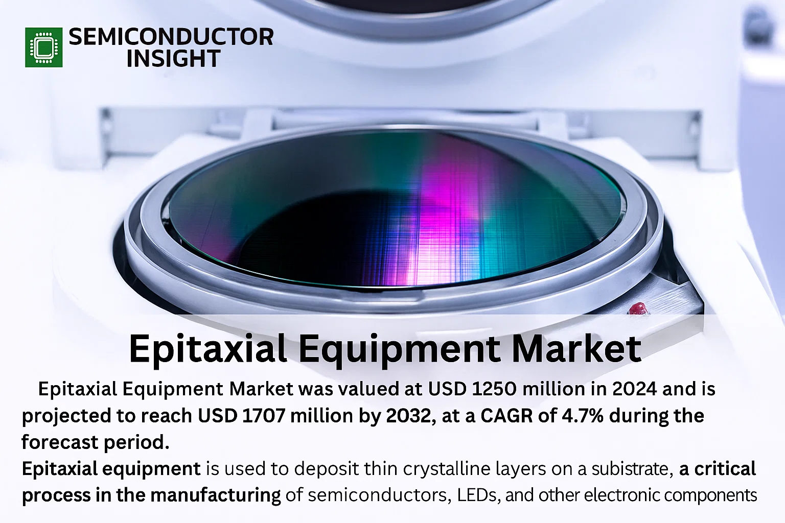
Global Epitaxial Equipment Market was valued at USD 1250 million in 2024 and is projected to reach USD 1707 million by 2032, at a CAGR of 4.7% during the forecast period.
Epitaxial equipment is used to deposit thin crystalline layers on a substrate, a critical process in the manufacturing of semiconductors, LEDs, and other electronic components. The market’s growth is primarily driven by the increasing demand for advanced electronics, the proliferation of IoT devices, and the continued expansion of 5G infrastructure. Additionally, the push for more efficient and powerful semiconductor devices in applications like artificial intelligence, autonomous vehicles, and renewable energy systems is fueling demand.
However, the market also faces challenges, including the high cost of advanced epitaxial equipment and the complexity of the deposition processes, which require significant expertise. Geopolitical tensions affecting the semiconductor supply chain also present potential headwinds.
Key players in the market include AIXTRON, Advanced Micro-Fabrication Equipment Inc., Veeco, LPE (Italy), TAIYO NIPPON SANSO, ASMI, Applied Materials, NuFlare, Tokyo Electron, CETC, NAURA, Riber, DCA, Scienta Omicron, Pascal, and Dr. Eberl MBE-Komponenten GmbH, among others.
MARKET DRIVERS
Rising Demand for GaN and SiC Power Electronics
The global push for energy efficiency is fueling the adoption of wide-bandgap semiconductors like Gallium Nitride (GaN) and Silicon Carbide (SiC) in applications ranging from electric vehicles to renewable energy systems. Epitaxial equipment is critical for depositing the high-quality crystalline layers required for these advanced semiconductor devices. The market is experiencing significant growth as production of GaN power ICs and SiC power modules scales up to meet demand.
Proliferation of 5G Infrastructure and RF Devices
The global rollout of 5G networks necessitates advanced radio frequency (RF) components built on compound semiconductors. Epitaxial reactors are essential for producing the Gallium Arsenide (GaAs) and GaN epitaxial wafers used in 5G base station power amplifiers and smartphone front-end modules. This infrastructure build-out represents a major, sustained driver for Metalorganic Chemical Vapor Deposition (MOCVD) and Molecular Beam Epitaxy (MBE) equipment markets.
➤ The compound semiconductor market, heavily reliant on epitaxy, is projected to grow at a CAGR of nearly 9% over the next five years, directly translating to increased equipment sales.
Furthermore, the continuous miniaturization and performance enhancement of optoelectronic devices, including micro-LEDs for displays and VCSELs for 3D sensing, requires increasingly precise and uniform epitaxial growth processes. This technological evolution pushes the demand for next-generation epitaxial tools with enhanced control over layer thickness and material purity.
MARKET CHALLENGES
High Capital Investment and Operational Costs
Epitaxial equipment, particularly advanced MOCVD and MBE systems, represents a significant capital expenditure for semiconductor manufacturers, often costing several million dollars per tool. Furthermore, the operational costs are substantial, involving high-purity precursor gases, specialized substrates, and significant consumption of utilities like power and ultra-pure water. This high cost of ownership can be a barrier to entry for smaller players and requires a clear ROI justification for fab investments.
Other Challenges
Process Complexity and Yield Management
Achieving high yields with complex multi-layer epitaxial structures is technically challenging. Defects, contamination, or non-uniformity during growth can render entire wafers unusable, impacting overall manufacturing profitability. This necessitates highly skilled operators and robust process control, adding to the operational complexity and cost.
Stringent Technical Requirements for Advanced Nodes
As device architectures shrink and new materials are introduced, the specifications for epitaxial layers become increasingly stringent. Equipment manufacturers face the challenge of developing systems that can consistently deliver atomic-level precision, ultra-low defect densities, and high throughput simultaneously, often requiring significant R&D investment.
MARKET RESTRAINTS
Cyclical Nature of the Semiconductor Industry
The epitaxial equipment market is inherently tied to the capital expenditure cycles of the broader semiconductor industry. During periods of downturn or overcapacity, chip manufacturers delay or cancel new equipment purchases, leading to significant volatility in the order book for equipment suppliers. This cyclicality makes long-term planning and revenue stability a major challenge for companies in this space.
Geopolitical Tensions and Trade Policies
Export controls and trade restrictions on advanced semiconductor technology, particularly between major economic blocs, can disrupt the global supply chain for epitaxial equipment. Restrictions on the sale of tools to certain regions or companies can limit market access for equipment vendors and create uncertainty, acting as a restraint on market growth.
Additionally, the long lead times for tool development and qualification mean that equipment suppliers cannot quickly respond to abrupt shifts in market demand. The time from R&D to a fully qualified production-ready tool can span several years, creating a lag between emerging market needs and the availability of suitable equipment.
MARKET OPPORTUNITIES
Expansion in Automotive Semiconductor Applications
The automotive industry’s transformation towards electrification and autonomy is creating massive demand for semiconductors. This includes a surge in requirements for SiC and GaN power devices for electric powertrains and onboard chargers, as well as advanced sensors. This represents a substantial and growing addressable market for epitaxial equipment providers focused on power and optoelectronic applications.
Emergence of New Applications: Quantum Computing and Photonics
Beyond traditional electronics, epitaxial growth is fundamental to emerging fields like quantum computing, where precise material structures are needed for qubits, and integrated photonics, which uses light for data transmission. These nascent but high-growth fields present long-term opportunities for specialized epitaxial equipment capable of meeting unique material and structural requirements.
The push for more sustainable manufacturing processes also opens avenues for innovation. Opportunities exist for equipment that reduces the consumption of hazardous precursors, lowers energy usage, or enables the recycling of process gases. Developing greener epitaxial solutions could become a key differentiator and open up new market segments focused on environmental sustainability.
Epitaxial Equipment Market Trends
Sustained Growth Driven by Electronics Demand
The global Epitaxial Equipment market demonstrates a positive trajectory, valued at approximately $1250 million in 2024 and projected to reach $1707 million by 2032, representing a compound annual growth rate (CAGR) of 4.7%. This expansion is primarily fueled by the ongoing demand for advanced electronic components, particularly in the consumer electronics and optoelectronics sectors. Growth is underpinned by increasing adoption of high-performance semiconductors, which require sophisticated epitaxial deposition processes for manufacturing.
Other Trends
Market Concentration and Regional Leadership
The market is characterized by a high degree of consolidation, with the top four companies collectively holding a dominant share exceeding 56%. Key global players include AIXTRON, Veeco, and Applied Materials. Regionally, North America is the largest market with a share of approximately 25%, followed closely by China at 24% and Japan at 12%. This distribution highlights the critical role of established semiconductor manufacturing hubs and the rapid expansion of the semiconductor industry in Asia.
Segmentation and Technological Advancement
Major equipment types include MOCVD (Metal-Organic Chemical Vapor Deposition) and Molecular Beam Epitaxy (MBE) systems, which are essential for producing high-quality thin films for LEDs, power electronics, and advanced logic chips. The LED industry remains a primary application area for epitaxial equipment. A significant trend is the development of more efficient and precise equipment capable of handling larger wafers and novel materials like gallium nitride (GaN) and silicon carbide (SiC), driven by the need for greater performance and energy efficiency in end-products. The competitive landscape is marked by continuous innovation from leading manufacturers to capture market share in this growing segment.
COMPETITIVE LANDSCAPE
Key Industry Players
Market Concentrated with Four Players Holding Majority Share
The global epitaxial equipment market exhibits a concentrated structure dominated by a handful of technologically advanced players. German-based AIXTRON SE stands as a clear leader in the Metal-Organic Chemical Vapor Deposition (MOCVD) segment, which is critical for manufacturing LEDs and power electronics. Alongside AIXTRON, the top four companies collectively command over 56% of the global market share. These leading firms, including ASM International (ASMI), Veeco Instruments, and NuFlare Technology, possess significant R&D capabilities and extensive patent portfolios, creating high barriers to entry. Their dominance is reinforced by long-standing relationships with major semiconductor manufacturers across key regions like North America, which holds about 25% of the market. The competitive dynamics are shaped by continuous innovation in deposition technologies to achieve higher throughput, lower defect densities, and compatibility with larger wafer sizes.
Beyond the top tier, the market includes several significant players that cater to niche applications or specific geographic markets. Companies such as LPE (Italy) and Riber specialize in Molecular Beam Epitaxy (MBE) systems used for high-precision research and compound semiconductor applications. In Asia, particularly in China and Japan, domestic suppliers like Advanced Micro-Fabrication Equipment Inc. (AMEC), NAURA Technology Group, and Tokyo Electron have gained substantial market presence, supported by regional government initiatives and growing local demand. Other notable participants include Applied Materials, a giant in semiconductor equipment that offers epitaxial solutions, and specialized firms like CETC, DCA Instruments, Scienta Omicron, Pascal, and Dr. Eberl MBE-Komponenten GmbH, which serve specialized research and development sectors. These companies compete on factors such as technology specialization, cost-effectiveness, and local customer support.
List of Key Epitaxial Equipment Companies Profiled
- AIXTRON
- ASM International (ASMI)
- Veeco Instruments
- NuFlare Technology
- Advanced Micro-Fabrication Equipment Inc. (AMEC)
- Applied Materials
- Tokyo Electron
- LPE (Italy)
- TAIYO NIPPON SANSO
- CETC
- NAURA Technology Group
- Riber
- DCA Instruments
- Scienta Omicron
- Pascal
- Dr. Eberl MBE-Komponenten GmbH
Segment Analysis:
| Segment Category | Sub-Segments | Key Insights |
| By Type |
|
MOCVD Equipment stands as the dominant technology pillar within the epitaxial equipment market, primarily driven by its critical role in mass-producing high-performance semiconductors and advanced light-emitting diodes. This segment’s leadership is anchored in its superior capability to deposit high-quality crystalline layers across large-area wafers with exceptional uniformity, which is essential for manufacturing consistency in high-volume fabrication facilities. The continuous innovation aimed at improving throughput and material quality for next-generation power electronics and micro-LED displays further solidifies its prominent position. In contrast, Molecular Beam Epitaxy equipment is revered for its unparalleled precision in creating ultra-pure, atomically sharp interfaces, making it indispensable for cutting-edge research and development activities and specialized low-volume production of high-frequency electronic and photonic devices. |
| By Application |
|
LED Industry is the most significant application segment for epitaxial equipment, serving as the fundamental backbone for the production of LED chips used in everything from general lighting and automotive headlights to full-color displays. The relentless global demand for energy-efficient lighting solutions and the rapid expansion of high-brightness display technologies create a sustained and robust demand for high-throughput MOCVD systems. The Consumer Electronics segment follows closely, leveraging epitaxial processes to manufacture advanced compound semiconductor components that are vital for the functionality of smartphones, high-speed data networks, and power management systems. The “Others” category encompasses promising growth areas such as photovoltaics and specialized sensors, which are gradually adopting epitaxial techniques to enhance device performance and efficiency. |
| By End User |
|
Integrated Device Manufacturers represent the leading end-user segment, as these large-scale semiconductor companies possess the capital and vertical integration necessary to operate sophisticated in-house epitaxial fabrication lines. Their demand is characterized by a need for high-volume, reliable production equipment to maintain supply chains for their diverse electronic products. Foundries constitute another major customer base, providing epitaxial wafer services to fabless semiconductor companies and driving demand for equipment that offers scalability and process versatility. Research and Academic Institutes, while a smaller segment in terms of unit volume, are critically important as innovation hubs. They primarily utilize highly precise, though lower-throughput, equipment like MBE systems to pioneer new materials and device architectures that eventually transition to commercial production. |
| By Wafer Size |
|
200mm wafer capacity represents a highly significant segment, particularly for the manufacturing of a wide array of compound semiconductor devices including many types of LEDs and RF components. This segment benefits from a well-established ecosystem and a balance between production efficiency and technological maturity. The transition towards larger 300mm and Above wafers is a key industry trend driven by the pursuit of greater economies of scale for high-volume silicon-based power devices and advanced photonics, though it presents substantial technical challenges in maintaining epitaxial layer uniformity. The segment for 150mm and Below wafers remains crucial for research, development, and the production of specialized, lower-volume devices where extreme material quality is paramount over sheer production volume. |
| By Material |
|
Gallium-Based materials, particularly Gallium Nitride (GaN) and Gallium Arsenide (GaAs), form the leading material segment due to their exceptional electronic and optoelectronic properties which are fundamental to modern power electronics, RF amplifiers, and LED technologies. The intense focus on developing wide-bandgap semiconductors for efficient energy conversion and high-frequency applications underpins the strong demand for equipment capable of processing these materials. The Silicon segment remains a massive and foundational market, especially for epitaxial layers used in advanced CMOS applications and silicon-based power devices. The segment for Other Compound Semiconductors includes promising materials like silicon carbide and indium phosphide, which are gaining traction for specialized high-power and photonic applications, representing a frontier for equipment innovation. |
Regional Analysis: Epitaxial Equipment Market
Taiwan and South Korea are the core drivers of the regional market, home to the world’s leading pure-play semiconductor foundries. These companies are in a perpetual race for process node miniaturization, requiring extremely precise epitaxial equipment to create the sophisticated transistor structures essential for advanced logic and memory chips. The continuous capex cycles of these giants ensure a consistent and technologically demanding market for epitaxial tool suppliers, focusing on purity, uniformity, and process control to meet the stringent requirements of sub-5nm technology nodes.
China’s market dynamics are defined by a concerted national strategy to achieve semiconductor self-sufficiency. This has led to the rapid construction of new fabs, creating a surge in demand for all semiconductor manufacturing equipment, including epitaxial systems. While initially focused on mature nodes, the push is increasingly towards more advanced applications, particularly for power electronics using SiC and GaN epitaxy to support the country’s dominant electric vehicle and renewable energy sectors, representing a significant growth vector.
Japan’s strength lies in its world-leading expertise in high-purity semiconductor materials and its position as a key supplier of critical components used within epitaxial reactors themselves. Japanese firms are leaders in compound semiconductor epitaxy, especially for optoelectronics like lasers and LEDs. The market is characterized by a focus on high-value, specialized epitaxial equipment and consumables, catering to niche applications with demanding material quality specifications.
The broader Asia-Pacific region, including Southeast Asia and Australasia, plays a crucial supporting role. Countries like Singapore and Malaysia host important back-end manufacturing and packaging facilities, while Australia possesses strong research capabilities in compound semiconductors. The market dynamics here involve demand for epitaxial equipment related to specialized research, pilot production lines, and supporting the region’s growing electronics manufacturing base, adding diversity to the overall regional demand.
North America
North America maintains a strong position in the epitaxial equipment market, characterized by high-value, innovation-driven demand. The region is a global hub for fabless semiconductor companies and integrated device manufacturers (IDMs) that focus on cutting-edge design and specialized manufacturing. Demand is particularly strong for epitaxial systems used in the development and initial production of next-generation chips for artificial intelligence, high-performance computing, and advanced defense applications. There is a significant emphasis on compound semiconductor epitaxy, with substantial investments in GaN and SiC technologies for power electronics and RF devices. The presence of leading equipment manufacturers and a robust R&D ecosystem, including major universities and national laboratories, fuels a market that prioritizes technological leadership and customization over pure volume, driving the need for highly advanced and flexible epitaxial tools.
Europe
The European epitaxial equipment market is distinguished by its focus on industrial and automotive applications, underpinned by strong collaborative research initiatives. The region’s automotive industry, a global leader in premium and electric vehicles, is a primary driver, creating sustained demand for epitaxial equipment capable of producing high-reliability SiC and GaN power semiconductors. Major collaborative programs, such as those funded by the European Union, foster innovation in semiconductor materials and processes, stimulating demand for advanced R&D-grade epitaxial systems. The market is also supported by a network of specialized IDMs and research institutes with deep expertise in areas like micro-electromechanical systems (MEMS) and photonics, leading to a need for precise, application-specific epitaxial solutions rather than high-volume production tools.
South America
The epitaxial equipment market in South America is nascent but shows potential for gradual growth, primarily driven by regional industrial development and academic research. The market dynamics are currently defined by limited local semiconductor manufacturing, with demand concentrated in university laboratories and a few industrial research centers focusing on materials science. There is sporadic interest in epitaxial equipment for developing semiconductor applications relevant to local industries, such as sensors for agriculture and mining or optoelectronics. While not a major volume market, it represents an emerging opportunity for suppliers of benchtop or smaller-scale epitaxial systems aimed at research and prototype development, with growth tied to broader regional technological and economic advancement.
Middle East & Africa
The epitaxial equipment market in the Middle East and Africa is the smallest globally, characterized by very limited indigenous semiconductor fabrication. Market activity is almost exclusively confined to academic and research institutions in a few countries, such as Israel, Saudi Arabia, and South Africa, which invest in epitaxial tools for fundamental research in nanotechnology and new materials. Some nations in the Gulf region are initiating long-term technology diversification plans, which could eventually include investments in semiconductor-related infrastructure. However, current dynamics involve minimal commercial demand, with the market primarily consisting of niche opportunities for research-grade equipment supporting scientific advancement rather than industrial production.
Report Scope
This market research report provides a comprehensive analysis of the Epitaxial Equipment Market , covering the forecast period 2025–2032. It offers detailed insights into market dynamics, technological advancements, competitive landscape, and key trends shaping the industry.
Key focus areas of the report include:
- Market Overview: The report begins with an overview outlining its current market scenario, key growth indicators, and industry transformation drivers. It discusses macroeconomic factors, demand–supply balance, regulatory landscape, and the strategic role of semiconductors in powering advancements across industries such as automotive, telecommunications, consumer electronics, and industrial automation.
- Market Size & Forecast: Historical data and future projections for revenue, unit shipments, and market value across major regions and segments.
- Segmentation Analysis: Detailed breakdown by product type, technology, application, and end-user industry to identify high-growth segments and investment opportunities.
- Regional Insights: Insights into market performance across North America, Europe, Asia-Pacific, Latin America, and the Middle East & Africa, including country-level analysis where relevant.
- Competitive Landscape: Profiles of leading market participants, including their product offerings, R&D focus, manufacturing capacity, pricing strategies, and recent developments such as mergers, acquisitions, and partnerships.
- Technology Trends & Innovation: Assessment of emerging technologies, integration of AI/IoT, semiconductor design trends, fabrication techniques, and evolving industry standards.
- Market Drivers & Restraints: Evaluation of factors driving market growth along with challenges, supply chain constraints, regulatory issues, and market-entry barriers.
- Stakeholder Insights: Insights for component suppliers, OEMs, system integrators, investors, and policymakers regarding the evolving ecosystem and strategic opportunities.
Primary and secondary research methods are employed, including interviews with industry experts, data from verified sources, and real-time market intelligence to ensure the accuracy and reliability of the insights presented.
FREQUENTLY ASKED QUESTIONS:
What is the current market size of Epitaxial Equipment Market?
-> Global Epitaxial Equipment Market was valued at USD 1250 million in 2024 and is projected to reach USD 1707 million by 2032, exhibiting a CAGR of 4.7% during the forecast period.
Which key companies operate in Epitaxial Equipment Market?
-> Key players include AIXTRON, Advanced Micro-Fabrication Equipment Inc, ASMI, NuFlare, Veeco, and TAIYO NIPPON SANSO, among others. The global top four companies hold a share over 56%.
What are the key growth drivers?
-> Key growth drivers include advancements in the semiconductor industry, rising demand from the LED and consumer electronics sectors, and increased investment in R&D for next-generation devices.
Which region dominates the market?
-> North America is the largest market with a share of about 25%, followed by China and Japan with shares of about 24% and 12%, respectively.
What are the emerging trends?
-> Emerging trends include the development of advanced CVD and MBE equipment, increasing adoption in power electronics and photonics applications, and technological innovations aimed at improving deposition precision and efficiency.

Get Sample Report PDF for Exclusive Insights
Report Sample Includes
- Table of Contents
- List of Tables & Figures
- Charts, Research Methodology, and more...
 Download Sample Report PDF