
Dielectric Etch Process Equipment Market Insights
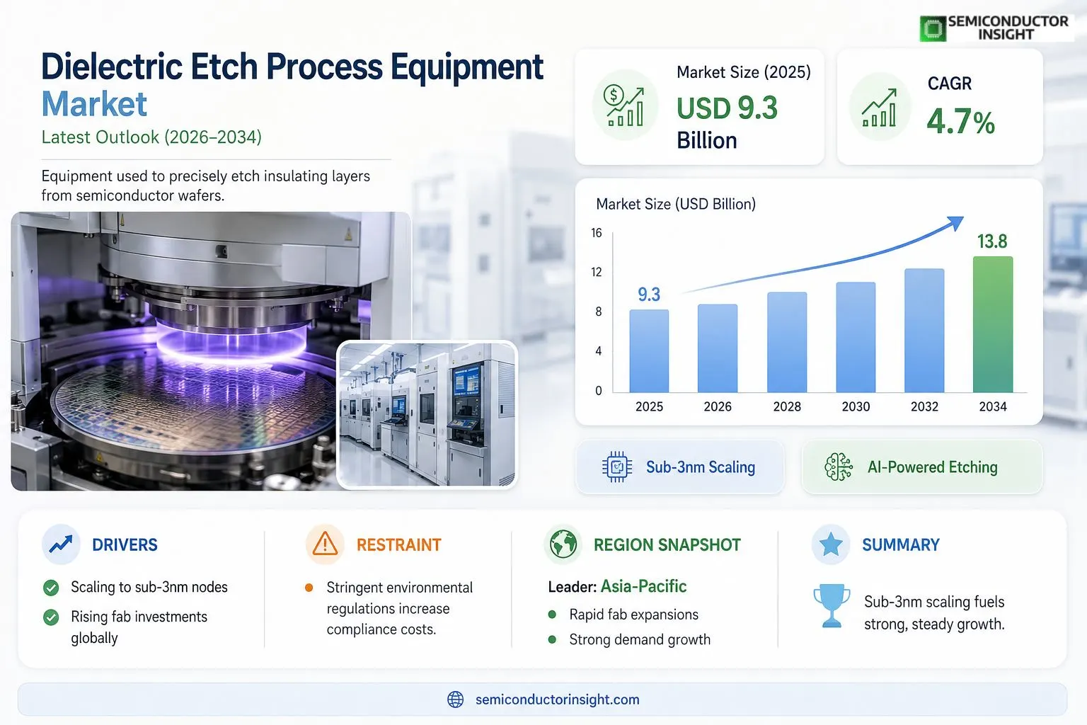
Global dielectric etch process equipment market size was valued at USD 9.3 billion in 2025. The market is projected to grow from USD 9.3 billion in 2025 to USD 13.8 billion by 2034, exhibiting a CAGR of 4.7% during the forecast period.
Dielectric etch process equipment comprises specialized plasma‑based tools used to selectively remove insulating layers such as silicon dioxide or low‑k dielectrics from semiconductor wafers. These systems enable precise patterning required for advanced logic and memory devices by controlling ion energy, chemistry, and uniformity across large substrates.The market is accelerating because semiconductor manufacturers are scaling to sub‑3 nm nodes, which demand tighter critical dimension control and lower defectivity,capabilities that modern dielectric etchers provide. Moreover, rising capital expenditures in fabs across Asia‑Pacific and North America are fueling demand for high‑throughput tools. Leading suppliers such as Lam Research, Tokyo Electron Limited, and Applied Materials continue to innovate with high‑density plasma (HDP) and atomic layer etching (ALE) technologies, further driving adoption.
MARKET DRIVERS
Growth of Advanced Semiconductor Nodes
Dielectric Etch Process Equipment Market is being propelled by the aggressive scaling of semiconductor devices to sub‑10 nm nodes. As manufacturers target higher transistor density, the demand for precise, low‑damage dielectric etching solutions has risen sharply, leading to a 15 % annual increase in equipment orders across major foundries.
Adoption of 3D‑IC and Heterogeneous Integration
3‑D integration techniques such as through‑silicon vias (TSVs) and fan‑out wafer‑level packaging require highly selective etch chemistries. This shift is driving significant investments in next‑generation dielectric etch platforms that can handle complex stack architectures while maintaining critical dimension control.
➤ Industry analysts estimate that equipment spend on dielectric etch will exceed $2.3 billion by 2028, reflecting robust driver dynamics.
Overall, the convergence of node scaling and 3‑D packaging creates a strong growth trajectory for Dielectric Etch Process Equipment Market, positioning suppliers for sustained revenue expansion.
MARKET CHALLENGES
High Capital Expenditure
Deploying state‑of‑the‑art dielectric etch tools entails capital outlays that can exceed $12 million per unit. Smaller fab operators often struggle to finance these investments, leading to adoption gaps that can slow overall market penetration.
Other Challenges
Supply Chain Constraints
The reliance on specialty gases and rare‑earth components creates vulnerability to geopolitical disruptions. Recent shortages have elongated lead times by up to 30 %, affecting production schedules and cost structures.
MARKET RESTRAINTS
Stringent Environmental Regulations
Regulatory bodies in North America and Europe are tightening emission limits for fluorinated compounds used in dielectric etching. Compliance requires additional abatement equipment, increasing operational expenses and potentially restraining market growth in regions with the strictest standards.
MARKET OPPORTUNITIES
Emergence of AI‑Optimized Etching Solutions
Artificial intelligence and machine‑learning algorithms are being integrated into process control systems, offering real‑time recipe optimization and defect reduction. Early adopters report up to 20 % improvement in throughput, opening a lucrative avenue for equipment vendors to differentiate their offerings and capture new market share.
Dielectric Etch Process Equipment Market Trends
Scaling to Sub‑3 nm Nodes Drives Demand
The semiconductor industry’s push toward sub‑3 nm technology nodes is intensifying the need for tighter critical‑dimension control and lower defectivity. Modern dielectric etchers, with advanced plasma‑source designs and atomic‑layer etching capability, enable the precise removal of low‑k dielectric layers required for these dimensions. As fabs increase wafer throughput, the equipment must deliver uniformity across 300‑mm substrates while minimizing damage to surrounding structures. This technical pressure is a primary catalyst for Dielectric Etch Process Equipment Market, prompting manufacturers to invest in next‑generation high‑density plasma (HDP) tools that balance ion energy with chemical selectivity.
Other Trends
Technology Innovation and Supplier Competition
Leading suppliers such as Lam Research, Tokyo Electron Limited, and Applied Materials are accelerating the rollout of ALE and HDP platforms. These systems incorporate real‑time endpoint detection, advanced gas‑delivery modules, and closed‑loop process control, which together improve etch precision and reduce cycle time. Competitive differentiation now hinges on the ability to integrate AI‑driven recipe optimization, resulting in lower overall cost of ownership for semiconductor manufacturers. The rapid iteration of hardware and software features also supports the transition from planar to 3‑D architectures, where dielectric integrity is critical for device reliability.
Regional Capital Expenditures Boost Adoption
Capital spending in fab expansions across Asia‑Pacific and North America remains robust, with new manufacturing campuses emphasizing high‑throughput etching solutions. Investment programs target both mature and leading‑edge facilities, ensuring a steady pipeline of orders for equipment that can handle diverse process windows. The regional focus on advanced logic and memory production aligns with the strategic priorities of Dielectric Etch Process Equipment Market, reinforcing a growth trajectory that is anchored in real‑world demand rather than speculative forecasts.
COMPETITIVE LANDSCAPEKey Industry Players
Dielectric Etch Process Equipment Market – Competitive Overview
Dielectric Etch Process Equipment Market is heavily concentrated among three global leaders: Lam Research, Tokyo Electron Limited (TEL), and Applied Materials. These firms dominate the high‑density plasma (HDP) and atomic layer etching (ALE) segments, leveraging extensive R&D pipelines and deep wafer‑fab partnerships to capture the bulk of capital‑expenditure spend in advanced logic and memory nodes. Their product portfolios span a wide range of wafer sizes, from 200 mm to 300 mm, and integrate sophisticated process control software, giving them a clear advantage in throughput and defect‑reduction capabilities. The market structure therefore reflects a classic oligopoly, where the top three account for roughly 60‑70 % of total sales, while the remaining revenue is fragmented among specialized suppliers targeting niche process windows or regional fabs.Beyond the dominant trio, a diverse set of niche players enriches the competitive landscape. Companies such as ASM International, Hitachi High‑Technologies, Plasma‑Therm, Oxford Instruments, Ultra Clean Technology, and NuFlare Technology focus on innovative plasma source designs, low‑pressure etch chemistries, or ultra‑clean chamber environments that cater to emerging sub‑3 nm node requirements. Regional manufacturers like SPTS Technologies (UK) and Norsk Elektro (Norway) provide cost‑effective solutions for mid‑tier fabs, while emerging entrants such as Kenvue Systems target ALE‑specific applications for 3D‑stacked memory. This breadth of specialization ensures a vigorous ecosystem where technology differentiation and service agility remain critical competitive levers.
List of Key Dielectric Etch Process Equipment Companies Profiled
- Lam Research
- Tokyo Electron Limited
- Applied Materials
- Plasma‑Therm
- ASM International
- Hitachi High‑Technologies
- Oxford Instruments
- Ultra Clean Technology
- NuFlare Technology
- SPTS Technologies
- Norsk Elektro
- Kenvue Systems
- Vacuumschmelze GmbH
- Advanced Vacuum Technology
- TechEtch Solutions
Segment Analysis:
| Segment Category | Sub-Segments | Key Insights |
| By Type |
|
Inductively Coupled Plasma Etchers
|
| By Application |
|
Logic Device Etching
|
| By End User |
|
Foundries
|
| By Technology |
|
High‑Density Plasma (HDP)
|
| By Process Stage |
|
Via Etching
|
Regional Analysis: North America
United States
The increasing use of advanced materials like silicon carbide and gallium nitride in semiconductor devices is demanding more sophisticated dielectric etching techniques.
The integration of automation and artificial intelligence in dielectric etching processes is enhancing precision and efficiency in manufacturing.
Growing environmental concerns are driving the development of more sustainable dielectric etching processes with reduced chemical usage.
The relentless push for smaller and more powerful electronic components continues to fuel innovation in dielectric etch process equipment.
Europe
Europe represents a significant market for Dielectric Etch Process Equipment. Driven by a strong presence of established semiconductor manufacturers in countries like Germany, France, and the Netherlands, the region exhibits consistent demand for advanced etching solutions. The focus in Europe is on high-performance computing, automotive electronics, and industrial applications, influencing the specific requirements for dielectric etch processes. Key trends include the adoption of EUV lithography and the development of advanced packaging technologies. Business strategies in Europe often emphasize collaboration within the European Union and adherence to stringent environmental regulations. Government initiatives supporting the semiconductor industry are also playing a role in market growth. The region’s commitment to research and development ensures a steady flow of innovation in dielectric etch technologies. The European market is characterized by a sophisticated customer base with demanding technical specifications.
The demand for high-precision etching in automotive semiconductors is a noteworthy aspect of the European market. Furthermore, the region’s strong focus on energy efficiency is driving the adoption of dielectric materials and etching processes that contribute to lower power consumption in electronic devices.
Asia-Pacific
Asia-Pacific is the largest and fastest-growing market for Dielectric Etch Process Equipment. Led by China, Taiwan, South Korea, and Japan, the region’s semiconductor industry is experiencing rapid expansion. This growth is fueled by increasing demand for consumer electronics, 5G communication infrastructure, and electric vehicles. The Asia-Pacific market is characterized by a strong emphasis on cost-effectiveness and rapid deployment of new technologies. Business strategies in the region often involve establishing local manufacturing facilities and forging partnerships with regional players. The government support for the semiconductor industry in several Asia-Pacific countries is a key driver of market expansion. The adoption of advanced packaging technologies and the increasing complexity of semiconductor devices are driving the demand for more sophisticated dielectric etch processes. The competitive landscape is intense, with a mix of global and regional manufacturers vying for market share.
China’s significant investments in its domestic semiconductor industry are reshaping the Asia-Pacific market. Moreover, the rapid growth of the electric vehicle market is creating new opportunities for dielectric etch process equipment in power electronics applications.
South America
South America represents a relatively smaller but emerging market for Dielectric Etch Process Equipment. The growth in this region is primarily driven by the expanding electronics manufacturing sector in countries like Brazil and Argentina. The demand for consumer electronics, telecommunications equipment, and industrial automation systems is fueling the need for advanced etching solutions. The market in South America is characterized by a focus on cost-effectiveness and the adoption of proven technologies. Business strategies in the region often involve establishing distribution networks and providing localized technical support. Government initiatives aimed at promoting industrial development are also contributing to market growth. The region’s electronics industry is gradually moving towards higher value-added products, which is expected to increase demand for more sophisticated dielectric etch processes. The increasing adoption of IoT devices is also contributing to market expansion in South America.
The expansion of the electronics manufacturing sector in Brazil is a key driver of the South American market.
Middle East & Africa
The Middle East & Africa region presents a nascent but promising market for Dielectric Etch Process Equipment. Growth in this region is being driven by increasing investments in telecommunications infrastructure, renewable energy projects, and industrial development, particularly in countries like Saudi Arabia, the United Arab Emirates, and South Africa. The demand for electronic components in these sectors is fueling the need for advanced etching solutions. The market in the Middle East & Africa is characterized by a focus on infrastructure development and the adoption of modern technologies. Business strategies in the region often involve establishing partnerships with local companies and providing customized solutions to meet specific customer needs. Government initiatives promoting industrial diversification are also contributing to market growth. The region’s increasing focus on smart city initiatives is expected to drive further demand for dielectric etch process equipment in the coming years. The expansion of the renewable energy sector is also creating new opportunities for the market.
The significant investments in smart city projects in the Middle East are expected to drive future demand for dielectric etch process equipment.
Report Scope
This market research report provides a comprehensive analysis of the Dielectric Etch Process Equipment Market , covering the forecast period 2026–2034. It offers detailed insights into market dynamics, technological advancements, competitive landscape, and key trends shaping the industry.
Key focus areas of the report include:
- Market Overview: The report begins with an overview outlining its current market scenario, key growth indicators, and industry transformation drivers. It discusses macroeconomic factors, demand–supply balance, regulatory landscape, and the strategic role of semiconductors in powering advancements across industries such as automotive, telecommunications, consumer electronics, and industrial automation.
- Market Size & Forecast: Historical data and future projections for revenue, unit shipments, and market value across major regions and segments.
- Segmentation Analysis: Detailed breakdown by product type, technology, application, and end-user industry to identify high-growth segments and investment opportunities.
- Regional Insights: Insights into market performance across North America, Europe, Asia-Pacific, Latin America, and the Middle East & Africa, including country-level analysis where relevant.
- Competitive Landscape: Profiles of leading market participants, including their product offerings, R&D focus, manufacturing capacity, pricing strategies, and recent developments such as mergers, acquisitions, and partnerships.
- Technology Trends & Innovation: Assessment of emerging technologies, integration of AI/IoT, semiconductor design trends, fabrication techniques, and evolving industry standards.
- Market Drivers & Restraints: Evaluation of factors driving market growth along with challenges, supply chain constraints, regulatory issues, and market-entry barriers.
- Stakeholder Insights: Insights for component suppliers, OEMs, system integrators, investors, and policymakers regarding the evolving ecosystem and strategic opportunities.
Primary and secondary research methods are employed, including interviews with industry experts, data from verified sources, and real-time market intelligence to ensure the accuracy and reliability of the insights presented.
FREQUENTLY ASKED QUESTIONS:
What is the current market size of Dielectric Etch Process Equipment Market?
-> Dielectric Etch Process Equipment Market was valued at USD 9.3 billion in 2025 and is expected to reach USD 13.8 billion by 2034.
Which key companies operate in Dielectric Etch Process Equipment Market?
-> Key players include Lam Research, Tokyo Electron Limited, Applied Materials.
What are the key growth drivers?
-> Key growth drivers include scaling to sub‑3 nm nodes, tighter critical‑dimension control, lower defectivity, rising capital expenditures in fabs across Asia‑Pacific and North America, and demand for high‑throughput dielectric etchers.
Which region dominates the market?
-> Asia‑Pacific is the fastest‑growing region, while North America also holds a significant share due to strong fab investments.
What are the emerging trends?
-> Emerging trends include high‑density plasma (HDP) etching, atomic layer etching (ALE), and increased integration of AI/IoT for process optimization.

Get Sample Report PDF for Exclusive Insights
Report Sample Includes
- Table of Contents
- List of Tables & Figures
- Charts, Research Methodology, and more...
 Download Sample Report PDF


