
Die-to-Wafer (D2W) Collective Bonding Market Insights
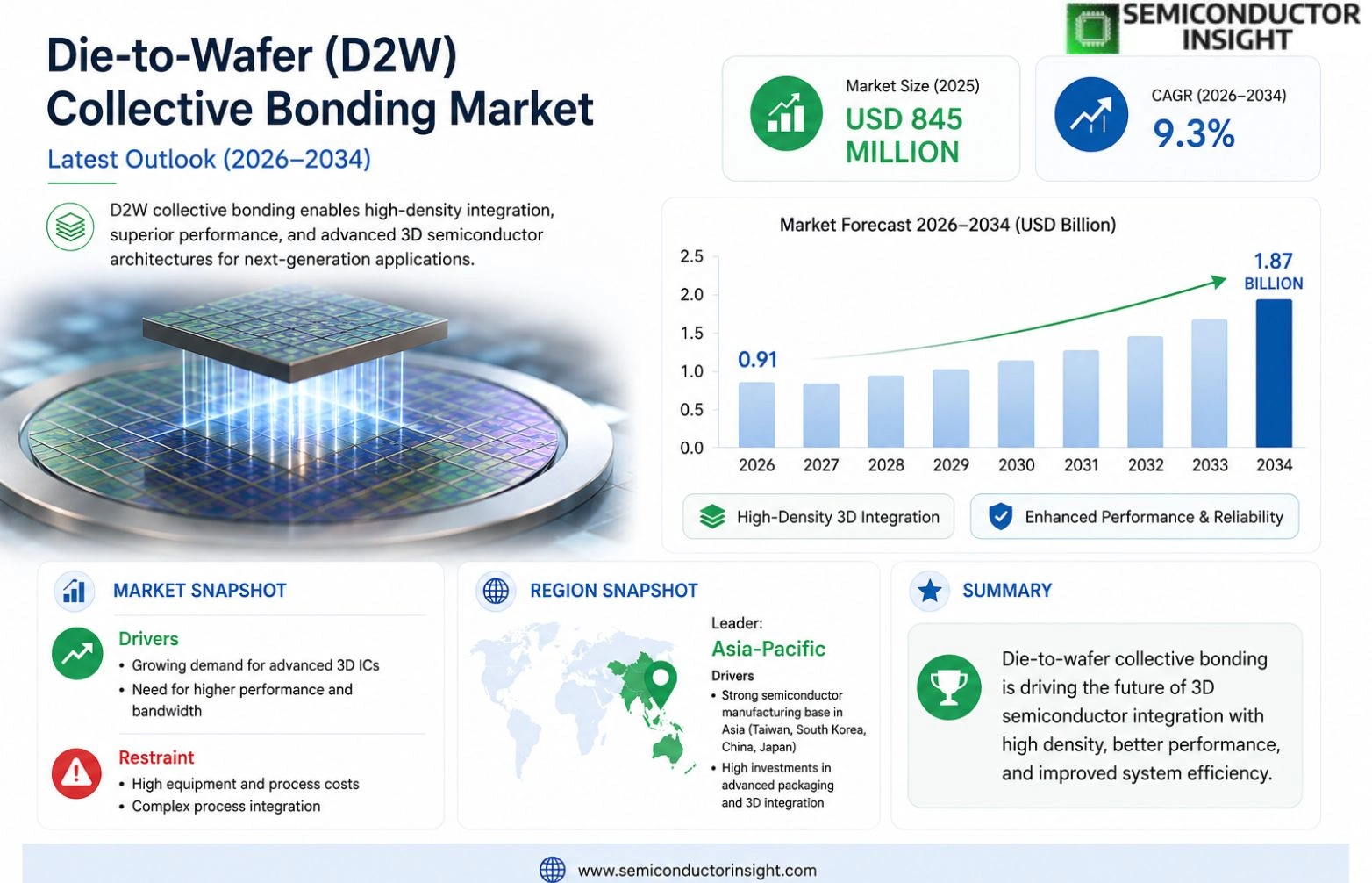
Global Die-to-Wafer (D2W) Collective Bonding market size was valued at USD 845 million in 2025. The market is projected to grow from USD 910 million in 2026 to USD 1.87 billion by 2034, exhibiting a CAGR of 9.3% during the forecast period.
Die-to-Wafer (D2W) Collective Bonding is an advanced semiconductor packaging technique that enables the direct attachment of individual dies onto a wafer substrate, enhancing integration density and electrical performance. This process leverages precision alignment and bonding technologies, including thermocompression bonding, hybrid bonding, and eutectic bonding, to create high-density interconnects essential for applications such as 3D integrated circuits (3D ICs), memory stacks, and heterogeneous integration. By facilitating miniaturization and improved thermal management, D2W collective bonding addresses critical demands in high-performance computing, artificial intelligence (AI), and consumer electronics, positioning it as a pivotal technology in next-generation semiconductor manufacturing.
The market is witnessing robust expansion due to the escalating need for compact, high-efficiency electronic devices coupled with advancements in heterogeneous integration and system-in-package (SiP) solutions. Furthermore, strategic collaborations among industry leaders are accelerating innovation; for instance, in March 2024, Besi and Imec announced a partnership to develop scalable D2W collective bonding processes for mass production. Key players such as ASM Pacific Technology, Besi, EV Group, and TEL are driving technological breakthroughs through substantial R&D investments, reinforcing the market’s upward trajectory.
MARKET DRIVERS
Surge in Demand for 3D Integration
Die-to-Wafer (D2W) Collective Bonding Market is experiencing substantial growth primarily due to the escalating need for three-dimensional semiconductor packaging. As Moore’s Law slows, manufacturers are turning to advanced packaging solutions to increase transistor density without shrinking the die size. Collective bonding offers a robust method to stack multiple dies vertically, thereby enhancing the performance of complex systems-in-package (SiP) without compromising on thermal efficiency.
Enhanced Electrical and Thermal Performance
Efficient power delivery and heat dissipation are critical factors driving the adoption of D2W collective bonding in the global market. This technology reduces parasitic capacitance and inductance compared to wire bonding or flip-chip technologies, which is essential for high-frequency applications. Improved signal integrity and lower thermal resistance make this solution a preferred choice for automotive power modules and industrial IoT devices.
➤ Analyst Insight: The drive for miniaturization without loss of performance is the single largest catalyst for growth in this sector.
Additionally, the reduction in interconnect length improves overall system stability and energy efficiency.
MARKET CHALLENGES
High Complexity in Manufacturing
Navigating Die-to-Wafer (D2W) Collective Bonding Market requires overcoming significant manufacturing complexities. The process demands extremely clean environments and precise control over surface topography. Even minor imperfections on the surfaces of the dies or wafers can result in voids or defects that render the assembly unusable, thereby complicating the mass production timeline.
Other Challenges
Significant Capital Expenditure
Establishing production lines capable of handling collective bonding requires investment in specialized equipment such as plasma cleaning systems and high-precision bonding tools.
Limited Material Compatibility
Not all bonding adhesives and interlayers are suitable for collective bonding, which can restrict the design flexibility for certain semiconductor architectures.
MARKET RESTRAINTS
Compatibility with Advanced Materials
A key restraint Die-to-Wafer (D2W) Collective Bonding Market is the challenge of integrating new advanced materials. As the industry moves towards newer dielectric materials and heterogeneous integration, ensuring that the bonding process does not degrade the properties of these materials remains a technical hurdle. Material incompatibility can lead to increased failure rates in the final product.
MARKET OPPORTUNITIES
Expansion in Heterogeneous Integration
The development of silicon interposers presents a vital opportunity for Die-to-Wafer (D2W) Collective Bonding Market. By enabling the efficient bonding of different types of dies with varying specifications onto a single wafer, this technology allows for the creation of highly sophisticated systems. The rise of AI and high-performance computing is expected to fuel a sharp increase in such interposer applications in the coming years.
Trends
Technological Advancements in Semiconductor Packaging
Die-to-Wafer (D2W) Collective Bonding is an advanced semiconductor packaging technique that enables the direct attachment of individual dies onto a wafer substrate, enhancing integration density and electrical performance. This process leverages precision alignment and bonding technologies, including thermocompression bonding, hybrid bonding, and eutectic bonding, to create high-density interconnects essential for applications such as 3D integrated circuits (3D ICs), memory stacks, and heterogeneous integration. By facilitating miniaturization, D2W collective bonding addresses critical demands in high-performance computing, artificial intelligence (AI), and consumer electronics, effectively positioning itself as a pivotal technology for the next-generation semiconductor manufacturing landscape.
Other Trends
Key Bonding Technologies and Applications
The versatility of D2W bonding allows developers to optimize performance based on specific application requirements. The utilization of hybrid bonding, for instance, supports advanced memory stacks, while thermocompression bonding often caters to standard logic devices. This technological adaptability is vital for maintaining the efficiency of system-in-package (SiP) solutions, which increasingly require the seamless integration of various materials to create superior electronic devices.
Strategic Collaborations and Infrastructure Development
The market is witnessing robust expansion due to the escalating need for compact, high-efficiency electronic devices coupled with advancements in heterogeneous integration and system-in-package (SiP) solutions. Furthermore, strategic collaborations among industry leaders are accelerating innovation; for instance, in March 2024, Besi and Imec announced a partnership to develop scalable D2W collective bonding processes for mass production. Key players such as ASM Pacific Technology, Besi, EV Group, and TEL are driving technological breakthroughs through substantial R&D investments, reinforcing the market’s upward trajectory by ensuring the availability of critical packaging infrastructure.
COMPETITIVE LANDSCAPE
Key Industry Players
Global D2W Collective Bonding Market Analysis and Technology Trends
The competitive landscape for Die-to-Wafer (D2W) Collective Bonding Market is defined by the dominance of established semiconductor equipment manufacturers focused on high-density integration. These key industry players are aggressively investing in research to innovate thermocompression, hybrid, and eutectic bonding technologies essential for 3D integrated circuits. As demand for AI and high-performance computing solutions rises, the market structure is consolidating, with leaders prioritizing reliability and yield improvements in their collective bonding processes to cater to advanced system-in-package applications.
A significant aspect of this landscape involves strategic collaborations between equipment vendors and research institutes to develop scalable production processes. Recent initiatives, such as the pivotal partnership in March 2024 between Besi and Imec, underscore the industry’s move toward standardized D2W solutions for mass fabrication. Additionally, specialized niche players contribute by providing unique materials and laser bonding technologies, ensuring a diverse and resilient ecosystem that addresses complex thermal management and electrical performance requirements.
List of Key D2W Collective Bonding Companies Profiled
- ASM Pacific Technology
- Besi
- EV Group
- Tokyo Electron (TEL)
- Applied Materials
- Kulicke & Soffa
- TSV Technology
- Microconnects
- Coherent
- SUSS MicroTec
- FormFactor
- J-Devices
- Hoya Corporation
- NSG Group
- JPT Corp.
Segment Analysis:
| Segment Category | Sub-Segments | Key Insights |
| By Type |
|
Hybrid Bonding dominates the landscape due to its superior capability for sub-micron interconnects, which is essential for next-generation semiconductor requirements. Thermocompression bonding remains a robust choice for its high reliability in high-temperature environments and well-established process maturity. |
| By Application |
|
High-Performance Computing & AI are primary drivers, necessitating advanced thermal management and signal integrity that D2W technology uniquely provides. The trend towards System-in-package (SiP) architectures is accelerating as the industry seeks to merge logic and memory technologies without sacrificing physical density. |
| By End User |
|
Semiconductor Foundries are the leading segment, heavily investing in packaging infrastructure to maintain technological leadership in advanced manufacturing. OEMs are pivoting towards integrated solutions to reduce system complexity and cost while meeting escalating performance expectations in the consumer market. |
| By Integration Technology |
|
Heterogeneous Integration is critical for combining distinct technologies,such as logic, memory, and sensors,onto a single die, which drastically reduces power consumption and latency. This approach fundamentally redefines system architecture by allowing diverse materials to coexist within a unified package structure. |
| By Process Capability |
|
Scalable Mass Production remains a key focus area as the industry transitions from laboratory prototyping. Successful adoption requires robust yield management and precise alignment technologies to ensure consistency across large wafer volumes, reducing overall manufacturing costs. |
Regional Analysis: Die-to-Wafer (D2W) Collective Bonding Market
North America
The expansion of manufacturing capabilities in the United States and Canada is reshaping the Die-to-Wafer Collective Bonding Market landscape. By leveraging the technical advantages of the Die-to-Wafer Collective Bonding Market, local fabs are reducing thermal stress during wafer processing. The emphasis on next-generation packaging solutions is a key driver, pushing suppliers to optimize production lines for high yield and reliability.
Die-to-Wafer technology is critical for the automotive sector’s transition toward electric and autonomous vehicles. As the Die-to-Wafer Collective Bonding Market adapts, it caters to the rigorous thermal and electrical specifications required by next-gen power modules. The region’s focus on solid-state integration supports higher performance levels with greater durability in critical applications.
Regional players are implementing sophisticated logistics to support the Die-to-Wafer Collective Bonding Market. Collaborative efforts drive efficiency, ensuring that collective bonding materials reach fabrication facilities with minimal delay. Strong industry standards established in North America provide a benchmark for quality and precision, reinforcing the Die-to-Wafer Collective Bonding Market’s stability.
Research institutions are closely aligned with private industry to advance Die-to-Wafer Collective Bonding Market capabilities. This synergy fosters the development of novel bonding chemistries that withstand extreme operating conditions. The drive toward hybrid integration technologies signifies a promising future for the Die-to-Wafer Collective Bonding Market in this region.
Europe
Europe is establishing a strong foothold in the Die-to-Wafer Collective Bonding Market, primarily fueled by the automotive industry’s demand for efficient power management and thermal dissipation. With strict environmental regulations accelerating the shift toward electrified mobility, European manufacturers are integrating advanced collective bonding. The Die-to-Wafer Collective Bonding Market in Europe relies heavily on the synergy between research labs and established automotive giants. The focus remains on creating robust, reliable packaging that supports complex circuitry for intelligent transportation systems. While capital investment in new fabs is slower compared to other regions, the maturity of the existing supply chain ensures a steady demand for high-quality bonding solutions. The Die-to-Wafer Collective Bonding Market continues to benefit from Europe’s commitment to industrial sovereignty and energy efficiency standards.
Asia-Pacific
Asia-Pacific represents the largest production hub for the Die-to-Wafer Collective Bonding Market, characterized by high-volume fabrication and rapid technological iteration. The region’s dominance is bolstered by the dominance of foundries that specialize in scaling 3D chip stacking. As the global demand for miniaturized electronics grows, the Die-to-Wafer Collective Bonding Market sees rapid adoption of volume production techniques. The local manufacturing ecosystem offers cost advantages and supply chain agility, facilitating quick response times to market shifts. The integration of collective bonding across memory and logic chips is defining the strategic direction of the Die-to-Wafer Collective Bonding Market in this powerhouse region. Strong government initiatives often support this trajectory, ensuring Asia-Pacific remains central to global Die-to-Wafer Collective Bonding Market output.
South America
South America is witnessing a nascent but growing interest in the Die-to-Wafer Collective Bonding Market, driven by the modernization of telecommunications and energy infrastructure. While the volume is currently lower than other regions, the strategic importance of efficient semiconductor packaging is becoming increasingly apparent. The Die-to-Wafer Collective Bonding Market in South America is aligning with broader economic development goals to boost local electronics manufacturing capabilities. Importing advanced packaging technologies, these nations aim to transition from assembly to localized production. The focus remains on integrating Die-to-Wafer Collective Bonding Market solutions that support efficient power distribution and data processing for smart grids and urban planning.
Middle East & Africa
Middle East and Africa are emerging markets for the Die-to-Wafer Collective Bonding Market, heavily influenced by vision-led economic diversification plans, such as the NEOM and Vision 2030 initiatives. The demand is less mature but is rapidly evolving as countries invest in smart city technologies and advanced digital infrastructure. The Die-to-Wafer Collective Bonding Market in this region is characterized by a need for durable electronic components that can withstand harsh environmental conditions. Although supply chains are still developing, the potential for growth in the Die-to-Wafer Collective Bonding Market is significant as these nations seek to upgrade their technological base. Strategic alliances with global tech providers are expected to accelerate the adoption of collective bonding technologies in the region.
Report Scope
This market research report provides a comprehensive analysis of Die-to-Wafer (D2W) Collective Bonding Market, covering the forecast period 2026–2034. It offers detailed insights into market dynamics, technological advancements, competitive landscape, and key trends shaping the industry.
Key focus areas of the report include:
- Market Overview: The report begins with an overview outlining its current market scenario, key growth indicators, and industry transformation drivers. It discusses macroeconomic factors, demand–supply balance, regulatory landscape, and the strategic role of semiconductors in powering advancements across industries such as automotive, telecommunications, consumer electronics, and industrial automation.
- Market Size & Forecast: Historical data and future projections for revenue, unit shipments, and market value across major regions and segments.
- Segmentation Analysis: Detailed breakdown by product type, technology, application, and end-user industry to identify high-growth segments and investment opportunities.
- Regional Insights: Insights into market performance across North America, Europe, Asia-Pacific, Latin America, and the Middle East & Africa, including country-level analysis where relevant.
- Competitive Landscape: Profiles of leading market participants, including their product offerings, R&D focus, manufacturing capacity, pricing strategies, and recent developments such as mergers, acquisitions, and partnerships.
- Technology Trends & Innovation: Assessment of emerging technologies, integration of AI/IoT, semiconductor design trends, fabrication techniques, and evolving industry standards.
- Market Drivers & Restraints: Evaluation of factors driving market growth along with challenges, supply chain constraints, regulatory issues, and market-entry barriers.
- Stakeholder Insights: Insights for component suppliers, OEMs, system integrators, investors, and policymakers regarding the evolving ecosystem and strategic opportunities.
Primary and secondary research methods are employed, including interviews with industry experts, data from verified sources, and real-time market intelligence to ensure the accuracy and reliability of the insights presented.
FREQUENTLY ASKED QUESTIONS:
What is the current market size of Die-to-Wafer (D2W) Collective Bonding Market?
-> Die-to-Wafer (D2W) Collective Bonding market size was valued at USD 845 million in 2025. The market is projected to grow from USD 910 million in 2026 to USD 1.87 billion by 2034, exhibiting a CAGR of 9.3% during the forecast period.
Which key companies operate Die-to-Wafer (D2W) Collective Bonding Market?
-> Key players include ASM Pacific Technology, Besi, EV Group, and TEL, among others.
What are the key growth drivers?
-> Key growth drivers include the escalating need for compact, high-efficiency electronic devices and advancements in heterogeneous integration and system-in-package (SiP) solutions.
Which region dominates the market?
-> Asia-Pacific is a major region with significant market presence due to active semiconductor manufacturing activities.
What are the emerging trends?
-> Emerging trends include 3D integrated circuits (3D ICs), memory stacks, heterogeneous integration, and AI.

Get Sample Report PDF for Exclusive Insights
Report Sample Includes
- Table of Contents
- List of Tables & Figures
- Charts, Research Methodology, and more...
 Download Sample Report PDF


