
Conductor Etch (Metal, Gate) Equipment Market Insights
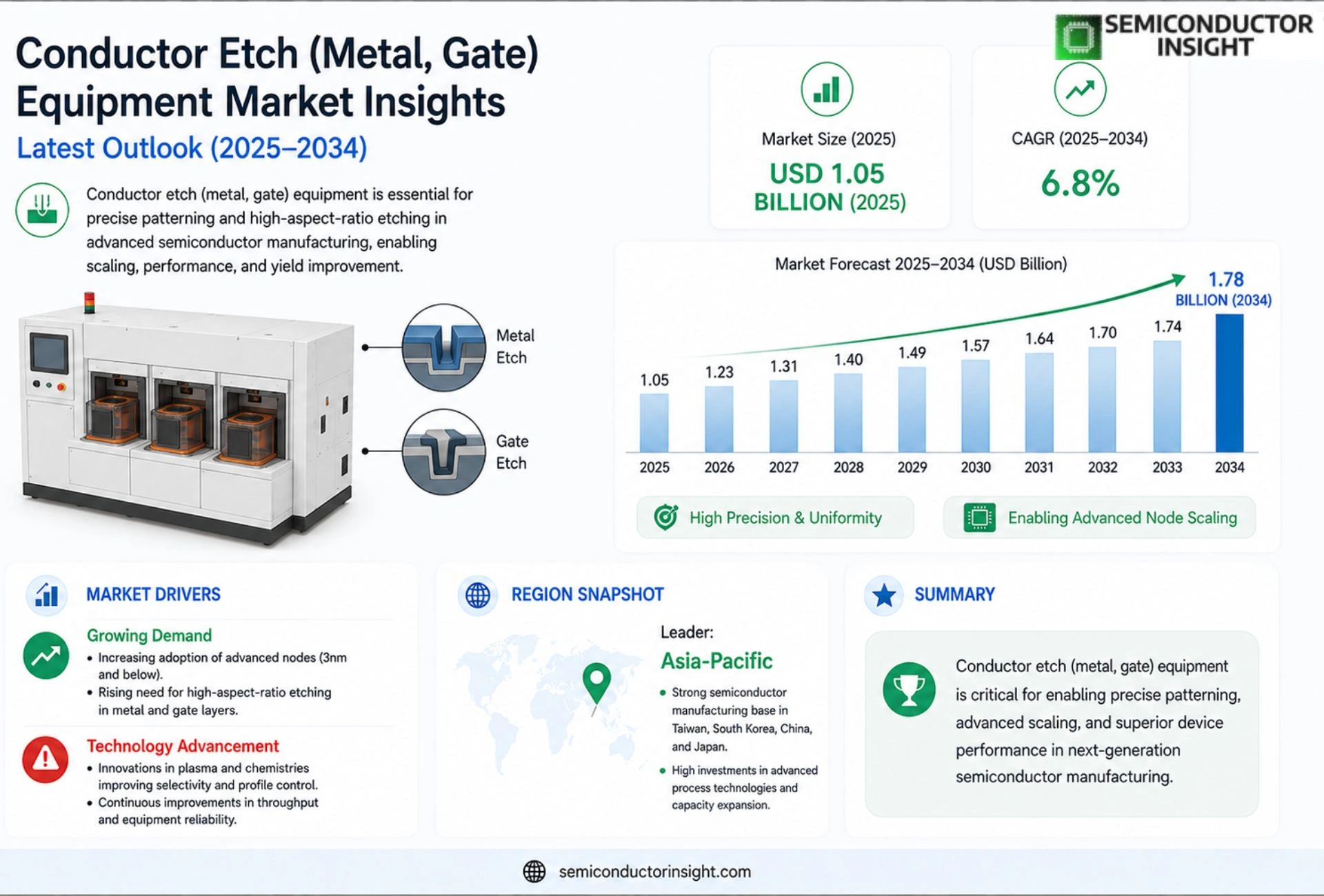
Global Conductor Etch (Metal, Gate) Equipment Market size was valued at USD 1.05 billion in 2025. The market is projected to grow from USD 1.23 billion in 2026 to USD 1.78 billion by 2034, exhibiting a CAGR of 6.8% during the forecast period.
Conductor etch (metal, gate) equipment comprises precision plasma‑based tools that selectively remove metal layers and define gate structures on silicon wafers. These systems integrate advanced process control, high‑density plasma sources, and endpoint detection to enable sub‑10 nm node patterning while minimizing damage to underlying dielectric layers.
The market is accelerating because semiconductor manufacturers are scaling down device geometries, driving demand for finer metal interconnects and tighter gate profiles. Furthermore, the rollout of 5G infrastructure and emerging AI workloads increase wafer throughput requirements, prompting fabs to upgrade to higher‑productivity etch platforms. Key players such as Lam Research, Applied Materials, Tokyo Electron, and Hitachi High‑Technologies are expanding their portfolios through automation upgrades and collaborative R&D programs.
MARKET DRIVERS
Increasing Semiconductor R&D Expenditure
The rise in research and development budgets across leading semiconductor manufacturers is a primary catalyst for Conductor Etch (Metal, Gate) Equipment Market. Companies are allocating greater resources to advanced node development, which directly boosts demand for high‑precision etch tools capable of handling sub‑10 nm metal and gate patterns.
Shift Toward 3D Integration Technologies
Emerging 3D stacking and heterogeneous integration architectures require more aggressive etching processes to achieve vertical interconnects without compromising critical dimensions. This technological shift is expanding the addressable market for etch equipment that delivers uniformity across complex topographies.
➤ “Improved plasma control and real‑time endpoint detection are accelerating adoption of next‑generation etch platforms.”
Manufacturers are also responding to tighter environmental regulations by investing in equipment with reduced chemical waste and higher throughput, further reinforcing growth momentum Conductor Etch (Metal, Gate) Equipment Market.
MARKET CHALLENGES
Complex Process Integration
Integrating metal and gate etch steps within a single manufacturing flow introduces significant process control challenges. Variations in etch selectivity and profile control can lead to yield losses, making equipment reliability a critical concern for fabs.
Other Challenges
Cost Volatility
The capital intensity of advanced etch systems, combined with fluctuating material prices, creates budgeting uncertainty for both established fabs and emerging players.
MARKET RESTRAINTS
Stringent Cleanroom Standards
Compliance with ultra‑cleanroom classifications demands additional investments in contamination control and validation protocols. These requirements can lengthen equipment qualification cycles and delay adoption of new etch technologies.
MARKET OPPORTUNITIES
Emerging AI‑Driven Process Optimization
The integration of artificial intelligence and machine learning into etch process monitoring offers prospects for predictive maintenance, adaptive recipe tuning, and yield enhancement. Companies that embed AI capabilities into their platforms are poised to capture a growing share of Conductor Etch (Metal, Gate) Equipment Market.
Trends
Scaling Down Device Geometries Accelerates Market Momentum
The continued push toward sub‑10 nm nodes is compelling semiconductor fabs to adopt more precise conductor etch (metal, gate) equipment. Advanced plasma sources and high‑density ion generation enable selective removal of metal layers while preserving delicate dielectric structures. As manufacturers target tighter gate profiles for 5G and AI‑driven workloads, throughput requirements rise, prompting investment in next‑generation etch platforms that deliver higher etch rates with reduced defectivity. The convergence of device scaling and performance‑critical applications is therefore a primary catalyst shaping market direction.
Other Trends
Automation and Integrated Process Control
Leading vendors are embedding real‑time endpoint detection and closed‑loop feedback into their systems, reducing cycle time and operator intervention. Automation frameworks link etch tools with lithography and metrology modules, creating a streamlined workflow that enhances yield consistency across high‑volume production lines. These capabilities are especially valuable for fabs seeking to minimize variation as feature sizes shrink, and they represent a notable shift from manual tuning to data‑driven process optimization.
Competitive Landscape and Innovation Pathways
Key players such as Lam Research, Applied Materials, Tokyo Electron, and Hitachi High‑Technologies are expanding portfolios through portfolio diversification and strategic R&D collaborations. Recent product releases focus on modular architecture, allowing customers to upgrade plasma generators and control electronics without full equipment replacement. This modular approach aligns with the industry’s demand for flexible capital expenditure and supports rapid adoption of emerging process nodes. Competitive pressure is driving faster innovation cycles, resulting in broader feature sets and improved energy efficiency across the equipment spectrum.
COMPETITIVE LANDSCAPE
Key Industry Players
Conductor Etch (Metal, Gate) Equipment Market Competitive Overview
Conductor Etch (Metal, Gate) Equipment Market is dominated by a handful of global semiconductor capital equipment manufacturers that control the majority of revenue streams and technology roadmaps. Lam Research and Applied Materials together account for roughly 45 % of the 2025 market value, leveraging their extensive product portfolios that span high‑density plasma (HDP) and atomic layer etch (ALE) platforms. Tokyo Electron and Hitachi High‑Technologies follow as the next tier, offering differentiated plasma sources and integrated endpoint detection that cater to sub‑10 nm node requirements. These leaders benefit from deep R&D pipelines, strategic fab partnerships, and recurring upgrade contracts, creating a consolidated market structure where scale and innovation act as primary barriers to entry.
Beyond the top tier, a cohort of specialized players contributes niche capabilities that enhance process flexibility and cost efficiency. SCREEN Semiconductor Solutions focuses on high‑throughput batch tools for mature nodes, while Nordson Medialine supplies precision plasma generators for thin‑film gate etching. Plasma‑Therm (now part of MKS Instruments) and MKS Instruments provide modular RF and vacuum solutions that are often integrated into larger system builds. Companies such as SENTECH, SIMTEC, and Dyade deliver region‑specific service and customization, allowing smaller fabs to adopt advanced etch chemistries without the full capital outlay of the leading OEMs. This tiered ecosystem sustains competitive pressure by driving incremental innovation, price competition, and localized support across the global semiconductor landscape.
List of Key Conductor Etch (Metal, Gate) Equipment Companies Profiled
- Lam Research
- Applied Materials
- Tokyo Electron
- Hitachi High‑Technologies
- SCREEN Semiconductor Solutions
- Nordson Medialine
- Plasma‑Therm
- MKS Instruments
- SENTECH
- SIMTEC
- Dyade
- UltraClean Systems
- ASML (process integration services)
- KLA Corporation (metrology integration)
- Tokyo Electron Device
Segment Analysis:
| Segment Category | Sub-Segments | Key Insights |
| By Type |
|
Single‑Wafer Etch Systems
|
| By Application |
|
Gate Stack Formation
|
| By End User |
|
Foundries
|
| By Technology Platform |
|
Inductively Coupled Plasma
|
| By Integration Level |
|
Cluster Tool Integration
|
Regional Analysis:
United States
Strong government support for semiconductor manufacturing, growing demand for advanced microprocessors and memory chips, increasing adoption of advanced packaging technologies.
Development of EUV lithography and its impact on etching processes, increasing adoption of plasma-enhanced chemical vapor deposition (PECVD) and atomic layer deposition (ALD).
Dominated by a few major international players, with increasing competition from domestic manufacturers focusing on niche applications and cost-effective solutions.
Continued growth expected driven by the increasing complexity of semiconductor devices and the expansion of end-use industries like automotive and industrial electronics.
Europe
Europe exhibits a steady and specialized demand for Conductor Etch (Metal, Gate) Equipment. The region’s strength lies in its established presence of advanced semiconductor manufacturers, particularly in countries like Germany, France, and the Netherlands. A focus on high-performance computing, automotive electronics, and industrial applications drives the need for precise and reliable etching solutions for intricate chip structures. European companies are increasingly emphasizing energy-efficient and environmentally friendly equipment, aligning with stringent regulatory standards. Collaboration between research institutions and industry players fosters innovation in process development and equipment design to meet the evolving demands of the market. The market is characterized by a strong emphasis on quality and reliability.
Asia-Pacific
Asia-Pacific is the largest and fastest-growing market for Conductor Etch (Metal, Gate) Equipment. Driven by the dominance of semiconductor manufacturing hubs like Taiwan, South Korea, and China, the region accounts for a significant share of global demand. The proliferation of smartphone production, consumer electronics, and the burgeoning electric vehicle (EV) industry fuels the need for advanced etching technologies. Significant investments in expanding semiconductor fabrication capacity are further boosting market growth. While cost competitiveness is a key factor, there is also a growing demand for high-performance equipment to support the production of advanced nodes. The region is witnessing a rise in domestic equipment manufacturers, contributing to increased competition and innovation.
South America
South America represents a relatively smaller but growing market for Conductor Etch (Metal, Gate) Equipment. Demand is primarily driven by the expansion of electronics manufacturing and the increasing adoption of technology across various industries. The growing automotive sector and the development of local semiconductor capabilities contribute to the market’s prospects. While the market size is smaller compared to other regions, there is potential for growth as the electronics industry continues to evolve. Investment in infrastructure and technological advancements is expected to further fuel market expansion.
Middle East & Africa
The Middle East & Africa region is an emerging market for Conductor Etch (Metal, Gate) Equipment, with growth driven by increasing investments in technology and infrastructure development. The expansion of electronics manufacturing and the growing adoption of smart city initiatives are creating demand for advanced etching solutions. The region’s focus on diversifying its economy and developing local manufacturing capabilities is expected to further boost market growth. While the current market size is relatively small, the long-term outlook is promising, particularly with increasing government initiatives to promote technological advancements.
Report Scope
This market research report provides a comprehensive analysis of the Conductor Etch (Metal, Gate) Equipment Market , covering the forecast period 2026–2034. It offers detailed insights into market dynamics, technological advancements, competitive landscape, and key trends shaping the industry.
Key focus areas of the report include:
- Market Overview: The report begins with an overview outlining its current market scenario, key growth indicators, and industry transformation drivers. It discusses macroeconomic factors, demand–supply balance, regulatory landscape, and the strategic role of semiconductors in powering advancements across industries such as automotive, telecommunications, consumer electronics, and industrial automation.
- Market Size & Forecast: Historical data and future projections for revenue, unit shipments, and market value across major regions and segments.
- Segmentation Analysis: Detailed breakdown by product type, technology, application, and end-user industry to identify high-growth segments and investment opportunities.
- Regional Insights: Insights into market performance across North America, Europe, Asia-Pacific, Latin America, and the Middle East & Africa, including country-level analysis where relevant.
- Competitive Landscape: Profiles of leading market participants, including their product offerings, R&D focus, manufacturing capacity, pricing strategies, and recent developments such as mergers, acquisitions, and partnerships.
- Technology Trends & Innovation: Assessment of emerging technologies, integration of AI/IoT, semiconductor design trends, fabrication techniques, and evolving industry standards.
- Market Drivers & Restraints: Evaluation of factors driving market growth along with challenges, supply chain constraints, regulatory issues, and market-entry barriers.
- Stakeholder Insights: Insights for component suppliers, OEMs, system integrators, investors, and policymakers regarding the evolving ecosystem and strategic opportunities.
Primary and secondary research methods are employed, including interviews with industry experts, data from verified sources, and real-time market intelligence to ensure the accuracy and reliability of the insights presented.
FREQUENTLY ASKED QUESTIONS:
What is the current market size of Conductor Etch (Metal, Gate) Equipment Market?
-> Conductor Etch (Metal, Gate) Equipment Market size was valued at USD 1.05 billion in 2025. The market is projected to grow from USD 1.23 billion in 2026 to USD 1.78 billion by 2034, exhibiting a CAGR of 6.8% during the forecast period.
Which key companies operate Conductor Etch (Metal, Gate) Equipment Market?
-> Key players include Lam Research, Applied Materials, Tokyo Electron, Hitachi High‑Technologies, among others.
What are the key growth drivers?
-> Key growth drivers include technology node scaling, 5G infrastructure rollout, emerging AI workloads, and the demand for higher‑productivity etch platforms.
Which region dominates the market?
-> Asia‑Pacific is the fastest‑growing region, while North America remains a dominant market.
What are the emerging trends?
-> Emerging trends include automation upgrades, AI‑driven process control, and collaborative R&D programs.

Get Sample Report PDF for Exclusive Insights
Report Sample Includes
- Table of Contents
- List of Tables & Figures
- Charts, Research Methodology, and more...
 Download Sample Report PDF

