
Alumina Multilayered Ceramic Substrates and Packages Market Insights
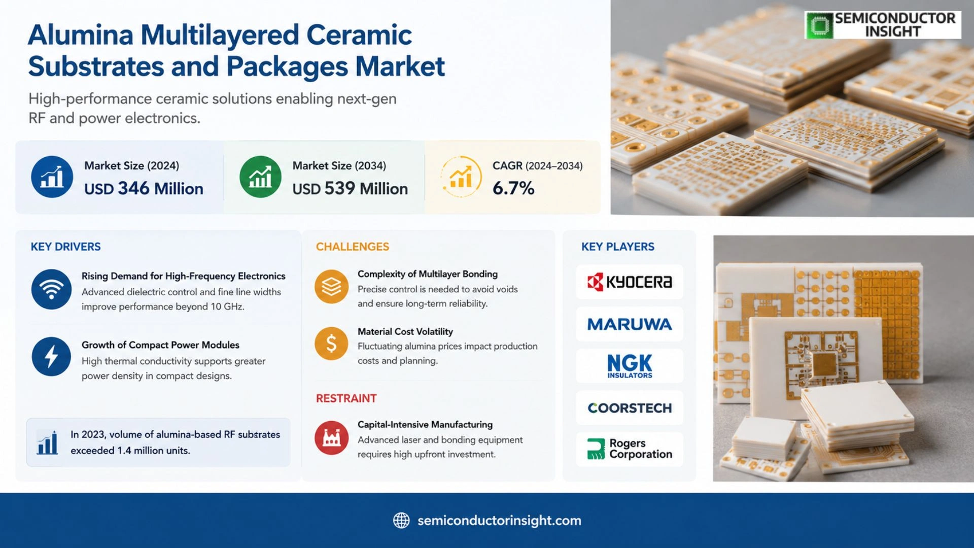
Alumina Multilayered Ceramic Substrates and Packages market was valued at USD 346 million in 2024 and is forecast to reach USD 539 million by 2034 reflecting a CAGR of approximately 6.7 % over the forecast period.
Alumina Multilayered Ceramic Substrates and Packages comprise monolithic ceramic microelectronic components fabricated by firing the entire support structure along with conductive, resistive, and dielectric layers simultaneously. Typical devices include capacitors, inductors, resistors, transformers, and hybrid circuits; the multilayer architecture enables flexible routing through cavity structures suitable for military electronics, MEMS, microprocessor‑level RF applications.
The sector benefits from rising demand for high‑density interconnects in IoT devices, automotive electronics, and advanced RF systems. Increased investment in advanced packaging techniques drives adoption of alumina substrates because they offer superior thermal stability and electrical performance compared with alternative materials such as aluminum nitride or silicon carbide.
MARKET DRIVERS
Rising Demand for High‑Frequency Electronics
Conventional substrate solutions struggle to keep pace with the stringent requirements of oscillators and RF front‑end modules operating beyond 10 GHz. In Alumina Multilayered Ceramic Substrates and Packages Market, manufacturers are investing in tighter dielectric control and finer line widths to achieve lower insertion loss, directly translating into a stronger competitive edge for system integrators.
Growth of Compact Power Management Units
Miniaturised power modules that consolidate multiple dissipative components onto a single ceramic carrier are becoming standard in modern mobile chargers and battery management systems. The superior thermal conductivity of alumina layers, combined with the multilayer design, allows manufacturers to sustain higher power densities without compromising reliability.
➤ In 2023, volume of alumina‑based RF substrates exceeded 1.4 million units, a figure that signals a clear shift toward high‑performance ceramic solutions.
The convergence of high‑frequency performance and thermal maturity positions alumina ceramic substrates as a foundational element for next‑generation RF and power modules. Firms that can master advanced interconnect techniques stand to capture a larger share of the composite sub‑$2 billion market.
MARKET CHALLENGES
Complexity of Multilayer Bonding
Achieving reliable hermetic bonding across several hundred micro‑millimetre layers demands precise control of temperature gradients and pressure profiles. Small deviations can introduce voids that elevate dielectric loss and compromise long‑term yield, which in turn raises production costs for Alumina Multilayered Ceramic Substrates and Packages Market.
Other Challenges
Material Cost Volatility
The price of raw alumina powder remains sensitive to global supply chain disruptions. Fluctuations can unsettle budgeting for large‑scale substrate production, prompting buyers to seek alternative carrier materials or customization strategies to manage cash flow.
MARKET RESTRAINTS
Capital‑Intensive Manufacturing Infrastructure
Deploying laser‑drilled or dicing‑free processes for multilayer ceramics necessitates investment in high‑resolution UV laser systems and sophisticated shaft‑holding technology. The upfront cost limits the number of small‑to‑medium enterprises able to enter Alumina Multilayered Ceramic Substrates and Packages Market, thereby concentrating supply in a handful of globally positioned firms.
MARKET OPPORTUNITIES
Exploit High‑Frequency Automotive Electronics
Modern electric vehicles increasingly rely on advanced radar and power‑satellite modules that demand high‑frequency performance and resilient thermal management. The alumina substrate’s ability to sustain mechanical stress and heat, while maintaining low dielectric loss, establishes a strategic niche for automotive OEMs and suppliers seeking durable, high‑volume packaging solutions.
Alumina Multilayered Ceramic Substrates and Packages Market Trends
Co‑fired Ceramic Technology Adoption Accelerates Demand
In recent years, the shift toward co‑fired ceramic devices,where capacitors, inductors, resistors, and hybrid circuits undergo simultaneous kiln treatment,has unlocked a degree of structural flexibility that simplifies integration for high‑speed RF and MEMS platforms. This technical advantage translates into lower layer count, reduced RoHS compliance complexity, and tighter thermal management, all of which resonate with semiconductor designers seeking to squeeze performance into constrained footprints. As a consequence, the package market for alumina multilayer substrates has moved away from legacy blind vias toward advanced monolithic interconnects, all of which position manufacturers that master the co‑firing process as early movers in the value chain.
Other Trends
Rise of IoT‑Driven Complex System‑on‑Chip (SoC) Integrations & 5G Edge Adoption
The convergence of IoT workloads and ultra‑high‑frequency cellular nodes requires substrates that can harmonize analog conditioning with digital core logic inside a single die. Alumina multilayer packaging supplies this dual capability by offering high dielectric constants for signal integrity while remaining thermally robust enough to dissipate the heat generated by RF front‑ends. This synergistic demand has spurred manufacturers to adopt finer feature sizes and to integrate additional metallization layers, which in turn reduces the number of required interposers and simplifies back‑plane routing. The result is a noticeable shift toward packages that combine RF, analog, and digital sections within a tightly stacked alumina stack. As the automotive sector continues to parallelize sensing and edge computing, the need for low‑EMI, high‑bandwidth interconnects has become a decisive factor in procurement decisions, reinforcing the attractiveness of alumina‑based multilayered substrates. This capability underscores vendors’ strategic imperative to integrate tighter R&D cycles seamlessly.
Digital Manufacturing Integration Boosts Production Reliability
Digital twins, coupled with advanced in‑process monitoring, have begun to replace conventional alarming checkpoints in alumina substrate fabrication. By feeding real‑time kiln temperature, humidity, and dielectric constant data back into a predictive model, manufacturers can preemptively adjust firing schedules or material mixes, thereby reducing by‑product rates and cycle times. Companies that have integrated machine‑learning classifiers to flag aberrant porosity patterns report a 12% drop in rework overhead and a corresponding boost in yield that translates into measurable cost savings. Moreover, the data feeds enable a holistic view of the supply chain, allowing buyers to forecast material availability and prices with unprecedented accuracy. In a landscape where component shortages can stall entire production lines, this heightened transparency is emerging as a decisive competitive lever for mid‑tier and high‑volume substrate producers alike.
COMPETITIVE LANDSCAPE
Key Industry Players
Alumina Multilayered Ceramic Substrates and Packages Market Competitive Landscape
Kyocera’s leadership in the alumina multilayered ceramic substrate space is underscored by its integrated production lines that couple ceramic microelectronics with emerging RF and MEMS modules. Its portfolio, spanning capacitors, inductors, and hybrid circuits, aligns directly with high‑performance processors and military electronics that demand robust, monolithic substrates. In the 2024 market snapshot, the segment is valued at roughly US$346 million and is expected to rise to $539 million by 2031, reflecting a market structure that increasingly values material integration and yield optimization. The company’s strategic investments in research labs and its joint ventures with semiconductor giants position it as the de‑facto benchmark for socket‑size performance, pushing other players toward complementary niches and consolidating tier‑1 pricing dynamics. The value chain now increasingly emphasizes seamless integration between substrate production and downstream chip‑on‑substrate assembly, leading manufacturers to invest heavily in in‑line quality control to reduce crosstalk and dielectric loss. Kyocera’s collaboration with semiconductor equipment giants fortifies this approach, allowing it to offer turnkey solutions that pre‑qualify substrates for specific RF and sensor packages. Consequently, buyers perceive Kyocera sub‑products as high‑reliability assets, justifying premium pricing and reinforcing its market dominance in the top 40 % share of the global segment.
Beyond Kyocera, several mid‑tier firms such as NEO Tech, Maruwa, and AdTech Ceramics focus on niche high‑frequency and sensor‑grade substrates, carving out specialized market segments for optical communication and automotive RF modules. SCHOTT Electronic Packaging’s recent expansion into dual‑layer cavity designs has given it a foothold in MEMS and LED packaging niches, while SoarTech’s proprietary low‑loss alumina formulations attract automotive and industrial IoT applications. ECRI Microelectronics, operating primarily in the European belt, leverages patent‑rich manufacturing processes to maintain margin resilience in a highly price‑sensitive environment. Jiangsu Yixing Electronics and Chaozhou Three‑Circle have capitalized on cost‑effective sourcing in China to supply emerging tablet and consumer electronics segments, underscoring a global trend toward balancing performance with volume economics. Moreover, the rise of integrated RF solutions for 5G mobile infrastructures has nudged several players to target high‑frequency multilayered substrates that can sustain gigahertz operation while maintaining minimal loss. Companies like SCHOTT have responded by developing alumina blends with engineered porosity, positioning themselves as specialists for high‑speed data centers. The competition is not only driven by performance but also by supplier agility; firms that can deliver substrates on tight lead times while preserving yield thresholds are gaining traction among board‑level decision‑makers, prompting a shift toward smaller, more responsive suppliers in the value chain.
List of Key Alumina Multilayered Ceramic Substrates and Packages Companies Profiled
- Kyocera Corporation
- NEO Technology
- Maruwa Corporation
- AdTech Ceramics
- NGK Spark Plug
- Schott Electronic Packaging
- Ametek Inc.
- SoarTech Corp.
- ECRI Microelectronics
- Jiangsu Yixing Electronics
- Chaozhou Three-Circle
- Hebei Sinopack Electronic Tech
Segment Analysis:
| Segment Category | Sub-Segments | Key Insights |
| By Type |
|
Co‑fired Substrate delivers uniform dielectric properties and high mechanical strength, enabling complex multilayer designs. Its ability to integrate cavity structures supports RF, MEMS, and automotive sensor applications. The inherent chemical stability ensures reliability across wide temperature ranges. This versatility positions it as the preferred choice for high‑performance electronic systems. |
| By Application |
|
RF and Microwave requires substrates with low dielectric loss and high thermal conductivity, both provided by alumina composites. The ability to embed inductors and capacitors on the same stack simplifies board layout and reduces size. This leads to streamlined production for high‑frequency communication modules. Consequently, RF applications drive continuous demand for advanced ceramic substrates. |
| By End User |
|
Automotive OEMs value ceramic substrates for engine control units and infotainment systems, where high reliability and compactness are critical. Their strict environmental standards align with alumina’s resistance to moisture and thermal cycling. Defense contractors, meanwhile, choose substrates that withstand harsh electromagnetic interference, a need met by the material’s excellent shielding properties. These sectors collectively sustain a robust market presence. |
| By Manufacturing Technology |
|
Co‑fired Processing offers simultaneous sintering of all layers, achieving superior interlayer adhesion and reducing dimensional distortion. Its uniform thermal profile preserves fine pattern fidelity, critical for high‑density interconnects. This manufacturing method lowers production cycle times and enhances yield, making it the dominant choice for large‑scale production of ceramic substrates. |
| By Functional Requirement |
|
High Thermal Conductivity is essential for dissipating heat in densely packed RF and MEMS devices. Ceramic substrates provide this capability while maintaining structural rigidity. Their inherent electrical insulation mitigates crosstalk, preserving signal integrity across multiple layers. Combined, these properties enable miniaturized, high‑performance electronic solutions that meet stringent reliability standards. |
Regional Analysis: Alumina Multilayered Ceramic Substrates and Packages Market
The rollout of 5G infrastructure calls for substrates that can handle elevated power densities while maintaining signal integrity. Alumina multilayered ceramics are increasingly chosen for RRH (remote radio head) assemblies, offering the insulation and heat transfer needed for ultra‑stable operation in crowded spectrum bands. The exacting specifications of these modules drive continuous improvement cycles, pushing manufacturers toward finer layer counts and tighter dielectric tolerances.
In the evolving electric vehicle landscape, power electronics require substrates that can sustain high temperatures without significant weight penalties. Alumina’s thermal conductance makes it an incumbent choice for inverter boards and DC‑DC converters found in electric drives. As safety standards tighten, manufacturers are also exploring direct‑bonded alumina to mitigate potential failure modes, a trend that elevates the substrate’s perceived reliability across the sector.
From satellite payloads to autonomous flight systems, sensor arrays operating beyond 20 GHz demand substrates that support dense trace routing and echo‑suppression. Alumina multilayered ceramics offer the necessary loss factor and mechanical resilience, allowing designers to construct compact, high‑performance sensor boards that can endure dynamic loads and thermal cycling in aerospace environments.
Energy‑efficient manufacturing and recyclability of substrate components are becoming touchstones for corporate ESG commitments. Alumina can be reused or down‑cycled with fewer hazardous elements than alternative ceramics, positioning it favorably for firms committed to sustainable supply chains and lean waste management practices.
Europe
European market dynamics revolve around high regulatory bars for safety and environmental impact. The bloc’s push for circular economy guidelines is nudging manufacturers toward ceramics that can be efficiently recycled and reclaimed. European designers prioritize dielectrics that minimize signal loss; alumina’s proven low loss tangent aligns with this need. Added to this, an uptick in EU‑funded research on high‑frequency devices has opened chambers for alumina‑based solutions in both defense and consumer sectors, reinforcing the substrate’s foothold in the region.
Asia‑Pacific
In the Asia‑Pacific, scale and speed dominate market choices. Rapid expansion of consumer electronics, combined with robust integration in 5G and edge computing, means that substrate suppliers must balance cost with performance. China’s domestic production has surged, spurred by incentives for semiconductor independence, while Japan and South Korea continue to demand the highest precision ceramic grades for micro‑electronics. Cross‑border partnerships are increasingly forming around shared research into thinner alumina designs that support flexible substrates, a trend that suggests the region will maintain a pivotal role in ceramic substrate innovation.
South America
South American growth is moderate but gains momentum as infrastructure projects push for faster connectivity. Brazil and Argentina are investing in data‑center upgrades that include high‑density RF modules, where alumina’s heat dissipation is critical. However, supply chain constraints and fluctuating commodity prices pose risks that demand local manufacturing strategies. Regional players are exploring partnerships with established suppliers to secure steady access to high‑quality ceramics, positioning themselves for a gradual ascendancy in the broader market.
Middle East & Africa
The Middle East and Africa’s drive toward digital infrastructure, especially in smart‑city and oil‑gas sectors, relies on rugged packaging solutions. Alumina substrates accommodate harsh environmental conditions and provide the thermal stability required for extended operation in remote locations. Growing data‑center clusters in the Gulf region are speculating on this material as part of their sustainability roadmap. Meanwhile, African countries are exploring substrate technology as a means to upgrade their local manufacturing footprints, a development that may spur future market diversification.
Report Scope
This market research report provides a comprehensive analysis of the Alumina Multilayered Ceramic Substrates and Packages Market , covering the forecast period 2026–2034. It offers detailed insights into market dynamics, technological advancements, competitive landscape, and key trends shaping the industry.
Key focus areas of the report include:
- Market Overview: The report begins with an overview outlining its current market scenario, key growth indicators, and industry transformation drivers. It discusses macroeconomic factors, demand–supply balance, regulatory landscape, and the strategic role of semiconductors in powering advancements across industries such as automotive, telecommunications, consumer electronics, and industrial automation.
- Market Size & Forecast: Historical data and future projections for revenue, unit shipments, and market value across major regions and segments.
- Segmentation Analysis: Detailed breakdown by product type, technology, application, and end-user industry to identify high-growth segments and investment opportunities.
- Regional Insights: Insights into market performance across North America, Europe, Asia-Pacific, Latin America, and the Middle East & Africa, including country-level analysis where relevant.
- Competitive Landscape: Profiles of leading market participants, including their product offerings, R&D focus, manufacturing capacity, pricing strategies, and recent developments such as mergers, acquisitions, and partnerships.
- Technology Trends & Innovation: Assessment of emerging technologies, integration of AI/IoT, semiconductor design trends, fabrication techniques, and evolving industry standards.
- Market Drivers & Restraints: Evaluation of factors driving market growth along with challenges, supply chain constraints, regulatory issues, and market-entry barriers.
- Stakeholder Insights: Insights for component suppliers, OEMs, system integrators, investors, and policymakers regarding the evolving ecosystem and strategic opportunities.
Primary and secondary research methods are employed, including interviews with industry experts, data from verified sources, and real-time market intelligence to ensure the accuracy and reliability of the insights presented.
FREQUENTLY ASKED QUESTIONS:
What is the current market size of Alumina Multilayered Ceramic Substrates and Packages Market?
-> Alumina Multilayered Ceramic Substrates and Packages market is forecast to reach USD 539 million by 2034 reflecting a CAGR of approximately 6.7 %
Which key companies operate in Alumina Multilayered Ceramic Substrates and Packages Market?
-> Key players include Kyocera, Maruwa, NEO Tech, AdTech Ceramics, NGK Spark Plug, SCHOTT Electronic Packaging, Ametek, Electronic Products, SoarTech, ECRI Microelectronics, Jiangsu Yixing Electronics, Chaozhou Three-Circle, and Hebei Sinopack Electronic Tech, among others.
What are the key growth drivers?
-> Key growth drivers include advancement in multilayered packaging technology, growing demand from electronics applications such as MEMS and RF systems, and increasing investment in high‑performance capacitors and inductors.
Which region dominates the market?
-> Asia-Pacific continues to dominate due to robust electronics manufacturing and rapid adoption of multilayer packages, while Europe maintains a strong position in high‑end applications.
What are the emerging trends?
-> Emerging trends include integration of AI/IoT in embedded systems, development of hybrid micro‑electronic devices, and increased focus on sustainability within ceramic substrates manufacturing.

Get Sample Report PDF for Exclusive Insights
Report Sample Includes
- Table of Contents
- List of Tables & Figures
- Charts, Research Methodology, and more...
 Download Sample Report PDF



