CMOS Digital Image Sensors Market Insights
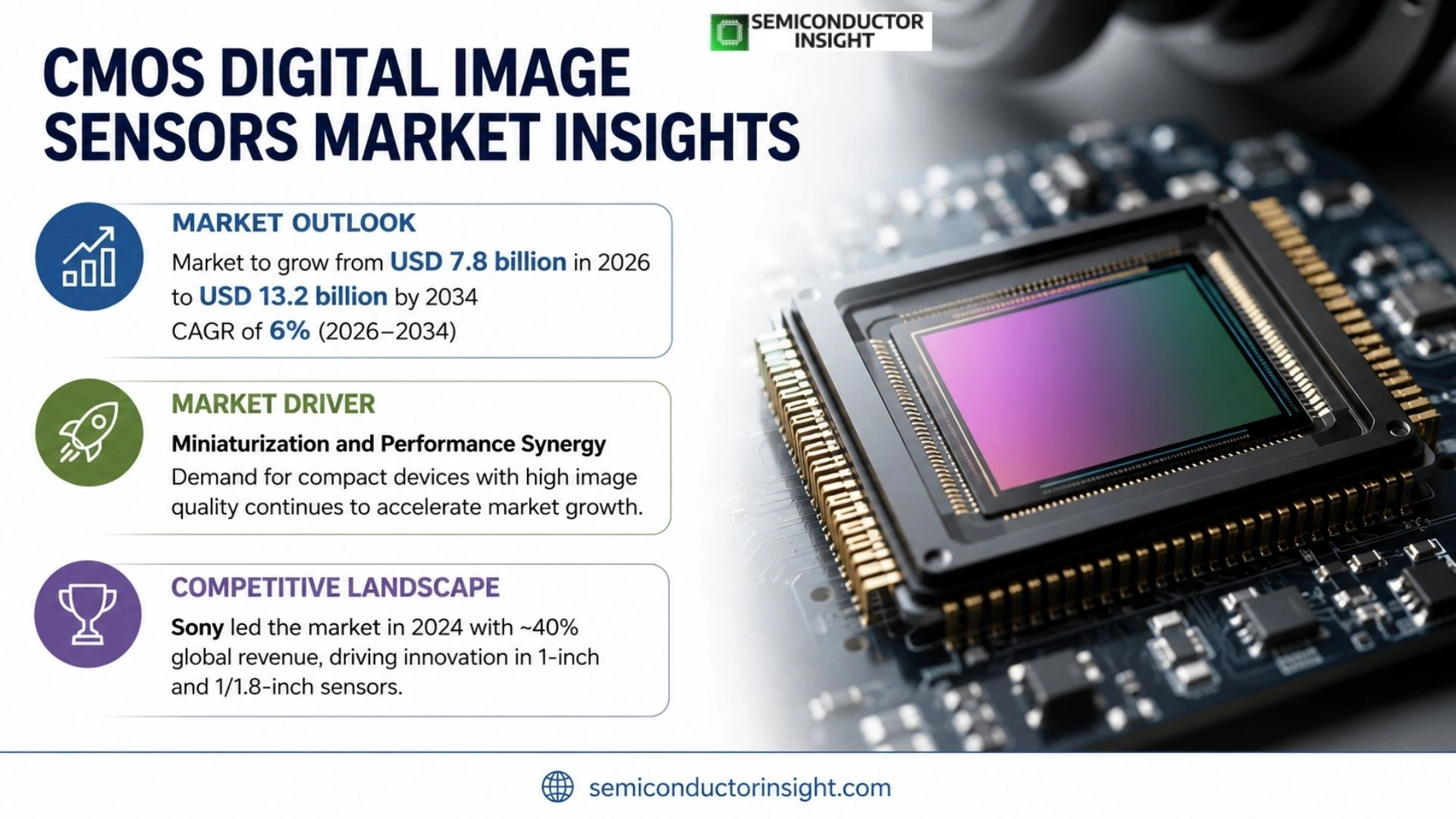
CMOS Digital Image Sensors market will rise from USD 7.8 billion in 2026 to USD 13.2 billion by 2034, registering a CAGR of 6% over the forecast period.
CMOS digital image sensors are semiconductor devices that convert incident light into electrical signals through complementary metal‑oxide‑semiconductor technology. They integrate photodiodes, analog front‑end circuitry and signal processing on a single silicon die, delivering low power consumption, high integration density and rapid readout speeds suited for smartphones, automotive cameras and industrial imaging applications.
MARKET DRIVERS
Miniaturization and Performance Synergy
The transition toward thinner, lighter devices has pushed CMOS Digital Image Sensors Market stakeholders to combine size reduction with uncompromised image fidelity. By shrinking sensor dimensions without sacrificing pixel pitch, manufacturers are now delivering sub–1‑millimeter‑wide cameras that maintain 12‑bit linearity and noise figures below 5 e⁻‑rms. This dual advantage translates directly into cost‑effective production lines, as fewer interconnects and simpler packaging reduce assembly time and material usage. For end users, the outcome is a surge of high‑resolution imaging solutions that fit inside wearable headsets, automotive dash‑cams, and factory inspection robots. The interplay between compact form factors and superior signal‑to‑noise ratios empowers companies to open margins in premium segments where image quality dictates pricing, thereby reshaping competitive dynamics across the value chain.
Advanced Applications Driving Adoption
The infiltration of CMOS sensors into originally niche verticals,such as autonomous vehicle perception, UAV surveillance, and minimally invasive medical imaging,constitutes a powerful growth vector for the market. Automotive OEMs are now incorporating triple‑camera arrays that deliver 1080 p 120‑fps video streams, while drone operators rely on 4K‑capable sensors with built‑in optical image stabilization to maintain georeferenced footage accuracy. In medical practice, endoscopic and retinal imaging systems have integrated 20‑megapixel CMOS modules to provide surgeons with real‑time, high‑contrast visualization of micro‑vascular structures. The convergence of edge‑processing units with these sensors encourages deeper on‑device analytics, reducing bandwidth requirements and enabling rapid decision making. Consequently, suppliers exposing integrated sensor‑processor packages enjoy higher lock‑in ratios, and partners benefit from accelerated go‑to‑market cycles.
➤ Innovative packaging techniques are enabling higher power efficiency while maintaining compact form factors, thereby unlocking new use cases that were previously constrained by heat and size limitations.
Strategic implications for vendors are evident: companies that can operate at scale while delivering pixel‑level performance gains will control premium market shares. Firms focusing on system‑on‑chip collaborations can leverage cross‑industry certification programs, thereby mitigating integration risks for buyers. Moreover, the broadening application spectrum creates a diversified revenue stream, reducing dependence on any single vertical and allowing price differentiation based on delivered feature sets. Therefore, the focus on innovation in both sensor design and integration is not only a technological imperative but also a decisive commercial lever.
MARKET CHALLENGES
Material Cost Volatility and Supply Constraints
Fluctuations in raw‑silicon procurement costs and limited availability of high‑purity photolithography resists exert pressure on production margins across the sensor ecosystem. Escalating demand for advanced lithographic tools has pushed capital expenditures higher, creating bottlenecks where only large‑cap manufacturers can secure consistent supply. Furthermore, the intricate supply chain that includes rare‑earth elements for backside illumination (BSI) wafers introduces additional lead‑time uncertainty. These material dynamics render CMOS Digital Image Sensors Market susceptible to price swings that ripple through the procurement plans of OEMs, prompting them to lock in contracts long before substitute technologies mature. The uncertainty drives a cautious delivery approach, elongating product rollouts and compressing the competitive window for newly launched sensor variants.
Other Challenges
Regulatory and Certification Hurdles
Compliance with regional safety standards,such as ISO 26262 for automotive, FCC Part 15 for wireless transmission, and CE‑A for medical devices,demands extensive testing cycles. The cumulative duration of qualification programs can extend across 18–24 months, and any non‑compliance triggers costly redesigns. For international expansion, distributors must navigate divergent certification authorities, each necessitating tailored documentation and on‑site validation. Consequently, market entry timelines are stretched, and the cost of inclusion rises; early adopters who misjudge regulatory complexity often face supply disruptions that reverberate through their entire product assurance chain.
MARKET RESTRAINTS
Capital Intensity and Long Development Cycles
Manufacturing CMOS sensors demands significant upfront capital commitments, especially as feature‑size pushes below 28 nm into deep‑trench regimes. Achieving yield targets for such advanced nodes requires precision metrology suites that routinely exceed $50 million. When coupled with an expected 12–14 month cycle from design validation to volume production, the financial exposure is considerable. Smaller players confront a dilemma: underwriting these costs risks depleting liquid reserves, while delaying entry to capture emerging markets may grant competitors a first‑mover edge. Additionally, the intricate process control necessary to sustain <1% defect rates imposes a steep learning curve that only long‑line entrepreneurs with deep engineering ecosystems can master. Limited access to these capabilities curbs the pace at which the market can respond to volatile end‑user demand, thereby restricting overall demand elasticity across the sensor value network.
MARKET OPPORTUNITIES
Enterprise-Level Edge Computing Synergies
The rise of edge‑processing architectures,particularly in autonomous systems and industrial IoT,creates fertile ground for collaborative sensor‑processor ecosystems. By embedding low‑power neural inference engines directly onto the sensor die, manufacturers can deliver real‑time analytics such as anomaly detection, depth estimation, and intelligent situational awareness. This integration not only reduces data traffic from device to cloud but also eliminates backhaul latency, appealing to safety‑critical applications in aviation, defense, and chemical processing. From a revenue standpoint, such modular bundles position vendors uniquely in a market that seeks to minimize end‑to‑end solution architecture complexity. Enterprise buyers are increasingly willing to pay a premium for integrated solutions that promise faster deployment and reduced operational footprint, thereby unlocking new economic tiers for CMOS Digital Image Sensors Market.
Another avenue of expansion lies in the adaptation of micro‑LED illumination arrays that pair with standard CMOS chips for mixed‑signal capture. This synergy offers unprecedented control over exposure and depth‑of‑field while maintaining standard sensor production flows. The resulting product portfolio addresses a growing demand for immersive imaging in augmented reality devices and compact cinematographic rigs. By tapping into these convergent technologies, suppliers can diversify revenue streams, counterbalance the anti‑seasonality of traditional camera markets, and establish forward‑looking partnerships with content creation platforms that value plug‑and‑play sensor modules.
CMOS Digital Image Sensors Market Trends
Sub‑Micron Pixel Architecture as the New Competitive Lever
CMOS digital image sensor landscape is undergoing a layered evolution, with technical leap and application focus intertwining. Recent process refinements, edge‑centric logic, and on‑sensor intelligence converge to produce devices that are faster, slimmer, and more adaptable across automotive, security, and industrial sectors. Their enhanced light sensitivity and reduced form factor open new commercial avenues for companies targeting integrated vehicle cockpit systems.
The recent pivot toward sub‑micron pixel layouts is reshaping the competitive fabric. By slicing pixel footprints while adding within‑pixel circuitry,noise reducers, brief exposure controls, and binning options,manufacturers elevate quantum efficiency and low‑light fidelity. This advancement fuels code‑breaking image resolutions that premium automotive and consumer cameras tout. Simultaneously, the associated lithographic leap increases capital demand, but the payoff is a sharper market edge for firms that master the process migration. The change also impacts sensor packaging and yields, because smaller pixel integration compels new die‑level cooling strategies.
Other Trends
Rise of Edge‑Computing Enabled Sensors
Edge‑computing sensors embed data‑compression cores and programmable logic to cut raw throughput by up to three times. The bandwidth savings enable seamless deployment in autonomous platforms and industrial robots, where real‑time inference is critical. Lower latency also sharpens security surveillance, allowing immediate threat detection without external processors. The shift demands multi‑die packaging and higher logic densities, prompting fabs to adopt advanced EUV tools and tighter design rules to maintain yield. This integration also creates a tighter supply chain relationship between sensor and AI IP vendors, as firms collaborate to meet strict time‑to‑market targets.
Integration of AI Acceleration on the Sensor Die
Embedding AI accelerators directly onto the sensor die is now a differentiator. The on‑chip network processes classification and adaptive exposure during capture, slashing power draw and eliminating high‑speed bus dependencies. Battery‑operated cameras benefit from reduced data traffic, a critical win for satellite imaging and mobile devices. Companies crafting dedicated neural cores find a market niche, yet the added die area challenges cost and yield; nonetheless, successful pilots show that the performance lift offsets the incremental step‑rate. Partnerships with AI software firms help integrate machine‑learning pipelines, making the sensor an end‑to‑end solution for edge vision.
Taken together, these trajectories place the CMOS image sensor domain in transition from pixel‑centric to intelligence‑centric products. Firms that can navigate the process leap, secure EUV tooling, and embed AI logic will capture premium packaging, command higher margins, and secure market share in automotive safety, industrial inspection, and consumer drones. Stakeholders should evaluate supply‑chain resilience to advanced lithography nodes and forge alliances with both sensor and AI IP developers to stay ahead. Such partnerships should also address data‑security regulations, ensuring that on‑device processing complies with privacy standards in regulated markets.
COMPETITIVE LANDSCAPE
Key Industry Players
CMOS Digital Image Sensors Competitive Landscape Overview
Sony remains the benchmark in CMOS digital imaging, holding nearly 40% of global revenue in 2024 and spearheading the shift toward 1‑inch and 1/1.8‑inch sensors for automotive and high‑end mobile sectors. Its flagship 1.2‑megapixel sensor integrated with deep‑screen display technology drives premium smartphones and advanced driver‑assist systems. Samsung’s expansion into back‑side illumination (BSI) sensors has secured a complementary 12% share, thanks to its DRAM and memory synergy. Omnivision, with its compact 1/2.8‑inch modules, dominates the security‑monitoring niche, while its 3‑in‑chassis sensors open new avenues. The market structure reveals a handful of leading conglomerates controlling 75% of revenue, with the remaining tiers fragmented across small to mid‑sized firms catering to specialized verticals.
Galaxycore focuses on stacked‑pixel architectures that allow simultaneous light trapping and signal processing, positioning it to capture the emerging automotive radar‑machine‑vision segment. SK Hynix leverages its foundry capabilities to supply custom photodiode arrays for aerospace imaging. Onsemi’s emphasis on low‑power, linear CMOS chips serves the IoT and wearables markets, aligning with the forecasted penetration of smart homes. STMicro’s dual‑mode sensors combine standard imaging with infrared capabilities, evidence of cross‑technology convergence. Panasonic’s legacy in analog imaging has evolved into high‑resolution 60‑megapixel modules for industrial inspection. SamrtSens’ proprietary backside‑side illumination structure offers superior low‑light performance for security collections. Canon’s re‑entry into sensor manufacturing suggests a strategic pivot toward large‑format cameras, while SOI’s self‑organizing integrated circuits open novel calibration pathways. Collectively, these niche vendors form a tightly woven ecosystem that responds agilely to technical demands.
List of Key CMOS Digital Image Sensors Companies Profiled
- Sony
- Samsung
- Omnivision
- Galaxycore
- SK Hynix
- Onsemi
- STMicro
- Panasonic
- SamrtSens
- Canon
- SOI
- Fairchild Semiconductor
- Ilitec
Segment Analysis:
| Segment Category | Sub-Segments | Key Insights |
| By Type |
|
Backside‑Illuminated (BSI) offers key advantages: • Exceptional low‑light sensitivity critical for modern cameras. • Higher pixel density supports increased resolution without sacrificing performance. • Enables more compact sensor designs for slimmer devices. |
| By Application |
|
Smartphone dominates usage: • Market leaders prioritize high‑resolution and low‑light performance. • Integrated image signal processing drives fast frame rates. • Battery efficiency and form‑factor constraints shape sensor design. |
| By End User |
|
Consumer Electronics drives demand: • Personal devices seek lightweight and energy‑efficient solutions. • Rapid innovation cycles require flexible sensor families. • User expectations for image clarity and color fidelity remain high. |
| By Technology |
|
Edge Computing Sensor is gaining traction: • On‑sensor processing reduces data latency for real‑time applications. • Enables smart devices to operate autonomously. • Power budgets and connectivity requirements drive integration. |
| By Integration |
|
Embedded solutions dominate, especially in mobile and industrial gear: • Tight form‑factor and thermal constraints guide design. • Integration with processors enables advanced computational photography. • Manufacturers adopt modular sensor families for rapid deployment. |
Regional Analysis: CMOS Digital Image Sensors Market
Asia-Pacific
China’s sensor output is anchored by state‑backed industrial parks that cluster Tier‑1 suppliers and offer tax incentives for integrated chip fabrication. The domestic push for 5G and autonomous vehicles has spurred demand for high‑resolution, high‑frame‑rate CMOS modules, compelling firms to adopt silicon‑photonic integration. Recent collaborations between local OEMs and university research teams have accelerated prototype development cycles, positioning China as a primary supplier for mid‑tier smartphones and automotive camera units.
India’s growth is underpinned by a surge in maker‑culture initiatives and a thriving startup ecosystem that focuses on low‑cost, high‑penetration sensor solutions. Government incentives for ‘Make in India’ projects have catalyzed local fabrication of CMOS back‑side illumination chips, reducing import dependency. This trend serves the burgeoning mobile market and regional automotive segments targeting domestic manufacturing of autonomous features.
Japan’s strategic emphasis on precision engineering fuels its dominance in high‑performance sensors, particularly those used in machine vision and defense applications. Long‑standing partnerships with global equipment manufacturers allow Japanese firms to incorporate advanced lithography techniques, preserving a competitive edge in image‑quality metrics critical for industrial automation and medical diagnostics.
South Korea’s robust semiconductor infrastructure supports a vertically integrated supply chain, with its flagship conglomerates delivering state‑of‑the‑art CMOS sensors for consumer electronics and automotive lighting. The region’s focus on global‑shutter designs feeds the high‑speed imaging demands of automotive safety systems, ensuring continued relevance in competitive OEM negotiations.
North America
North America remains a critical contributor to CMOS Digital Image Sensors Market, largely through a concentration of design‑heavy OEMs and a vibrant startup ecosystem championing machine‑learning‑enabled imaging chips. While manufacturing capabilities have receded, the region’s expertise in algorithm‑centric sensor software ensures continued dominance in high‑end fields such as augmented reality, autonomous vehicle perception, and sophisticated surveillance systems. U.S. teams are rapidly prototyping sensors with integrated vision‑processing coprocessors, a development that promises to obviate costly external GPU requirements and accelerate product time‑to‑market for security and automotive firms. This strategic shift toward “smart sensors” signals a broader industry pivot where optical performance is coupled with edge‑AI capabilities, granting U.S. companies a qualitative edge over purely hardware‑centric competitors. The concomitant rise in semiconductor‑design‑as‑a‑service models further democratizes access to custom imaging solutions, enabling mid‑tier OEMs to tap into advanced technology without large upfront capital commitments.
Europe
Europe sustains a strong presence in CMOS Digital Image Sensors Market through its emphasis on regulatory compliance, data privacy, and environmental sustainability. Leading European firms are pioneering low‑power, high‑resolution sensors tailored for autonomous navigation and medical imaging, aligning with stringent CE and FDA standards. The region’s commitment to circular economy principles has spurred investment in post‑consumer recycling initiatives, thereby extending the lifecycle of sensor components. Additionally, European research consortia are driving breakthroughs in quantum imaging and multi‑spectral sensors, positioning the continent as an innovation hub for neuroprosthetic and defense applications. These advances reinforce Europe’s credibility as a source of high‑quality, reliable sensor technology that meets the stringent demands of regulated markets across the globe.
South America
South America’s influence on CMOS Digital Image Sensors Market is gradually expanding, propelled by a surge in domestic telecommunications infrastructure projects and a national push for tech self‑reliance. Emerging manufacturing nodes in Brazil and Chile are increasingly focused on producing mid‑tier sensor modules for smartphones and industrial automation, leveraging tax incentives and free‑trade agreements that reduce import costs. Moreover, the region’s growing agricultural monitoring sector is adopting high‑resolution imaging sensors for precision farming, fostering a niche market that supports rural employment and technology diffusion. However, fragmentation across national borders and variable regulatory frameworks present challenges that could dampen economies of scale unless a unified regional strategy materializes.
Middle East & Africa
In the Middle East and Africa, CMOS Digital Image Sensors Market is largely shaped by defense and aerospace contracts, where security and reliability dictate supplier selection. Nations within the GCC are investing heavily in satellite imaging and autonomous platform development, creating demand for rugged, high‑temperature climate‑resistant sensors. Additionally, the region’s expanding renewable energy sector is adopting imaging sensors for predictive maintenance of solar panels and wind turbines, a use case that promotes the deployment of low‑cost, high‑durability sensors. African markets are witnessing a nascent wave of mobile health initiatives that employ low‑cost image sensors to support telemedicine diagnostics, though capital constraints and infrastructural deficits remain significant hurdles for widespread adoption.
Report Scope
This market research report provides a comprehensive analysis of the CMOS Digital Image Sensors Market , covering the forecast period 2026–2034. It offers detailed insights into market dynamics, technological advancements, competitive landscape, and key trends shaping the industry.
Key focus areas of the report include:
- Market Overview: The report begins with an overview outlining its current market scenario, key growth indicators, and industry transformation drivers. It discusses macroeconomic factors, demand–supply balance, regulatory landscape, and the strategic role of semiconductors in powering advancements across industries such as automotive, telecommunications, consumer electronics, and industrial automation.
- Market Size & Forecast: Historical data and future projections for revenue, unit shipments, and market value across major regions and segments.
- Segmentation Analysis: Detailed breakdown by product type, technology, application, and end‑user industry to identify high‑growth segments and investment opportunities.
- Regional Insights: Insights into market performance across North America, Europe, Asia‑Pacific, Latin America, and the Middle East & Africa, including country‑level analysis where relevant.
- Competitive Landscape: Profiles of leading market participants, including their product offerings, R&D focus, manufacturing capacity, pricing strategies, and recent developments such as mergers, acquisitions, and partnerships.
- Technology Trends & Innovation: Assessment of emerging technologies, integration of AI/IoT, semiconductor design trends, fabrication techniques, and evolving industry standards.
- Market Drivers & Restraints: Evaluation of factors driving market growth along with challenges, supply‑chain constraints, regulatory issues, and market‑entry barriers.
- Stakeholder Insights: Insights for component suppliers, OEMs, system integrators, investors, and policymakers regarding the evolving ecosystem and strategic opportunities.
Primary and secondary research methods are employed, including interviews with industry experts, data from verified sources, and real‑time market intelligence to ensure the accuracy and reliability of the insights presented.
FREQUENTLY ASKED QUESTIONS:
What is the current market size of CMOS Digital Image Sensors Market?
-> CMOS Digital Image Sensors market will rise from USD 7.8 billion in 2026 to USD 13.2 billion by 2034, registering a CAGR of 6%
Which key companies operate in CMOS Digital Image Sensors Market?
-> Key players include Sony, Samsung, Omnivision, Galaxycore, SK Hynix, On Semi, ST Micro, Panasonic, SamrtSens, Canon, and SOI.
What is the estimated size of the U.S. market?
-> The U.S. market is estimated at USD 1,200 million in 2024.
What is the projected market size for China?
-> China is projected to reach USD 1,500 million by 2024.
What will the FSI segment grow to by 2031?
-> The FSI segment is forecast to reach USD 1,050 million by 2031, with a CAGR of 9.5% over the next six years.
What market share do the top five players hold in 2024?
-> In 2024, the global top five players had a share of approximately 70% in terms of revenue.
How has global revenue trended from 2020 to 2024?
-> Global revenue grew from USD 3,200 million in 2020 to USD 4,500 million in 2024, reflecting consistent annual growth.
What are the global sales volumes (K units) from 2020 to 2024?
-> Global sales increased from 520 K units in 2020 to 800 K units in 2024, indicating expanding demand.
What are the application segment percentages in 2024?
-> In 2024, the application segments were: Smartphone 35%, Security Monitoring 25%, Vehicle Electronics 20%, and Others 20%.
What are the type segment percentages in 2024?
-> In 2024, the type segments were: Front‑Side‑Illumination (FSI) 55% and Back‑Side‑Illumination (BSI) 45%.
What are the key drivers of market growth?
-> Key drivers include continuous innovation in sensor resolution, integration of AI/ML capabilities, increasing adoption in automotive and industrial sectors, and rising demand for high‑definition imaging across consumer electronics.

Get Sample Report PDF for Exclusive Insights
Report Sample Includes
- Table of Contents
- List of Tables & Figures
- Charts, Research Methodology, and more...
 Download Sample Report PDF