
Key Statistics
Key Takeaways
- TLC remains the volume anchor because it balances density, endurance and cost across enterprise, client and mobile storage, while QLC is gaining relevance where capacity economics outweigh write-endurance requirements.
- Enterprise SSDs are the strongest application engine as AI inference, cloud storage and data-intensive services lift requirements for high-capacity, power-efficient flash in data centers.
- 200+ layer architectures define the technology frontier. Samsung entered mass production with ninth-generation 1Tb TLC V-NAND in 2024, while SK hynix moved 321-layer 2Tb QLC into mass production in 2025.
- Asia Pacific is the largest supply-side market. SEMI projected Korea, China, Taiwan and Japan to account for 80% of global 300 mm front-end capacity in 2025, reinforcing the region’s leverage over memory manufacturing.
- Manufacturing complexity and memory-cycle economics remain the main constraints: higher stacks require tighter etch, deposition, bonding and yield control, while pricing swings can delay capacity additions even when bit demand expands.
3D NAND Flash Memory Market Overview
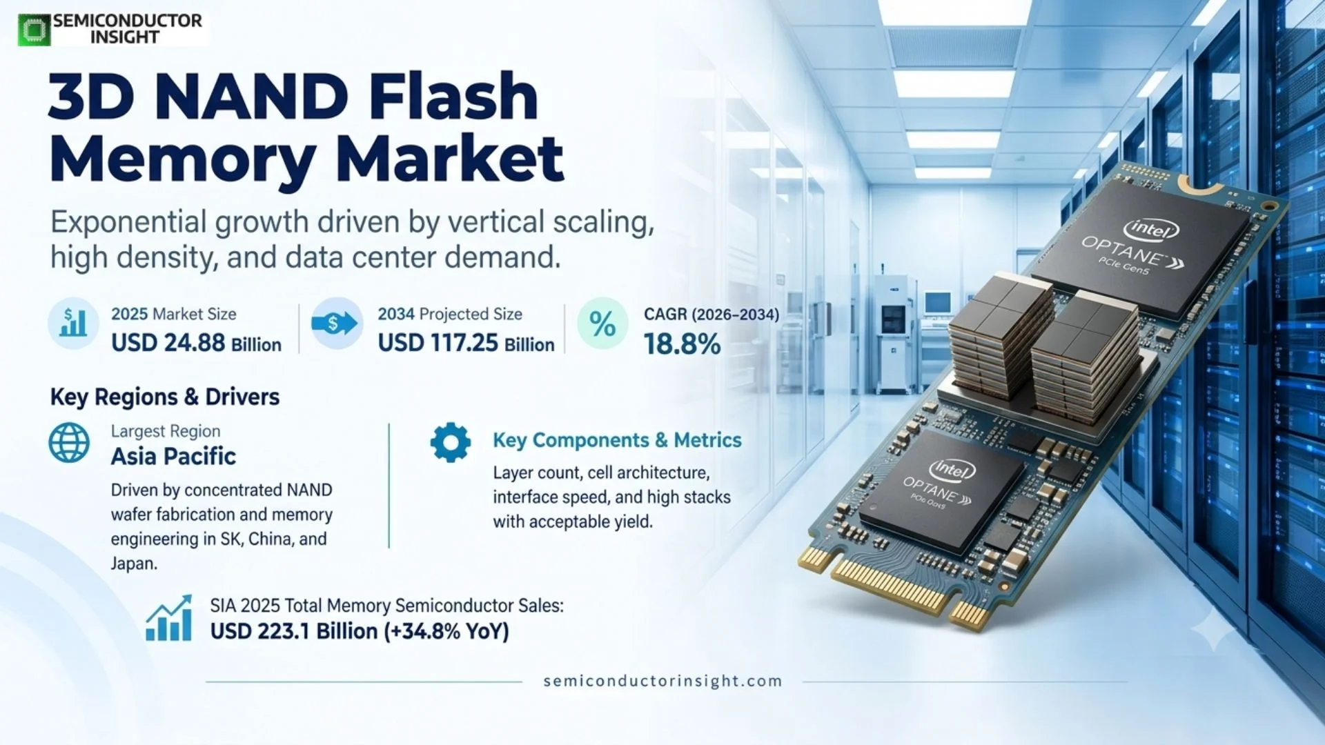
3D NAND Flash Memory Market was valued at USD 24.88 billion in 2025 and is projected to reach USD 117.25 billion by 2034, expanding at a 18.8% over 2026–2034. The 2026 market value is USD 29.55 billion. Asia Pacific represents the largest market in 2025, supported by the concentration of NAND wafer fabrication, memory engineering, equipment investment and device assembly across South Korea, China and Japan.
3D NAND is non-volatile flash memory built by stacking memory cells vertically rather than relying only on lateral transistor scaling. The architecture raises storage density per wafer and gives manufacturers a route to lower cost per bit while supporting high-capacity solid-state drives, embedded mobile storage and industrial devices. Commercial differentiation increasingly comes from layer count, cell architecture, interface speed, controller co-optimization, power efficiency and the ability to manufacture high stacks at acceptable yield.
The demand mechanism has shifted from consumer-device capacity alone toward a broader storage hierarchy shaped by AI and cloud computing. SIA reported memory semiconductor sales of USD 223.1 billion in 2025, up 34.8% year over year. Enterprise SSD suppliers are simultaneously introducing higher-capacity drives using newer NAND generations, linking bit growth to data-center rack density, energy efficiency and the amount of online data that AI workloads must store and retrieve.
Supply economics are equally important. SEMI projected installed 3D NAND capacity at 3.7 million 200 mm-equivalent wafers per month in 2025, while later equipment-spending plans placed 3D NAND investment at USD 56 billion over 2026–2028. That investment supports higher layer counts and new process steps, but it also raises the importance of utilization, yield learning and disciplined bit-supply growth when pricing conditions soften.
Segment Analysis: By Type
By type, the source-defined market is segmented into SLC, MLC, TLC and QLC. TLC holds the broadest commercial position because it spans enterprise, client and embedded storage, while QLC is the principal density-led growth vector for read-intensive and very-high-capacity applications. SLC and MLC remain relevant where endurance, deterministic performance or legacy qualification carry more value than raw density.
| Type | Technical / commercial role | Market position and purchasing logic |
|---|---|---|
| SLC (Single-Level Cell) | Stores one bit per cell, prioritizing endurance, write performance and data retention over density. It is used selectively in industrial control, embedded systems, caching and other duty cycles where frequent writes and long qualification windows justify a higher cost per bit. | A specialized, lower-volume segment rather than the mainstream capacity driver. Purchasing decisions emphasize endurance specifications, lifecycle availability and controller compatibility. Suppliers can sustain premium pricing where the cost of field failure is materially higher than the cost of memory capacity. |
| MLC (Multi-Level Cell) | Stores two bits per cell and occupies a middle ground between SLC durability and the density advantages of TLC and QLC. It remains present in qualified industrial and enterprise designs that require better endurance than mainstream consumer flash. | A mature segment with a shrinking role in new mass-market designs as TLC endurance management has improved. Demand is sustained by installed platforms and qualification-heavy applications where redesign costs and validation schedules discourage rapid substitution. |
| TLC (Triple-Level Cell) | Stores three bits per cell and combines high density with proven controller, firmware and error-correction ecosystems. It is widely deployed in enterprise SSDs, client SSDs and mobile storage because suppliers can tune performance and endurance through over-provisioning and firmware. | Largest type in 2025. TLC is the commercial center of the market because it satisfies the majority of performance, endurance and cost requirements without the write-management trade-offs of higher-bit-per-cell architectures. New generations continue to raise layer count and I/O performance. |
| QLC (Quad-Level Cell) | Stores four bits per cell to maximize bits per wafer. QLC is most attractive in read-heavy workloads, capacity tiers and large SSDs where software, caching and controller design can manage lower native endurance. | Fastest structural growth vector. SK hynix began mass production of a 321-layer 2Tb QLC NAND product in 2025, demonstrating how higher layer counts and larger die capacity are pushing QLC into enterprise and AI-storage workloads previously dominated by TLC. |
Layer count, density and price-per-bit progression
Layer count is not simply a marketing number; it changes how much usable storage can be produced from a wafer and how difficult the manufacturing flow becomes. Moving beyond 200 layers increases the importance of high-aspect-ratio channel-hole etching, deposition uniformity, wafer bonding or stack integration, metrology and defect control. The commercial advantage goes to suppliers that translate a denser architecture into lower system cost without sacrificing yield, interface speed or qualified endurance.
Segment Analysis: By Application
By application, the market is segmented into Enterprise SSDs, Client SSDs, Mobile Storage (UFS/eMMC), and Others. Enterprise SSDs are the strongest growth engine because AI and cloud infrastructure reward capacity density, energy efficiency and high throughput per rack, while client and mobile storage remain essential volume markets tied to PC and smartphone replacement cycles.
| Application | Demand characteristics |
|---|---|
| Enterprise SSDs | The application combines hyperscale cloud, database, AI inference and high-performance storage workloads. Micron’s 2025 G9 NAND data-center portfolio included a 122TB E3.S SSD and a PCIe Gen6 product, illustrating how NAND generation, controller architecture and form factor are being co-designed to raise capacity density and performance. Buyers prioritize qualified endurance, latency consistency, telemetry and total power per stored terabyte. |
| Client SSDs | PC and workstation demand favors TLC for balanced performance and increasingly QLC for mainstream capacity points. Purchasing is price-sensitive and strongly linked to notebook and desktop refresh cycles, but higher local data volumes, gaming assets and AI-enabled applications continue to lift expected storage capacity per system. Controller integration and channel inventory discipline are critical to supplier economics. |
| Mobile Storage (UFS/eMMC) | Smartphones, tablets and embedded devices use managed NAND packages where flash, controller and firmware are sold as an integrated storage subsystem. Demand is driven by higher camera resolution, on-device AI models, application size and longer device replacement cycles. Suppliers compete on sequential and random performance, power efficiency, thermal behavior and qualification with major handset platforms. |
| Others | Automotive, industrial, networking and embedded systems form a diverse tail of demand. These applications typically prioritize temperature range, long product availability, functional reliability and qualification support rather than the absolute lowest cost per bit. The segment becomes more valuable as vehicles and edge systems retain larger local datasets for mapping, diagnostics, infotainment and sensor processing. |
Additional segmentation dimensions
| Axis | Source-defined segments | Commercial interpretation |
|---|---|---|
| By End User | Enterprises (Data Centers); Consumers (Smartphones/PCs); Industrial & Automotive | Enterprises are the highest-value growth pool because storage is purchased as infrastructure and evaluated on capacity density, power and quality of service. Consumer demand drives broad unit volume, while industrial and automotive customers impose longer qualification cycles and lifecycle requirements. |
| By Layer Count | Below 128 Layers; 128-192 Layers; 200+ Layers | The 200+ layer segment represents the leading technology direction. Higher vertical integration improves potential bit density but requires more demanding etch, deposition, bonding and metrology control, creating a widening capability gap between high-volume leaders and smaller memory producers. |
| By Structure | Floating Gate; Charge Trap Flash (CTF); Hybrid Structures | Charge Trap Flash is central to modern high-stack scaling because the architecture supports vertical strings and process integration suited to hundreds of layers. Hybrid approaches seek additional gains in density, speed or manufacturability as simple layer-count scaling becomes more technically demanding. |
Regional Analysis
Asia Pacific leads the 3D NAND flash memory market because the region combines the dominant share of advanced wafer capacity with headquarters, fabs and joint manufacturing operations of major NAND suppliers. North America is an outsized demand and design center through cloud infrastructure and Micron, while Europe is weighted toward automotive, industrial and sovereign-data applications rather than large NAND wafer output.
How do regional manufacturing concentration and end-market demand shape 3D NAND competition?
SEMI projected 2025 300 mm front-end capacity shares of 24% for Korea, 23% for China, 21% for Taiwan and 12% for Japan. Together those four markets represented 80% of global 300 mm capacity, a useful indicator of why Asia Pacific has superior access to wafer infrastructure, materials, equipment service and semiconductor talent. The Americas held 9% of 300 mm capacity, while Europe and the Middle East together held 7%, so demand outside Asia relies more heavily on cross-border memory supply.
| Region | Position | Growth outlook | Demand profile | What decides supplier selection |
|---|---|---|---|---|
| Asia Pacific | Largest | Highest structural expansion | Manufacturing and device-demand led | Layer roadmap, yield, local ecosystem, cost per bit |
| North America | Major demand hub | High, AI-led | Enterprise SSD and cloud led | Performance, endurance, qualification, supply assurance |
| Europe | Specialized | Moderate | Automotive and industrial led | Reliability, lifecycle support, functional-safety qualification |
| South America | Developing | Demand-led | Consumer and enterprise IT led | Price, distributor access, availability |
| Middle East & Africa | Developing | Project-led | Data center, telecom and device led | Supply continuity, thermal qualification, channel coverage |
Key 3D NAND Flash Memory Manufacturers and Competitive Landscape
Competition is concentrated around a small number of vertically integrated NAND manufacturers that control process technology, wafer capacity and device qualification. Leadership is not determined by nominal layer count alone: sustainable advantage comes from usable bit density, die yield, interface performance, controller ecosystems, SSD qualification and the discipline to match bit supply with cyclical end demand.
Samsung Electronics, SK hynix, Micron, Kioxia and the Kioxia-Sandisk manufacturing ecosystem form the core high-volume competitive set, while YMTC has become an important technology challenger. These suppliers make capital decisions years ahead of demand, so current market positioning reflects earlier choices in fab capacity, etch and deposition capability, bonding architecture, controller strategy and customer qualification.
Enterprise storage increases the importance of vertical integration. Micron’s G9 NAND SSD portfolio, Samsung’s V-NAND roadmap and SK hynix’s 321-layer QLC work show that device architecture is increasingly monetized through complete SSD platforms. The supplier able to combine NAND, controller, firmware and system qualification can capture more value than a vendor competing only on raw flash components.
The broader profiled company list also includes firms with legacy NAND exposure, specialty memory, module integration or related semiconductor roles. Their presence is relevant to the ecosystem, but the tier table below limits primary manufacturing leadership to organizations with defensible high-volume 3D NAND technology and supply.
Tier structure
| Competitive tier | Representative companies | How competition works |
|---|---|---|
| Global high-volume NAND leaders | Samsung Electronics; SK hynix Inc.; Micron Technology, Inc.; Kioxia Corporation; Western Digital / SanDisk ecosystem | Compete on layer roadmap, bit density, wafer yield, controller integration and enterprise/mobile qualification. Capital intensity and process learning create high barriers to entry, while memory-cycle discipline determines whether technology gains translate into attractive returns. |
| Technology challenger | Yangtze Memory Technologies Corp. (YMTC) | Competes through differentiated stacking and integration approaches and a large domestic Chinese demand base. Access to advanced manufacturing equipment, customer qualification and geopolitical restrictions influence the pace at which technology can be scaled internationally. |
| Specialty / ecosystem participants | Winbond Electronics; Macronix International; Powerchip Semiconductor; ATP Electronics; other profiled firms | Serve specialty memory, foundry, modules or adjacent roles. Their commercial models differ from integrated 3D NAND leaders, so they compete more through application focus, packaging, lifecycle supply or regional customer relationships than through global NAND bit output. |
Key companies profiled
The source report profiles the following organizations: Samsung Electronics; SK hynix Inc.; Micron Technology, Inc.; Kioxia Corporation; Western Digital Corporation; Yangtze Memory Technologies Corp. (YMTC); Intel Corporation; Solid State Storage Technology Corporation; SanDisk Corporation (WD Subsidiary); Powerchip Semiconductor Manufacturing Corp.; Winbond Electronics Corporation; Macronix International Co., Ltd.; Toshiba Information Systems (Japan) Corporation; ATP Electronics.
3D NAND Flash Memory Production Capacity Analysis
3D NAND production capacity is concentrated in large 300 mm memory fabs because the economics depend on scale, high tool utilization and repeated process learning. SEMI projected installed 3D NAND capacity at 3.7 million 200 mm-equivalent wafers per month in 2025 and later identified USD 56 billion of 3D NAND equipment investment for 2026–2028, showing that capacity expansion is increasingly tied to AI-era end-storage demand.
The physical bottleneck is not cleanroom area alone. Very high layer counts place heavy demands on channel-hole etch depth and uniformity, deposition, wafer bonding or multi-stack integration, inspection and yield learning. A nominal capacity addition produces limited sellable bits until process yields stabilize, which means suppliers with mature equipment recipes and high-volume learning curves can bring new generations to cost targets earlier.
Regional concentration creates both efficiency and exposure. Korea, China, Taiwan and Japan together represented 80% of projected global 300 mm capacity in 2025. Dense supplier ecosystems lower logistics and engineering friction, but they also concentrate exposure to trade controls, natural hazards, utilities and cross-border policy shifts. North American and European capacity programs therefore have strategic value even when their immediate NAND share remains lower.
Bit output can rise without proportional wafer starts because each generation increases die density. This makes capacity planning fundamentally different from a simple wafer-count forecast: suppliers must balance layer transitions, die-size reductions, product mix and utilization. Overbuilding into weak pricing can erase the cost advantage of a new node, while under-investing can leave suppliers unable to qualify the next enterprise storage cycle.
3D NAND Flash Memory Market Dynamics: Drivers, Restraints and Opportunities
The market is being pulled upward by AI-era storage demand and rising capacity per device, but the supply side remains cyclical and technically difficult. Higher layer counts and QLC improve bits per wafer, while enterprise SSDs create a stronger value proposition for performance and density. Against that, capital intensity, yield risk, pricing volatility and trade restrictions can slow investment or redirect capacity between product classes.
MARKET DRIVERS
Drivers Impact Analysis*
| Driver | Impact | Time horizon | Commercial effect |
|---|---|---|---|
| AI, cloud and enterprise SSD capacity | High | 2026–2034 | Raises petabytes deployed per data-center rack and rewards high-capacity, energy-efficient NAND platforms. |
| Higher storage per smartphone and PC | High | 2026–2034 | Sustains broad bit growth even when device unit shipments are mature by increasing average capacity per system. |
| Layer-count and QLC scaling | High | 2026–2034 | Improves potential cost per bit and unlocks very-high-capacity products when yield and controller management are sufficient. |
| Edge, automotive and industrial storage | Medium | 2026–2034 | Broadens qualified demand outside consumer and cloud channels, especially for lifecycle-controlled products. |
AI and cloud storage intensity
AI training and inference require large data repositories, checkpoint storage, vector databases and model-serving infrastructure in addition to accelerator memory. Enterprise SSD demand therefore grows with both compute deployment and the volume of data that must remain online. Micron’s 122TB G9 NAND SSD illustrates the commercial response: suppliers are converting density gains into higher rack-level capacity and lower power per stored terabyte.
Higher capacity per client and mobile device
Device replacement cycles may be uneven, but software, high-resolution media, gaming assets and on-device AI continue to raise baseline storage expectations. That increases NAND bits shipped even without equivalent unit growth. The effect favors suppliers with efficient TLC and QLC portfolios that can serve multiple capacity tiers while maintaining controller and managed-storage qualification.
Layer scaling expands bits per wafer
Samsung’s ninth-generation V-NAND and SK hynix’s 321-layer QLC show that vertical scaling remains the core cost engine. More layers can improve bit density and enable larger dies, but only when channel etch, deposition and bonding remain within tight process windows. The market rewards manufacturing execution rather than headline layer count in isolation.
Enterprise product integration captures more value
The economics of raw NAND and finished enterprise SSDs differ materially. Vendors that integrate flash, controller, firmware and qualification can address performance consistency, telemetry, endurance and power at system level. That creates a higher-value route to monetize new NAND generations and reduces reliance on commodity component pricing alone.
MARKET RESTRAINTS
Restraints Impact Analysis*
| Restraint | Impact | Time horizon | Commercial effect |
|---|---|---|---|
| Memory pricing cycles and utilization risk | High | Ongoing | Weak pricing can delay capacity ramps and force inventory correction even when long-run bit demand remains positive. |
| High-stack process complexity and yield | High | 2026–2034 | Adds tool steps, process time and yield sensitivity, raising the cost of a poorly executed layer transition. |
| Trade controls and regional concentration | Medium–High | Ongoing | Can restrict equipment access, reshape fab location decisions and increase the value of diversified supply. |
| QLC endurance and workload fit | Medium | 2026–2034 | Limits QLC adoption in write-intensive workloads unless controller, caching and over-provisioning compensate. |
Memory-cycle volatility disciplines capital spending
NAND is exposed to periods when bit supply grows faster than demand and selling prices fall sharply. Because fabs require multi-year capital commitments, suppliers can enter a downturn with capacity already under construction. Management therefore has to pace wafer starts, technology migration and equipment purchases against inventories and customer demand rather than assuming end-market growth automatically produces attractive pricing.
Very high stacks increase process risk
As strings become taller, channel-hole etching, film uniformity, stress control, bonding and defect detection become harder. Additional process complexity can reduce throughput or yield, delaying the cost benefit expected from a denser generation. Suppliers that cannot stabilize yield quickly may ship more advanced technology at weaker margins than mature-node competitors.
Geopolitical restrictions reshape equipment access
Advanced memory manufacturing relies on a globally distributed equipment and materials chain. Export controls, licensing requirements and localization policies can alter which tools are available to particular fabs and can lengthen qualification cycles. The result is duplicated capacity, more regional sourcing and higher strategic inventory, all of which can raise cost even when they improve resilience.
QLC is not optimal for every workload
QLC’s density advantage comes with tighter voltage margins and lower native program/erase endurance than TLC. Enterprise adoption therefore depends on workload behavior, sophisticated error correction, caching, over-provisioning and firmware. Write-intensive applications can continue to favor TLC, limiting how rapidly QLC displaces it across the entire market.
MARKET OPPORTUNITIES
Ultra-high-capacity enterprise SSDs
AI data centers and hyperscale storage offer the clearest premium opportunity because every improvement in capacity density can reduce rack count, power, cabling and management overhead. Suppliers that combine 200+ layer NAND with efficient controllers and qualified firmware can address higher-value enterprise tiers rather than selling capacity solely into price-driven client channels.
QLC for read-intensive AI and content storage
Inference, content repositories, object storage and data lakes contain large volumes that are read more often than rewritten. QLC is well matched to these workloads when controller design manages endurance and latency. The opportunity expands as 2Tb-class dies and higher layer counts make very-high-capacity SSDs economically compelling.
Automotive and industrial lifecycle products
Connected vehicles, ADAS, industrial edge systems and diagnostic platforms are accumulating more local data. These markets value long availability, temperature qualification and data integrity, allowing suppliers to differentiate on reliability and lifecycle support rather than lowest cost per bit. Qualification barriers can also make design wins comparatively sticky.
New manufacturing nodes and regional supply options
Regional semiconductor incentives create opportunities for equipment suppliers, materials providers and memory manufacturers to diversify critical process capacity. The commercial value is strongest where new fabs also improve access to local customers, engineering talent and government-backed infrastructure rather than simply duplicating existing capacity at higher cost.
3D NAND Flash Memory Supply Chain Analysis
Materials and equipment control process repeatability
3D NAND requires a tightly controlled upstream ecosystem because high-aspect-ratio etching, film deposition and wafer bonding operate with narrow tolerances. Materials purity and equipment uptime influence yield across hundreds of layers, so memory manufacturers often qualify suppliers over long periods. The value of upstream partners rises when a process step becomes a bottleneck to layer scaling or throughput.
Wafer fabrication captures technology risk
The fab stage carries the largest capital commitment and the greatest yield risk. Each new generation has to deliver more sellable bits per wafer, not merely a denser design. Manufacturers with scale can spread R&D and tool cost across larger output, while smaller suppliers face higher unit economics if utilization or yield is below plan.
Controllers and firmware translate flash into usable storage
Raw NAND characteristics are transformed by error correction, wear leveling, caching, telemetry and interface management. This stage is especially important for QLC and enterprise SSDs because system behavior can compensate for native media trade-offs. Strong controller integration lets suppliers differentiate latency consistency, endurance and power rather than competing only on flash price.
OEM qualification determines commercial reach
Hyperscalers, handset makers and automotive customers qualify storage against specific reliability, performance and firmware requirements. A successful qualification can create multi-quarter or multi-year revenue, while a failed validation can block access to an entire platform. Supplier quality systems and change-control discipline therefore directly influence market share.
Recent Developments in the 3D NAND Flash Memory
July 2026 – Kioxia and Sandisk start tenth-generation 3D flash production at Kitakami Fab2
The companies announced production of tenth-generation 3D flash products at the Kitakami site, adding a new manufacturing generation to Japan’s NAND capacity. The development matters because next-generation output must move from sample qualification into high-volume yield before density gains affect market supply and cost per bit. Source
August 2025 – SK hynix begins mass production of 321-layer 2Tb QLC NAND
SK hynix disclosed mass production of a 321-layer 2Tb QLC device and positioned it for ultra-high-capacity SSD applications after customer validation. The product moves QLC beyond 300 layers and demonstrates how higher density is being targeted directly at AI server and enterprise storage workloads. Source
July 2025 – Micron launches G9 NAND data-center SSD portfolio
Micron introduced SSDs based on ninth-generation NAND, including a 122TB E3.S product and a PCIe Gen6 data-center SSD. The release shows the commercial linkage between NAND process generations and complete storage systems optimized for AI and cloud capacity, bandwidth and energy efficiency. Source
April 2024 – Samsung enters mass production with ninth-generation V-NAND
Samsung began mass production of a 1Tb TLC ninth-generation V-NAND product and reported a 50% bit-density improvement versus its previous generation. The transition underscores the continuing importance of vertical scaling and process productivity in lowering effective storage cost. Source
REPORT SCOPE & SEGMENTATION
| Attribute | Scope |
|---|---|
| Report title | 3D NAND Flash Memory Market Size, Share & Industry Analysis, By Type (SLC, MLC, TLC, QLC), By Application (Enterprise SSDs, Client SSDs, Mobile Storage (UFS/eMMC), Others), By End User (Enterprises (Data Centers), Consumers (Smartphones/PCs), Industrial & Automotive), By Layer Count (Below 128 Layers, 128-192 Layers, 200+ Layers), By Structure (Floating Gate, Charge Trap Flash (CTF), Hybrid Structures), and Regional Forecast, 2026-2034 |
| Market definition | Non-volatile 3D NAND flash memory in which memory cells are stacked vertically, including source-defined cell types, applications, end users, layer-count groups and structural architectures. The scope covers market value of 3D NAND devices and associated commercial use cases rather than the entire SSD, controller or semiconductor-equipment markets. |
| Base / estimate / forecast | 2025: USD 24.88 billion; 2026: USD 29.55 billion; 2034: USD 117.25 billion; CAGR 2026–2034: 18.8%. |
| Geographic coverage | North America; Europe; Asia Pacific; South America; Middle East & Africa. |
| By Type | SLC (Single-Level Cell); MLC (Multi-Level Cell); TLC (Triple-Level Cell); QLC (Quad-Level Cell) |
| By Application | Enterprise SSDs; Client SSDs; Mobile Storage (UFS/eMMC); Others |
| By End User | Enterprises (Data Centers); Consumers (Smartphones/PCs); Industrial & Automotive |
| By Layer Count | Below 128 Layers; 128-192 Layers; 200+ Layers |
| By Structure | Floating Gate; Charge Trap Flash (CTF); Hybrid Structures |
| Companies profiled | Samsung Electronics; SK hynix Inc.; Micron Technology, Inc.; Kioxia Corporation; Western Digital Corporation; Yangtze Memory Technologies Corp. (YMTC); Intel Corporation; Solid State Storage Technology Corporation; SanDisk Corporation (WD Subsidiary); Powerchip Semiconductor Manufacturing Corp.; Winbond Electronics Corporation; Macronix International Co., Ltd.; Toshiba Information Systems (Japan) Corporation; ATP Electronics |
Frequently Asked Questions
What is the 2025 size of the 3D NAND flash memory market?
The global 3D NAND flash memory market is valued at USD 24.88 billion in 2025 on the anchor-consistent 2025–2034 series used in this overview. The same series places the 2026 market at USD 29.55 billion and the 2034 value at USD 117.25 billion, equivalent to an 18.8% CAGR over 2026–2034.
What is the forecast growth rate for 2026–2034?
The market is projected to expand at an 18.8% CAGR over 2026–2034. Growth is supported by rising enterprise and cloud storage density, higher capacity per client and mobile device, and continued vertical layer scaling. The rate is consistent with the published 2024 and 2032 market-size anchors used to establish the series.
Which type is the largest segment?
TLC is the broadest commercial type because it provides a mature balance of storage density, endurance and cost across enterprise SSDs, client SSDs and mobile storage. QLC is gaining share in capacity-oriented workloads, while SLC and MLC remain relevant in applications where endurance, lifecycle stability and qualification outweigh density.
Which application has the strongest growth outlook?
Enterprise SSDs have the strongest structural growth outlook because AI infrastructure and cloud services require more persistent storage per rack and reward capacity density, energy efficiency and qualified performance. New NAND generations are increasingly launched together with enterprise SSD platforms, linking process-node improvements directly to data-center deployment economics.
Which region is the largest market?
Asia Pacific is the largest market and manufacturing center in 2025. SEMI projected Korea, China, Taiwan and Japan to account for 80% of global 300 mm front-end capacity in 2025, and the region hosts major NAND suppliers, memory fabs, equipment ecosystems and electronics manufacturing clusters.
Why are 200+ layer products important?
The 200+ layer segment represents the leading technology direction because more vertical layers can increase bits per wafer and reduce cost per stored bit. The benefit is not automatic: etch depth, film uniformity, bonding, inspection and yield become harder, so manufacturing execution determines whether additional layers create an economic advantage.
How does QLC change the market?
QLC stores four bits per cell and raises density relative to TLC, making it attractive for read-intensive and capacity-oriented storage. Its lower native endurance means adoption depends on controller design, caching, error correction and workload management. The technology is especially relevant to very-high-capacity enterprise SSDs and content storage.
What are the main market restraints?
The principal restraints are memory pricing cycles, the capital intensity of NAND fabs, yield risk as stacks become taller, and geopolitical restrictions affecting semiconductor equipment and supply chains. These factors can delay capacity additions or reduce profitability even when long-run bit demand from cloud, AI and devices remains strong.
Which companies are central to competitive supply?
The core high-volume manufacturing group includes Samsung Electronics, SK hynix, Micron, Kioxia and the Western Digital/SanDisk ecosystem, with YMTC as an important technology challenger. The source report also profiles specialty memory, foundry and module participants that occupy narrower roles within the broader NAND ecosystem.
What is the 2034 market outlook?
The market is projected to reach USD 117.25 billion by 2034. The most important commercial shifts are the move toward 200+ layer architectures, wider QLC use in capacity workloads, enterprise SSD growth tied to AI infrastructure, and continued concentration of advanced memory production in large 300 mm manufacturing ecosystems.
Research Sources & Evidence Base
View research sources used for this overview.
- Semiconductor Industry Association. Global Annual Semiconductor Sales Increase 25.6% to $791.7 Billion in 2025, 2025 semiconductor sales, memory revenue and regional growth context, published February 2026.
- SEMI. Eighteen New Semiconductor Fabs to Start Construction in 2025, 2025 wafer-capacity outlook including 3D NAND installed capacity and fab construction.
- SEMI. Global 300mm Semiconductor Fab Capacity Projected to Reach New High in 2025, regional 300 mm front-end capacity shares used to frame manufacturing concentration.
- SEMI. Global 300mm Fab Equipment Spending Expected to Total $374 Billion Over Next Three Years, 2026–2028 investment outlook, including USD 56 billion for 3D NAND equipment.
- Samsung Electronics. Samsung Electronics Begins Industry’s First Mass Production of 9th-Gen V-NAND, ninth-generation 1Tb TLC V-NAND production and bit-density improvement, April 2024.
- SK hynix. SK hynix Begins Mass Production of 321-Layer QLC NAND Flash, 321-layer 2Tb QLC mass production and enterprise-storage positioning, August 2025.
- Micron Technology. Micron Unveils Portfolio of Industry-First SSDs to Power the AI Revolution, G9 NAND data-center SSD capacities and PCIe Gen6 launch, July 2025.
- Kioxia Holdings. News: tenth-generation 3D flash production and product releases, 2026 production and product milestones for tenth-generation BiCS FLASH.
Get Sample Report PDF for Exclusive Insights
Report Sample Includes
- Table of Contents
- List of Tables & Figures
- Charts, Research Methodology, and more...






